

- •8XC196Kx, 8XC196Jx, 87C196CA Microcontroller Family User’s Manual
- •CONTENTS
- •1.1 MANUAL CONTENTS
- •1.2 NOTATIONAL CONVENTIONS AND TERMINOLOGY
- •1.3 RELATED DOCUMENTS
- •1.4 ELECTRONIC SUPPORT SYSTEMS
- •1.4.1 FaxBack Service
- •1.4.2 Bulletin Board System (BBS)
- •1.4.3 CompuServe Forums
- •1.4.4 World Wide Web
- •1.5 TECHNICAL SUPPORT
- •1.6 PRODUCT LITERATURE
- •1.7 TRAINING CLASSES
- •2.1 TYPICAL APPLICATIONS
- •2.2 DEVICE FEATURES
- •2.3 BLOCK DIAGRAM
- •2.3.1 CPU Control
- •2.3.2 Register File
- •2.3.3.1 Code Execution
- •2.3.3.2 Instruction Format
- •2.3.4 Memory Controller
- •2.3.5 Interrupt Service
- •2.4 INTERNAL TIMING
- •2.5 INTERNAL PERIPHERALS
- •2.5.1 I/O Ports
- •2.5.2 Serial I/O (SIO) Port
- •2.5.3 Synchronous Serial I/O (SSIO) Port
- •2.5.5 Event Processor Array (EPA) and Timer/Counters
- •2.5.7 Watchdog Timer
- •2.5.8 CAN Serial Communications Controller (87C196CA Only)
- •2.6 SPECIAL OPERATING MODES
- •2.6.1 Reducing Power Consumption
- •2.6.2 Testing the Printed Circuit Board
- •2.6.3 Programming the Nonvolatile Memory
- •2.7 DESIGN CONSIDERATIONS FOR 87C196CA DEVICES
- •2.8 DESIGN CONSIDERATIONS FOR 8XC196JQ, JR, JT, AND JV DEVICES
- •3.1.1 BIT Operands
- •3.1.2 BYTE Operands
- •3.1.4 WORD Operands
- •3.1.5 INTEGER Operands
- •3.1.8 Converting Operands
- •3.1.9 Conditional Jumps
- •3.1.10 Floating Point Operations
- •3.2 ADDRESSING MODES
- •3.2.1 Direct Addressing
- •3.2.2 Immediate Addressing
- •3.2.3 Indirect Addressing
- •3.2.3.1 Indirect Addressing with Autoincrement
- •3.2.3.2 Indirect Addressing with the Stack Pointer
- •3.2.4 Indexed Addressing
- •3.3 ASSEMBLY LANGUAGE ADDRESSING MODE SELECTIONS
- •3.3.1 Direct Addressing
- •3.3.2 Indexed Addressing
- •3.4 SOFTWARE STANDARDS AND CONVENTIONS
- •3.4.1 Using Registers
- •3.4.3 Linking Subroutines
- •3.5 SOFTWARE PROTECTION FEATURES AND GUIDELINES
- •4.1 MEMORY PARTITIONS
- •4.1.1 External Devices (Memory or I/O)
- •4.1.3 Program Memory
- •4.1.4.1 Reserved Memory Locations
- •4.1.4.2 Interrupt and PTS Vectors
- •4.1.4.3 Security Key
- •4.1.4.4 Chip Configuration Bytes (CCBs)
- •4.1.5.2 Peripheral SFRs
- •4.1.6 Internal RAM (Code RAM)
- •4.1.7 Register File
- •4.1.7.2 Stack Pointer (SP)
- •4.2 WINDOWING
- •4.2.1 Selecting a Window
- •4.2.2 Addressing a Location Through a Window
- •4.2.2.5 Using the Linker Locator to Set Up a Window
- •4.2.3 Windowing and Addressing Modes
- •5.1 OVERVIEW
- •5.2 INTERRUPT SIGNALS AND REGISTERS
- •5.3 INTERRUPT SOURCES AND PRIORITIES
- •5.3.1 Special Interrupts
- •5.3.1.1 Unimplemented Opcode
- •5.3.1.2 Software Trap
- •5.3.2 External Interrupt Pins
- •5.3.3 Multiplexed Interrupt Sources
- •5.4 INTERRUPT LATENCY
- •5.4.1 Situations that Increase Interrupt Latency
- •5.4.2 Calculating Latency
- •5.4.2.1 Standard Interrupt Latency
- •5.4.2.2 PTS Interrupt Latency
- •5.5 PROGRAMMING THE INTERRUPTS
- •5.5.1 Programming the Multiplexed Interrupts
- •5.5.2 Modifying Interrupt Priorities
- •5.5.3 Determining the Source of an Interrupt
- •5.5.3.1 Determining the Source of Multiplexed Interrupts
- •5.6 INITIALIZING THE PTS CONTROL BLOCKS
- •5.6.1 Specifying the PTS Count
- •5.6.2 Selecting the PTS Mode
- •5.6.3 Single Transfer Mode
- •5.6.4 Block Transfer Mode
- •5.6.5 A/D Scan Mode
- •5.6.5.1 A/D Scan Mode Cycles
- •5.6.5.2 A/D Scan Mode Example 1
- •5.6.5.3 A/D Scan Mode Example 2
- •5.6.6 PWM Modes
- •5.6.6.1 PWM Toggle Mode Example
- •5.6.6.2 PWM Remap Mode Example
- •6.1 I/O PORTS OVERVIEW
- •6.3 BIDIRECTIONAL PORTS 1, 2, 5, AND 6
- •6.3.1 Bidirectional Port Operation
- •6.3.2 Bidirectional Port Pin Configurations
- •6.3.3 Bidirectional Port Pin Configuration Example
- •6.3.4 Bidirectional Port Considerations
- •6.3.5 Design Considerations for External Interrupt Inputs
- •6.4 BIDIRECTIONAL PORTS 3 AND 4 (ADDRESS/DATA BUS)
- •6.4.1 Bidirectional Ports 3 and 4 (Address/Data Bus) Operation
- •6.4.2 Using Ports 3 and 4 as I/O
- •6.4.3 Design Considerations for Ports 3 and 4
- •7.1 SERIAL I/O (SIO) PORT FUNCTIONAL OVERVIEW
- •7.2 SERIAL I/O PORT SIGNALS AND REGISTERS
- •7.3 SERIAL PORT MODES
- •7.3.1 Synchronous Mode (Mode 0)
- •7.3.2 Asynchronous Modes (Modes 1, 2, and 3)
- •7.3.2.1 Mode 1
- •7.3.2.2 Mode 2
- •7.3.2.3 Mode 3
- •7.3.2.4 Mode 2 and 3 Timings
- •7.3.2.5 Multiprocessor Communications
- •7.4 PROGRAMMING THE SERIAL PORT
- •7.4.1 Configuring the Serial Port Pins
- •7.4.2 Programming the Control Register
- •7.4.3 Programming the Baud Rate and Clock Source
- •7.4.4 Enabling the Serial Port Interrupts
- •CHAPTER 8 SYNCHRONOUS SERIAL I/O (SSIO) PORT
- •8.1 SYNCHRONOUS SERIAL I/O (SSIO) PORT FUNCTIONAL OVERVIEW
- •8.2 SSIO PORT SIGNALS AND REGISTERS
- •8.3 SSIO OPERATION
- •8.4 SSIO HANDSHAKING
- •8.4.1 SSIO Handshaking Configuration
- •8.4.2 SSIO Handshaking Operation
- •8.5 PROGRAMMING THE SSIO PORT
- •8.5.1 Configuring the SSIO Port Pins
- •8.5.3 Controlling the Communications Mode and Handshaking
- •8.5.4 Enabling the SSIO Interrupts
- •8.5.5 Determining SSIO Port Status
- •8.6 PROGRAMMING CONSIDERATIONS
- •8.7 PROGRAMMING EXAMPLE
- •9.1 SLAVE PORT FUNCTIONAL OVERVIEW
- •9.2 SLAVE PORT SIGNALS AND REGISTERS
- •9.3 HARDWARE CONNECTIONS
- •9.4 SLAVE PORT MODES
- •9.4.1 Standard Slave Mode Example
- •9.4.1.1 Master Device Program
- •9.4.1.2 Slave Device Program
- •9.4.1.3 Demultiplexed Bus Timings
- •9.4.2 Shared Memory Mode Example (8XC196KS and KT only)
- •9.4.2.1 Master Device Program
- •9.4.2.2 Slave Device Program
- •9.4.2.3 Multiplexed Bus Timings
- •9.5 CONFIGURING THE SLAVE PORT
- •9.5.1 Programming the Slave Port Control Register (SLP_CON)
- •9.5.2 Enabling the Slave Port Interrupts
- •9.6 DETERMINING SLAVE PORT STATUS
- •9.7 USING STATUS BITS TO SYNCHRONIZE MASTER AND SLAVE
- •10.1 EPA FUNCTIONAL OVERVIEW
- •10.2 EPA AND TIMER/COUNTER SIGNALS AND REGISTERS
- •10.3 TIMER/COUNTER FUNCTIONAL OVERVIEW
- •10.3.1 Cascade Mode (Timer 2 Only)
- •10.3.2 Quadrature Clocking Mode
- •10.4 EPA CHANNEL FUNCTIONAL OVERVIEW
- •10.4.1 Operating in Capture Mode
- •10.4.1.1 Handling EPA Overruns
- •10.4.2 Operating in Compare Mode
- •10.5 PROGRAMMING THE EPA AND TIMER/COUNTERS
- •10.5.1 Configuring the EPA and Timer/Counter Port Pins
- •10.5.2 Programming the Timers
- •10.5.3 Programming the Capture/Compare Channels
- •10.5.4 Programming the Compare-only Channels
- •10.6 ENABLING THE EPA INTERRUPTS
- •10.7 DETERMINING EVENT STATUS
- •10.8 SERVICING THE MULTIPLEXED EPA INTERRUPT WITH SOFTWARE
- •10.8.1 Using the TIJMP Instruction to Reduce Interrupt Service Overhead
- •10.9 PROGRAMMING EXAMPLES FOR EPA CHANNELS
- •10.9.1 EPA Compare Event Program
- •10.9.2 EPA Capture Event Program
- •10.9.3 EPA PWM Output Program
- •11.1 A/D CONVERTER FUNCTIONAL OVERVIEW
- •11.2 A/D CONVERTER SIGNALS AND REGISTERS
- •11.3 A/D CONVERTER OPERATION
- •11.4 PROGRAMMING THE A/D CONVERTER
- •11.4.1 Programming the A/D Test Register
- •11.4.2 Programming the A/D Result Register (for Threshold Detection Only)
- •11.4.3 Programming the A/D Time Register
- •11.4.4 Programming the A/D Command Register
- •11.4.5 Enabling the A/D Interrupt
- •11.5 DETERMINING A/D STATUS AND CONVERSION RESULTS
- •11.6 DESIGN CONSIDERATIONS
- •11.6.1 Designing External Interface Circuitry
- •11.6.1.1 Minimizing the Effect of High Input Source Resistance
- •11.6.1.2 Suggested A/D Input Circuit
- •11.6.1.3 Analog Ground and Reference Voltages
- •11.6.1.4 Using Mixed Analog and Digital Inputs
- •11.6.2 Understanding A/D Conversion Errors
- •CHAPTER 12 CAN SERIAL COMMUNICATIONS CONTROLLER
- •12.1 CAN FUNCTIONAL OVERVIEW
- •12.2 CAN CONTROLLER SIGNALS AND REGISTERS
- •12.3 CAN CONTROLLER OPERATION
- •12.3.1 Address Map
- •12.3.2 Message Objects
- •12.3.2.1 Receive and Transmit Priorities
- •12.3.2.2 Message Acceptance Filtering
- •12.3.3 Message Frames
- •12.3.4 Error Detection and Management Logic
- •12.3.5 Bit Timing
- •12.3.5.1 Bit Timing Equations
- •12.4 CONFIGURING THE CAN CONTROLLER
- •12.4.1 Programming the CAN Control (CAN_CON) Register
- •12.4.2 Programming the Bit Timing 0 (CAN_BTIME0) Register
- •12.4.3 Programming the Bit Timing 1 (CAN_BTIME1) Register
- •12.4.4 Programming a Message Acceptance Filter
- •12.5 CONFIGURING MESSAGE OBJECTS
- •12.5.1 Specifying a Message Object’s Configuration
- •12.5.2 Programming the Message Object Identifier
- •12.5.3 Programming the Message Object Control Registers
- •12.5.3.1 Message Object Control Register 0
- •12.5.3.2 Message Object Control Register 1
- •12.5.4 Programming the Message Object Data
- •12.6 ENABLING THE CAN INTERRUPTS
- •12.7 DETERMINING THE CAN CONTROLLER’S INTERRUPT STATUS
- •12.8 FLOW DIAGRAMS
- •12.9 DESIGN CONSIDERATIONS
- •12.9.1 Hardware Reset
- •12.9.2 Software Initialization
- •12.9.3 Bus-off State
- •CHAPTER 13 MINIMUM HARDWARE CONSIDERATIONS
- •13.1 MINIMUM CONNECTIONS
- •13.1.1 Unused Inputs
- •13.1.2 I/O Port Pin Connections
- •13.2 APPLYING AND REMOVING POWER
- •13.3 NOISE PROTECTION TIPS
- •13.4 PROVIDING THE CLOCK
- •13.4.1 Using the On-chip Oscillator
- •13.4.2 Using a Ceramic Resonator Instead of a Crystal Oscillator
- •13.4.3 Providing an External Clock Source
- •13.5 RESETTING THE DEVICE
- •13.5.1 Generating an External Reset
- •13.5.2 Issuing the Reset (RST) Instruction
- •13.5.3 Issuing an Illegal IDLPD Key Operand
- •13.5.4 Enabling the Watchdog Timer
- •13.5.5 Detecting Oscillator Failure
- •14.1 SPECIAL OPERATING MODE SIGNALS AND REGISTERS
- •14.2 REDUCING POWER CONSUMPTION
- •14.3 IDLE MODE
- •14.4 POWERDOWN MODE
- •14.4.1 Enabling and Disabling Powerdown Mode
- •14.4.2 Entering Powerdown Mode
- •14.4.3 Exiting Powerdown Mode
- •14.4.3.2 Generating a Hardware Reset
- •14.4.3.3 Asserting the External Interrupt Signal
- •14.5 ONCE MODE
- •14.5.1 Entering and Exiting ONCE Mode
- •14.6 RESERVED TEST MODES
- •CHAPTER 15 INTERFACING WITH EXTERNAL MEMORY
- •15.1 EXTERNAL MEMORY INTERFACE SIGNALS
- •15.2 CHIP CONFIGURATION REGISTERS AND CHIP CONFIGURATION BYTES
- •15.3 BUS WIDTH AND MULTIPLEXING
- •15.3.1 Timing Requirements for BUSWIDTH
- •15.3.2 16-bit Bus Timings
- •15.3.3 8-bit Bus Timings
- •15.4 WAIT STATES (READY CONTROL)
- •15.5 BUS-HOLD PROTOCOL (8XC196KQ, KR, KS, KT ONLY)
- •15.6 BUS-CONTROL MODES
- •15.6.1 Standard Bus-control Mode
- •15.6.2 Write Strobe Mode
- •15.6.3 Address Valid Strobe Mode
- •15.6.4 Address Valid with Write Strobe Mode
- •15.7 BUS TIMING MODES (8XC196KS, KT ONLY)
- •15.7.1 Mode 3, Standard Mode
- •15.7.2 Mode 0, Standard Timing with One Automatic Wait State
- •15.7.3 Mode 1, Long Read/Write Mode
- •15.7.4 Mode 2, Long Read/Write with Early Address
- •15.7.5 Design Considerations
- •15.8 SYSTEM BUS AC TIMING SPECIFICATIONS
- •CHAPTER 16 PROGRAMMING THE NONVOLATILE MEMORY
- •16.1 PROGRAMMING METHODS
- •16.2 OTPROM MEMORY MAP
- •16.3 SECURITY FEATURES
- •16.3.1 Controlling Access to Internal Memory
- •16.3.1.1 Controlling Access to the OTPROM During Normal Operation
- •16.3.1.2 Controlling Access to the OTPROM During Programming Modes
- •16.3.2 Controlling Fetches from External Memory
- •16.3.3 Enabling the Oscillator Failure Detection Circuitry
- •16.4 PROGRAMMING PULSE WIDTH
- •16.5 MODIFIED QUICK-PULSE ALGORITHM
- •16.6 PROGRAMMING MODE PINS
- •16.7 ENTERING PROGRAMMING MODES
- •16.7.1 Selecting the Programming Mode
- •16.8 SLAVE PROGRAMMING MODE
- •16.8.1 Reading the Signature Word and Programming Voltages
- •16.8.2 Slave Programming Circuit and Memory Map
- •16.8.3 Operating Environment
- •16.8.4 Slave Programming Routines
- •16.8.5 Timing Mnemonics
- •16.9 AUTO PROGRAMMING MODE
- •16.9.1 Auto Programming Circuit and Memory Map
- •16.9.2 Operating Environment
- •16.9.3 Auto Programming Routine
- •16.9.4 Auto Programming Procedure
- •16.9.5 ROM-dump Mode
- •16.10 SERIAL PORT PROGRAMMING MODE
- •16.10.1 Serial Port Programming Circuit and Memory Map
- •16.10.2 Changing Serial Port Programming Defaults
- •16.10.3 Executing Programs from Internal RAM
- •16.10.4 Reduced Instruction Set Monitor (RISM)
- •16.10.5 RISM Command Descriptions
- •16.10.6 RISM Command Examples
- •16.10.6.1 Example 1 — Programming the PPW
- •16.10.6.2 Example 2 — Reading OTPROM Contents
- •16.10.6.3 Example 3 — Loading a Program into Internal RAM
- •16.10.6.4 Example 4 — Setting the PC and Executing the Program
- •16.10.6.5 Writing to OTPROM with Examples 3 and 4
- •16.11 RUN-TIME PROGRAMMING
- •B.1 SIGNAL NAME CHANGES
- •B.2 FUNCTIONAL GROUPINGS OF SIGNALS
- •B.3 SIGNAL DESCRIPTIONS
- •B.4 DEFAULT CONDITIONS
- •GLOSSARY
- •INDEX
- •Figure 2-2. Block Diagram of the Core
- •Figure 2-3. Clock Circuitry
- •Figure 2-4. Internal Clock Phases
- •Figure 4-1. Register File Memory Map
- •Figure 4-2. Windowing
- •Figure 4-3. Window Selection Register (WSR)
- •Figure 5-1. Flow Diagram for PTS and Standard Interrupts
- •Figure 5-2. Standard Interrupt Response Time
- •Figure 5-3. PTS Interrupt Response Time
- •Figure 5-4. PTS Select (PTSSEL) Register
- •Figure 5-5. Interrupt Mask (INT_MASK) Register
- •Figure 5-6. Interrupt Mask 1 (INT_MASK1) Register
- •Figure 5-7. Interrupt Pending (INT_PEND) Register
- •Figure 5-8. Interrupt Pending 1 (INT_PEND1) Register
- •Figure 5-9. PTS Control Blocks
- •Figure 5-10. PTS Service (PTSSRV) Register
- •Figure 5-11. PTS Mode Selection Bits (PTSCON Bits 7:5)
- •Figure 5-12. PTS Control Block – Single Transfer Mode
- •Figure 5-13. PTS Control Block – Block Transfer Mode
- •Figure 5-14. PTS Control Block – A/D Scan Mode
- •Figure 5-15. A Generic PWM Waveform
- •Figure 5-16. PTS Control Block – PWM Toggle Mode
- •Figure 5-17. EPA and PTS Operations for the PWM Toggle Mode Example
- •Figure 5-18. PTS Control Block – PWM Remap Mode
- •Figure 5-19. EPA and PTS Operations for the PWM Remap Mode Example
- •Figure 6-1. Standard Input-only Port Structure
- •Figure 6-2. Bidirectional Port Structure
- •Figure 7-1. SIO Block Diagram
- •Figure 7-2. Typical Shift Register Circuit for Mode 0
- •Figure 7-3. Mode 0 Timing
- •Figure 7-4. Serial Port Frames for Mode 1
- •Figure 7-5. Serial Port Frames in Mode 2 and 3
- •Figure 7-6. Serial Port Control (SP_CON) Register
- •Figure 7-7. Serial Port Baud Rate (SP_BAUD) Register
- •Figure 7-8. Serial Port Status (SP_STATUS) Register
- •Figure 8-1. SSIO Block Diagram
- •Figure 8-2. SSIO Operating Modes
- •Figure 8-3. SSIO Transmit/Receive Timings
- •Figure 8-4. SSIO Handshaking Flow Diagram
- •Figure 8-5. Synchronous Serial Port Baud (SSIO_BAUD) Register
- •Figure 8-7. Variable-width MSB in SSIO Transmissions
- •Figure 9-1. DPRAM vs Slave-Port Solution
- •Figure 9-2. Slave Port Block Diagram
- •Figure 9-3. Master/Slave Hardware Connections
- •Figure 9-4. Standard Slave Mode Timings (Demultiplexed Bus)
- •Figure 9-5. Standard or Shared Memory Mode Timings (Multiplexed Bus)
- •Figure 9-6. Slave Port Control (SLP_CON) Register
- •Figure 9-7. Slave Port Status (SLP_STAT) Register
- •Figure 10-1. EPA Block Diagram
- •Figure 10-2. EPA Timer/Counters
- •Figure 10-3. Quadrature Mode Interface
- •Figure 10-4. Quadrature Mode Timing and Count
- •Figure 10-5. A Single EPA Capture/Compare Channel
- •Figure 10-6. EPA Simplified Input-Capture Structure
- •Figure 10-7. Valid EPA Input Events
- •Figure 10-8. Timer 1 Control (T1CONTROL) Register
- •Figure 10-9. Timer 2 Control (T2CONTROL) Register
- •Figure 10-12. EPA Interrupt Mask (EPA_MASK) Register
- •Figure 10-13. EPA Interrupt Mask 1 (EPA_MASK1) Register
- •Figure 10-14. EPA Interrupt Pending (EPA_PEND) Register
- •Figure 10-15. EPA Interrupt Pending 1 (EPA_PEND1) Registers
- •Figure 10-16. EPA Interrupt Priority Vector Register (EPAIPV)
- •Figure 11-1. A/D Converter Block Diagram
- •Figure 11-2. A/D Test (AD_TEST) Register
- •Figure 11-3. A/D Result (AD_RESULT) Register — Write Format
- •Figure 11-4. A/D Time (AD_TIME) Register
- •Figure 11-5. A/D Command (AD_COMMAND) Register
- •Figure 11-6. A/D Result (AD_RESULT) Register — Read Format
- •Figure 11-7. Idealized A/D Sampling Circuitry
- •Figure 11-8. Suggested A/D Input Circuit
- •Figure 11-9. Ideal A/D Conversion Characteristic
- •Figure 11-10. Actual and Ideal A/D Conversion Characteristics
- •Figure 11-11. Terminal-based A/D Conversion Characteristic
- •Figure 12-1. A System Using CAN Controllers
- •Figure 12-2. CAN Controller Block Diagram
- •Figure 12-3. CAN Message Frames
- •Figure 12-4. A Bit Time as Specified by the CAN Protocol
- •Figure 12-5. A Bit Time as Implemented in the CAN Controller
- •Figure 12-6. CAN Control (CAN_CON) Register
- •Figure 12-7. CAN Bit Timing 0 (CAN_BTIME0) Register
- •Figure 12-8. CAN Bit Timing 1 (CAN_BTIME1) Register
- •Figure 12-9. CAN Standard Global Mask (CAN_SGMSK) Register
- •Figure 12-10. CAN Extended Global Mask (CAN_EGMSK) Register
- •Figure 12-11. CAN Message 15 Mask (CAN_MSK15) Register
- •Figure 12-12. CAN Message Object x Configuration (CAN_MSGxCFG) Register
- •Figure 12-14. CAN Message Object x Control 0 (CAN_MSGxCON0) Register
- •Figure 12-17. CAN Control (CAN_CON) Register
- •Figure 12-18. CAN Message Object x Control 0 (CAN_MSGxCON0) Register
- •Figure 12-19. CAN Interrupt Pending (CAN_INT) Register
- •Figure 12-20. CAN Status (CAN_STAT) Register
- •Figure 12-22. Receiving a Message for Message Objects 1–14 — CPU Flow
- •Figure 12-23. Receiving a Message for Message Object 15 — CPU Flow
- •Figure 12-24. Receiving a Message — CAN Controller Flow
- •Figure 12-25. Transmitting a Message — CPU Flow
- •Figure 13-1. Minimum Hardware Connections
- •Figure 13-2. Power and Return Connections
- •Figure 13-3. On-chip Oscillator Circuit
- •Figure 13-4. External Crystal Connections
- •Figure 13-5. External Clock Connections
- •Figure 13-6. External Clock Drive Waveforms
- •Figure 13-7. Reset Timing Sequence
- •Figure 13-8. Internal Reset Circuitry
- •Figure 13-9. Minimum Reset Circuit
- •Figure 13-10. Example System Reset Circuit
- •Figure 14-1. Clock Control During Power-saving Modes
- •Figure 14-2. Power-up and Powerdown Sequence When Using an External Interrupt
- •Figure 14-3. External RC Circuit
- •Figure 15-1. Chip Configuration 0 (CCR0) Register
- •Figure 15-2. Chip Configuration 1 (CCR1) Register
- •Figure 15-3. Multiplexing and Bus Width Options
- •Figure 15-4. BUSWIDTH Timing Diagram
- •Figure 15-5. Timings for 16-bit Buses
- •Figure 15-6. Timings for 8-bit Buses
- •Figure 15-7. READY Timing Diagram
- •Figure 15-8. HOLD#, HLDA# Timing
- •Figure 15-9. Standard Bus Control
- •Figure 15-10. Decoding WRL# and WRH#
- •Figure 15-11. 8-bit System with Flash and RAM
- •Figure 15-12. 16-bit System with Dynamic Bus Width
- •Figure 15-13. Write Strobe Mode
- •Figure 15-14. 16-bit System with Single-byte Writes to RAM
- •Figure 15-15. Address Valid Strobe Mode
- •Figure 15-16. Comparison of ALE and ADV# Bus Cycles
- •Figure 15-17. 8-bit System with Flash
- •Figure 15-18. 16-bit System with EPROM
- •Figure 15-19. Timings of Address Valid with Write Strobe Mode
- •Figure 15-20. 16-bit System with RAM
- •Figure 15-21. Modes 0, 1, 2, and 3 Timings
- •Figure 15-22. Mode 1 System Bus Timing
- •Figure 15-23. Mode 2 System Bus Timing
- •Figure 15-24. System Bus Timing
- •Figure 16-1. Unerasable PROM (USFR) Register
- •Figure 16-2. Programming Pulse Width Register (PPW or SP_PPW)
- •Figure 16-3. Modified Quick-pulse Algorithm
- •Figure 16-4. Pin Functions in Programming Modes
- •Figure 16-5. Slave Programming Circuit
- •Figure 16-6. Chip Configuration Registers (CCRs)
- •Figure 16-7. Address/Command Decoding Routine
- •Figure 16-8. Program Word Routine
- •Figure 16-9. Program Word Waveform
- •Figure 16-10. Dump Word Routine
- •Figure 16-11. Dump Word Waveform
- •Figure 16-13. Auto Programming Routine
- •Figure 16-14. Serial Port Programming Mode Circuit
- •Figure 16-15. Run-time Programming Code Example
- •Figure B-3. 87C196CA 68-lead PLCC Package
- •Table 1-1. Handbooks and Product Information
- •Table 1-2. Application Notes, Application Briefs, and Article Reprints
- •Table 2-2. State Times at Various Frequencies
- •Table 2-3. Unsupported Functions in 87C196CA Devices
- •Table 3-1. Operand Type Definitions
- •Table 3-2. Equivalent Operand Types for Assembly and C Programming Languages
- •Table 3-3. Definition of Temporary Registers
- •Table 4-1. Memory Map
- •Table 4-2. Special-purpose Memory Addresses
- •Table 4-3. Memory-mapped SFRs
- •Table 4-5. CAN Peripheral SFRs — 8XC196CA Only
- •Table 4-6. Register File Memory Addresses
- •Table 4-7. CPU SFRs
- •Table 4-8. Selecting a Window of Peripheral SFRs
- •Table 4-9. Selecting a Window of the Upper Register File
- •Table 4-10. Selecting a Window of Upper Register RAM — 8XC196JV Only
- •Table 4-11. Windows
- •Table 4-12. Windowed Base Addresses
- •Table 5-1. Interrupt Signals
- •Table 5-2. Interrupt and PTS Control and Status Registers
- •Table 5-3. Interrupt Sources, Vectors, and Priorities
- •Table 5-4. Execution Times for PTS Cycles
- •Table 5-5. Single Transfer Mode PTSCB
- •Table 5-6. Block Transfer Mode PTSCB
- •Table 5-7. A/D Scan Mode Command/Data Table
- •Table 5-8. Command/Data Table (Example 1)
- •Table 5-9. A/D Scan Mode PTSCB (Example 1)
- •Table 5-10. Command/Data Table (Example 2)
- •Table 5-11. A/D Scan Mode PTSCB (Example 2)
- •Table 5-12. Comparison of PWM Modes
- •Table 5-13. PWM Toggle Mode PTSCB
- •Table 5-14. PWM Remap Mode PTSCB
- •Table 6-2. Standard Input-only Port Pins
- •Table 6-3. Input-only Port Registers
- •Table 6-5. Bidirectional Port Control and Status Registers
- •Table 6-6. Logic Table for Bidirectional Ports in I/O Mode
- •Table 6-7. Logic Table for Bidirectional Ports in Special-function Mode
- •Table 6-8. Control Register Values for Each Configuration
- •Table 6-9. Port Configuration Example
- •Table 6-10. Port Pin States After Reset and After Example Code Execution
- •Table 6-12. Ports 3 and 4 Control and Status Registers
- •Table 6-13. Logic Table for Ports 3 and 4 as I/O
- •Table 7-1. Serial Port Signals
- •Table 7-2. Serial Port Control and Status Registers
- •Table 7-3. SP_BAUD Values When Using XTAL1 at 16 MHz
- •Table 8-1. SSIO Port Signals
- •Table 8-2. SSIO Port Control and Status Registers
- •Table 8-3. Common SSIO_BAUD Values at 16 MHz
- •Table 9-1. Slave Port Signals
- •Table 9-2. Slave Port Control and Status Registers
- •Table 9-3. Master and Slave Interconnections
- •Table 10-1. EPA Channels
- •Table 10-2. EPA and Timer/Counter Signals
- •Table 10-3. EPA Control and Status Registers
- •Table 10-4. Quadrature Mode Truth Table
- •Table 10-5. Action Taken when a Valid Edge Occurs
- •Table 10-6. Example Control Register Settings and EPA Operations
- •Table 10-7. EPAIPV Interrupt Priority Values
- •Table 11-1. A/D Converter Pins
- •Table 11-2. A/D Control and Status Registers
- •Table 12-1. CAN Controller Signals
- •Table 12-2. Control and Status Registers
- •Table 12-3. CAN Controller Address Map
- •Table 12-4. Message Object Structure
- •Table 12-5. Effect of Masking on Message Identifiers
- •Table 12-6. Standard Message Frame
- •Table 12-7. Extended Message Frame
- •Table 12-8. CAN Protocol Bit Time Segments
- •Table 12-9. CAN Controller Bit Time Segments
- •Table 12-10. Bit Timing Relationships
- •Table 12-11. Bit Timing Requirements for Synchronization
- •Table 12-12. Control Register Bit-pair Interpretation
- •Table 12-13. Cross-reference for Register Bits Shown in Flowcharts
- •Table 12-14. Register Values Following Reset
- •Table 13-1. Minimum Required Signals
- •Table 13-2. I/O Port Configuration Guide
- •Table 14-1. Operating Mode Control Signals
- •Table 14-2. Operating Mode Control and Status Registers
- •Table 14-3. ONCE# Pin Alternate Functions
- •Table 14-4. Test-mode-entry Pins
- •Table 15-1. External Memory Interface Signals
- •Table 15-2. READY Signal Timing Definitions
- •Table 15-3. HOLD#, HLDA# Timing Definitions
- •Table 15-4. Maximum Hold Latency
- •Table 15-5. Bus-control Mode
- •Table 15-6. Modes 0, 1, 2, and 3 Timing Comparisons
- •Table 15-7. AC Timing Symbol Definitions
- •Table 15-8. AC Timing Definitions
- •Table 16-3. Memory Protection for Normal Operating Mode
- •Table 16-4. Memory Protection Options for Programming Modes
- •Table 16-5. UPROM Programming Values and Locations for Slave Mode
- •Table 16-6. Pin Descriptions
- •Table 16-7. PMODE Values
- •Table 16-8. Device Signature Word and Programming Voltages
- •Table 16-9. Slave Programming Mode Memory Map
- •Table 16-10. Timing Mnemonics
- •Table 16-11. Auto Programming Memory Map
- •Table 16-12. Serial Port Programming Mode Memory Map
- •Table 16-13. Serial Port Programming Default Values and Locations
- •Table 16-14. User Program Register Values and Test ROM Locations
- •Table 16-15. RISM Command Descriptions
- •Table A-1. Opcode Map (Left Half)
- •Table A-2. Processor Status Word (PSW) Flags
- •Table A-3. Effect of PSW Flags or Specified Bits on Conditional Jump Instructions
- •Table A-4. PSW Flag Setting Symbols
- •Table A-5. Operand Variables
- •Table A-6. Instruction Set
- •Table A-7. Instruction Opcodes
- •Table A-8. Instruction Lengths and Hexadecimal Opcodes
- •Table A-9. Instruction Execution Times (in State Times)
- •Table B-1. Signal Name Changes
- •Table B-4. 87C196CA Signals Arranged by Functional Categories
- •Table B-5. Description of Columns of Table B-6
- •Table B-6. Signal Descriptions
- •Table B-7. Definition of Status Symbols
- •Table B-10. 87C196CA Pin Status
- •Table C-1. Modules and Related Registers
- •Table C-2. Register Name, Address, and Reset Status
- •Table C-3. CAN_EGMSK Addresses and Reset Values
- •Table C-9. CAN_MSK15 Addresses and Reset Values
- •Table C-14. EPA Interrupt Priority Vectors
- •Table C-17. Special-function Signals for Ports 1, 2, 5, 6
- •Table C-20. Common SSIO_BAUD Values at 16 MHz
- •Table C-24. WSR Settings and Direct Addresses for Windowable SFRs

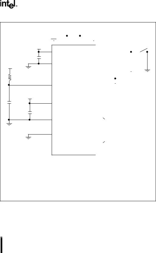
CHAPTER 13 MINIMUM HARDWARE CONSIDERATIONS
The 8XC196Kx, Jx, and CA have several basic requirements for operation within a system. This chapter describes options for providing the basic requirements and discusses other hardware considerations.
13.1 MINIMUM CONNECTIONS
Table 13-1 lists the signals that are required for the device to function and Figure 13-1 shows the connections for a minimum configuration.
|
|
Table 13-1. Minimum Required Signals |
|
Signal |
Type |
Description |
|
Name |
|||
|
|
||
|
|
|
|
ANGND |
GND |
Analog Ground |
|
|
|
ANGND must be connected for A/D converter and port 0 operation. ANGND and |
|
|
|
VSS should be nominally at the same potential. |
|
RESET# |
I/O |
Reset |
|
|
|
A level-sensitive reset input to and open-drain system reset output from the micro- |
|
|
|
controller. Either a falling edge on RESET# or an internal reset turns on a pull-down |
|
|
|
transistor connected to the RESET# pin for 16 state times. In the powerdown and |
|
|
|
idle modes, asserting RESET# causes the chip to reset and return to normal |
|
|
|
operating mode. The microcontroller resets to 2080H. |
|
|
|
|
|
VCC |
PWR |
Digital Supply Voltage |
|
|
|
Connect each VCC pin to the digital supply voltage. |
|
VPP |
PWR |
Programming Voltage |
|
|
|
During programming, the VPP pin is typically at +12.5 V (VPP voltage). Exceeding the |
|
|
|
maximum VPP voltage specification can damage the device. |
|
|
|
VPP also causes the device to exit powerdown mode when it is driven low for at least |
|
|
|
50 ns. Use this method to exit powerdown only when using an external clock source |
|
|
|
because it enables the internal phase clocks, but not the internal oscillator. |
|
|
|
On devices with no internal nonvolatile memory, connect VPP to VCC. |
|
|
|
|
|
VREF |
PWR |
Reference Voltage for the A/D Converter |
|
|
|
This pin also supplies operating voltage to both the analog portion of the A/D |
|
|
|
converter and the logic used to read port 0. |
|
|
|
|
|
VSS |
GND |
Digital Circuit Ground |
|
|
|
Connect each VSS pin to ground through the lowest possible impedance path. |
13-1

8XC196Kx, Jx, CA USER’S MANUAL
|
|
Table 13-1. Minimum Required Signals(Continued) |
|
Signal |
Type |
Description |
|
Name |
|||
|
|
||
|
|
|
|
XTAL1 |
I |
Input Crystal/Resonator or External Clock Input |
|
|
|
Input to the on-chip oscillator and the internal clock generators. The internal clock |
|
|
|
generators provide the peripheral clocks, CPU clock, and CLKOUT signal. When |
|
|
|
using an external clock source instead of the on-chip oscillator, connect the clock |
|
|
|
input to XTAL1. The external clock signal must meet the VIH specification for XTAL1 |
|
|
|
(see datasheet). |
|
|
|
|
|
XTAL2 |
O |
Inverted Output for the Crystal/Resonator |
|
|
|
Output of the on-chip oscillator inverter. Leave XTAL2 floating when the design uses |
|
|
|
a external clock source instead of the on-chip oscillator. |
|
|
|
|
13.1.1 Unused Inputs
For predictable performance, it is important to tie unused inputs to VCC or VSS. Otherwise, they can float to a mid-voltage level and draw excessive current. Unused interrupt inputs may generate spurious interrupts if left unconnected.
13.1.2 I/O Port Pin Connections
Tie unused input-only port inputs to VSS as shown in Figure 13-1. Chapter 6, “I/O Ports,” contains information about initializing and configuring the ports. Table 13-2 lists the sections, with page numbers, that contain the information for each port.
|
Table 13-2. I/O Port Configuration Guide |
Port |
Where to Find Configuration Information |
|
|
Port 0 |
“Standard Input-only Port Considerations” on page 6-3 |
Ports 1 and 2 |
“Bidirectional Port Pin Configurations” on page 6-10 and “Bidirectional Port Considerations” |
|
on page 6-12 |
|
|
Ports 3 and 4 |
“Bidirectional Ports 3 and 4 (Address/Data Bus) Operation” on page 6-16 |
Ports 5 and 6 |
“Bidirectional Port Pin Configurations” on page 6-10 and “Bidirectional Port Considerations” |
|
on page 6-12 |
13-2
MINIMUM HARDWARE CONSIDERATIONS
VCC
0.01 µF
VCC
1 M
(Note 3)
VCC
+
1 µF
+
1 µF
|
|
|
|
|
(Note 1) |
|
|
|
|
|
|
|
|
|
|
|
|
|
|
|
|
|
|
|
||||||||||
|
|
20 pF |
|
|
|
|
20 pF |
|
|
|
|
|
|
|
|
|
|
|
|
|
|
|
|
|
|
|
||||||||
|
|
|
|
|
|
|
|
|
|
|
|
|
|
|
|
|
|
|
|
|
|
|
|
|
|
|
|
|
|
|
|
|
|
|
|
|
|
|
|
|
|
|
|
|
|
|
|
|
|
|
|
|
|
|
|
|
|
|
|
|
|
|
|
|
|
|
|
|
|
|
|
|
|
|
|
|
|
|
|
|
|
|
|
|
|
|
|
|
|
|
|
|
|
|
|
|
|
|
|
|
|
|
|
|
|
|
|
|
|
|
|
|
|
|
|
|
|
|
|
|
|
|
|
|
|
|
|
|
|
|
|
|
|
|
|
|
|
|
|
|
|
|
|
|
|
|
|
|
|
|
|
|
|
|
|
|
|
|
|
|
|
|
|
|
|
|
|
|
|
|
|
|
|
|
|
|
|
|
|
|
|
|
|
|
|
|
|
|
|
|
|
|
|
|
|
|
|
|
|
|
|
|
|
|
|
|
|
|
|
|
|
|
XTAL2 |
|
XTAL1 |
|
|
|
|
|
|
|
|
|
|
|
|
|
|
|
|
|
|
|
||||||||||
|
VCC |
|
|
|
RESET# |
|
|
|
|
|
|
|
|
|
|
|
|
|
|
|
|
|
|
|
||||||||||
|
|
|
|
|
|
|
|
|
|
|
|
|
|
|
|
|
|
|
||||||||||||||||
|
(Note 2) |
|
|
|
|
|
|
|
|
|
|
|
VCC |
|
|
|
|
|
|
|
|
|
|
|
|
|
||||||||
|
|
|
|
|
|
|
|
|
|
|
|
|
|
|
|
|
|
|
|
|
|
|
|
|
|
+ |
|
|
||||||
|
VSS |
|
|
|
|
|
EA# |
|
|
|
|
|
|
|
|
|
|
|
|
|
|
4.7 µF |
||||||||||||
|
|
|
|
|
|
|
|
|
|
|
|
|
|
|
|
|
|
|
|
|
|
|
||||||||||||
|
|
|
|
|
|
|
|
|
|
|
|
|
|
|
|
|
|
|
|
|
|
|
|
|
||||||||||
|
|
|
|
|
|
|
|
|
|
|
|
NMI |
|
|
|
|
|
|
|
|
|
|
|
|
|
|
|
|
|
|
|
|||
|
VPP |
|
|
BUSWIDTH |
|
|
|
|
|
|
|
|
|
|
|
|
|
|
|
|
|
|
|
|||||||||||
|
|
|
|
|
|
|
|
|
|
|
|
|
|
|
|
|
|
|
|
|||||||||||||||
|
|
|
|
|
|
|
|
|
|
|
|
|
|
|
|
|
|
|
|
|
|
|
|
|
|
|
|
|
||||||
|
|
|
|
|
|
|
|
|
|
|
|
|
|
|
|
|
|
|
|
|
|
|
|
|
|
|
|
|
||||||
|
|
|
|
|
|
|
|
|
|
|
|
|
|
|
|
|
|
|
|
|
|
|
|
|
|
|
|
|
||||||
|
|
|
|
|
|
|
|
|
|
|
|
|
|
|
|
|
VCC |
|
|
|
|
|
|
|
|
|
|
|
|
|
||||
|
VREF |
|
|
|
|
READY |
|
|
|
|
|
|
|
|
|
|
|
|
|
|
|
|
|
|
|
|||||||||
|
|
|
|
|
|
|
|
|
|
|
|
|
|
|
|
|
|
|
|
|
|
|
|
|||||||||||
|
|
|
|
|
|
|
|
|
|
|
|
|
|
|
|
|
|
|
|
|
|
|
|
|
|
|
|
|
||||||
|
ANGND |
|
|
|
|
|
BHE# |
|
|
|
|
|
|
|
|
|
|
|
|
|
|
|
|
|
|
|
||||||||
|
|
|
|
|
|
|
|
|
|
|
|
|
|
|
|
|
|
|
|
|
|
|
|
|
||||||||||
|
|
|
|
|
|
RD# |
|
|
|
|
|
|
Port 5 / Bus Control |
|||||||||||||||||||||
|
|
|
|
|
|
|
|
|
|
|
|
|
|
|
|
|
|
|||||||||||||||||
|
|
|
|
|
|
|
|
|
|
|
|
|
||||||||||||||||||||||
|
|
|
|
|
|
|
|
|
|
|
|
WR# |
|
|
|
|
|
|
||||||||||||||||
|
Input-only |
|
|
|
|
|
|
|
|
|
|
|
|
|
(Note 4) |
|||||||||||||||||||
|
|
|
|
|
|
|
|
|
|
|
|
|
|
|
|
|
|
|||||||||||||||||
|
|
|
|
|
|
INST |
|
|
|
|
|
|
|
|
|
|
|
|
|
|
|
|
|
|
|
|||||||||
|
Port Pins |
|
|
|
|
|
|
|
|
|
|
|
|
|
|
|
|
|
|
|
|
|
|
|
|
|||||||||
|
|
|
|
|
|
|
|
|
|
|
|
|
|
|
|
|
|
|
|
|||||||||||||||
|
|
|
|
|
|
|
|
|
|
|
|
|
|
|
|
|
|
|
|
|
|
|
|
|
|
|
|
|
||||||
|
(Note 5) |
|
|
|
|
|
ALE |
|
|
|
|
|
|
|
|
|
|
|
|
|
|
|
|
|
|
|
||||||||
|
|
|
|
|
|
|
|
|
|
|
|
|
|
|
|
|
|
|
|
|
|
|
|
|||||||||||
|
|
|
|
8XC196 Device |
|
|
|
|
|
|
|
|
|
|
|
|
|
|
|
|
|
|
|
|||||||||||
|
|
|
|
|
|
|
|
|
|
|
|
|
|
|
|
|
|
|
|
|
|
|
|
|
|
|
|
|
|
|
|
|
|
|
Notes:
1.See the datasheet for the oscillator frequency range (FOSC) and the crystal manufacturer's datasheet for recommended load capacitors.
2.The number of VCC and VSS pins varies with package type (see datasheet). Be sure to connect each VCC pin to the supply voltage and each VSS pin to ground.
3.Connect the RC network to VPP only if powerdown mode will be used. Otherwise, connect VPP to VCC.
4.No connection is required.
5.Tie all input-only port pins to VSS.
A2643-02
Figure 13-1. Minimum Hardware Connections
13-3