


STANDARD AND PTS INTERRUPTS
When the next timer match occurs, the PTS cycle (Figure 5-17) increments EPA0_TIME by T1 (if TBIT is zero (output = 0)) or T2 – T1 (if TBIT is one (output = 1)). (Note that although the values of the EPA0 output and TBIT are the same in this example, these two values are unrelated. To establish the initial value of the output, set or clear P1_REG.x.)
The PWM toggle mode has the advantage of using only one EPA channel. However, if the waveform edges are close together, the PTS may take too long and miss setting up the next edge. The PWM remap mode uses two EPA channels to eliminate this problem.
5.6.6.2PWM Remap Mode Example
Figure 5-18 shows the PTS control block for PWM remap mode. This example uses two EPA channels and a single timer to generate a PWM waveform in PWM remap mode. EPA0 sets the output, and EPA1 clears it. For each channel, an interrupt is generated every T2 period, but the comparison times for the channels are offset by the on-time, T1 (see Figure 5-15 on page 5-32). Although TBIT is toggled at the end of every PWM remap mode cycle (see Table 5-12 on page 5-31), it plays no role in this mode. To generate a PWM waveform, follow this procedure.
1.Disable the interrupts and the PTS. The DI instruction disables all interrupts; the DPTS instruction disables the PTS.
2.Set up one PTSCB for EPA0 and one for EPA1 as shown in Table 5-14. Note that the two blocks are identical, except that PTSPTR1 points to EPA0_TIME for EPA0 and to EPA1_TIME for EPA1.
3.Configure P1.1 to serve as the EPA1 output. (Because EPA0 is not used as an output, port pin P1.0 can be used for standard I/O.)
—Clear P1_DIR.1 (selects output)
—Set P1_MODE.1 (selects the EPA0 special-function signal)
—Set P1_REG.1 (initializes the output to “1”)
5-37

8XC196Kx, Jx, CA USER’S MANUAL
Table 5-14. PWM Remap Mode PTSCB
PTSCB0 for EPA0 |
PTSCB1 for EPA1 |
|
|
Unused |
Unused |
|
|
Unused |
Unused |
|
|
PTSCONST1 (HI) = T2 (HI) |
PTSCONST1 (HI) = T2 (HI) |
|
|
PTSCONST1 (LO) = T2 (LO) |
PTSCONST1 (LO) = T2 (LO) |
|
|
PTSPTR1 (HI) = 1FH (EPA0_TIME, HI) |
PTSPTR1 (HI) = 1FH (EPA1_TIME, HI) |
|
|
PTSPTR1 (LO) = 62H (EPA0_TIME, LO) |
PTSPTR1 (LO) = 66H (EPA1_TIME, LO) |
|
|
PTSCON = 40H (Mode = 010, TMOD = 0) |
PTSCON = 40H (Mode = 010, TMOD = 0) |
|
|
Unused |
Unused |
|
|
4.Set up EPA0 and EPA1:
—Load EPA0_CON with 68H (timer 1, compare mode, set output pin, re-enable).
—Load EPA1_CON with 158H (timer 1, compare mode, clear output pin, re-enable, remap enabled).
—Load EPA0_TIME with 0000H (selects time 0 as first event time for EPA0).
—Load EPA1_TIME with the value of T1 (selects time T1 as first event time for EPA1).
—Load timer 1 with FFFFH to ensure that the EPA0 event time (t = 0) is matched first.
—Load T1CONTROL with C2H (enables timer 1, selects up-counting at F OSC/4, and enables the divide-by-four prescaler).
5.Enable the EPA0 and EPA1 interrupts and select PTS service for them:
—Set INT_MASK.4 and INT_MASK.3.
—Set PTSSEL.4 and PTSSEL.3
6.Enable the interrupts and the PTS. The EI instruction enables interrupts; the EPTS instruction enables the PTS.
5-38

STANDARD AND PTS INTERRUPTS
PTS PWM Remap Mode Control Block
In PWM remap mode, the PTS uses two EPA channels to generate a pulse-width modulated (PWM) output signal. The control block contains registers that contain the PWM on-time (PTSCONST1), the address pointer (PTSPTR1), and a control register (PTSCON).
|
|
7 |
|
|
|
|
|
|
|
|
|
0 |
||
Unused |
|
0 |
0 |
|
0 |
0 |
|
0 |
|
0 |
0 |
0 |
||
|
|
|
7 |
|
|
|
|
|
|
|
|
|
0 |
|
|
|
|
|
|
|
|
|
|
|
|
|
|
|
|
Unused |
|
0 |
0 |
|
0 |
0 |
|
0 |
|
0 |
0 |
0 |
||
|
|
|
15 |
|
|
|
|
|
|
|
|
|
8 |
|
|
|
|
|
|
|
|
|
|
|
|
|
|
||
PTSCONST1 (HI) |
|
|
|
|
PWM Const 1 Value (high byte) |
|
|
|||||||
|
|
|
7 |
|
|
|
|
|
|
|
|
|
0 |
|
|
|
|
|
|
|
|
|
|
|
|
|
|
||
PTSCONST1 (LO) |
|
|
|
|
PWM Const 1 Value (low byte) |
|
|
|||||||
|
|
|
15 |
|
|
|
|
|
|
|
|
|
8 |
|
|
|
|
|
|
|
|
|
|
|
|
|
|
|
|
PTSPTR1 (HI) |
|
|
|
|
|
Pointer 1 Value (high byte) |
|
|
|
|||||
|
|
|
7 |
|
|
|
|
|
|
|
|
|
0 |
|
|
|
|
|
|
|
|
|
|
|
|
|
|
|
|
PTSPTR1 (LO) |
|
|
|
|
|
Pointer 1 Value (low byte) |
|
|
|
|||||
|
|
|
7 |
|
|
|
|
|
|
|
|
|
0 |
|
|
|
|
|
|
|
|
|
|
|
|
|
|
|
|
PTSCON |
|
|
M2 |
M1 |
|
M0 |
— |
|
— |
|
— |
TMOD |
TBIT |
|
|
|
|
7 |
|
|
|
|
|
|
|
|
|
0 |
|
|
|
|
|
|
|
|
|
|
|
|
|
|
|
|
Unused |
|
0 |
0 |
|
0 |
0 |
|
0 |
|
0 |
0 |
0 |
||
|
|
|
|
|
|
|
|
|
|
|
|
|
|
|
Register |
|
Location |
|
|
|
|
Function |
|
|
|
||||
|
|
|
|
|
|
|
|
|
|
|
|
|||
PTSCONST1 |
|
PTSCB + 4 |
PWM Const 1 Value |
|
|
|
|
|
|
|
|
|||
|
|
|
|
Write the desired PWM on-time to these bits. |
|
|
|
|||||||
|
|
|
|
|
|
|
|
|
|
|
|
|||
PTSPTR1 |
|
PTSCB + 2 |
Pointer 1 Value |
|
|
|
|
|
|
|
|
|||
|
|
|
|
These bits point to a memory location, usually EPAx_TIME. |
|
|||||||||
|
|
|
|
|
|
|
|
|
|
|
|
|
|
|
Figure 5-18. PTS Control Block – PWM Remap Mode
5-39

8XC196Kx, Jx, CA USER’S MANUAL
PTS PWM Remap Mode Control Block (Continued)
Register |
Location |
|
|
|
|
|
Function |
|
|
|
|
|
|
|
|
||
PTSCON |
PTSCB + 1 |
PTS Control Bits |
|
|
|
|||
|
|
|
|
|
|
|
||
|
|
|
M2:0 |
PTS Mode |
|
|
||
|
|
|
|
These bits specify the PTS mode: |
||||
|
|
|
|
M2 |
M1 |
M0 |
|
|
|
|
|
|
0 |
|
1 |
0 |
PWM |
|
|
|
|
|
||||
|
|
|
TMOD |
Remap Mode Select |
||||
|
|
|
|
0 |
= PWM remap mode |
|||
|
|
|
|
|
||||
|
|
|
TBIT |
Toggle Bit Initial Value |
||||
|
|
|
|
Determines the initial value of TBIT. |
||||
|
|
|
|
1 |
= selects initial value as one |
|||
|
|
|
|
0 |
= selects initial value as zero |
|||
|
|
|
|
The TBIT value determines whether PTSCONST1 or |
||||
|
|
|
|
PTSCONST2 is added to the PTSPTR1 value: |
||||
|
|
|
|
1 |
= PTSCONST2 is added to PTSPTR1 |
|||
|
|
|
|
0 |
= PTSCONST1 is added to PTSPTR1 |
|||
|
|
|
|
Reading this bit returns the current value of TBIT, which is |
||||
|
|
|
|
toggled by hardware at the end of each PWM remap cycle. |
||||
|
|
|
|
In PWM remap mode, the TBIT value is not used; PTSCONST1 |
||||
|
|
|
|
is always added to the PTSPTR1 value. However, the unused |
||||
|
|
|
|
TBIT still toggles at the end of each PWM remap cycle. |
||||
|
|
|
|
|
|
|
|
|
Figure 5-18. PTS Control Block – PWM Remap Mode (Continued)
Figure 5-19 shows the EPA and PTS operations for this example. The first timer match occurs at t = 0 for EPA0, which sets the output and generates an interrupt.
PWM Remap Cycle 1. The PTS adds T2 to EPA0_TIME and toggles the TBIT.
The output remains set until the second timer match occurs at T1 for EPA1, which clears the output and generates an interrupt.
PWM Remap Cycle 2. The PTS adds T2 to EPA1_TIME and toggles the TBIT.
Alternating EPA0 and EPA1 interrupts continue, with EPA0 setting the output and EPA1 clearing it.
5-40
STANDARD AND PTS INTERRUPTS
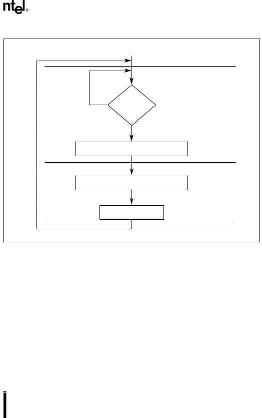
Start
EPA
No |
Timer |
|
Match |
|
? |
|
Yes |
If EPA0, set the output
If EPA1, clear the output
PTSPTSCycle
If EPA0: EPA0_TIME = EPA0_TIME + T2
If EPA1: EPA1_TIME = EPA1_TIME + T2
Toggle TBIT (TBIT is not used)
A2553-01
Figure 5-19. EPA and PTS Operations for the PWM Remap Mode Example
You can change the duty cycle by changing the time that the output is high and keeping the period constant. After a timer match occurs for EPA1 (when the output falls), schedule the next EPA1 match for T2 + DT, where DT is the time to be added to the on-time. Thereafter, schedule the next EPA1 match for T2. You can do this by replacing one EPA1 PTS interrupt with a normal interrupt (clear PTSSEL.3). Have the interrupt service routine add T2 + DT to EPA1_TIME and set PTSSEL.3 to re-enable PTS service for EPA1. This adjustment changes the duty cycle without affecting the period.
By using two EPA channels in the PWM remap mode, you can generate duty cycles closer to 0% and 100% than is possible with PWM toggle mode. For further information about generating PWM waveforms with the EPA, consult “Operating in Compare Mode” on page 10-13.
5-41

6
I/O Ports