


8XC196Kx, Jx, CA USER’S MANUAL
16.10 SERIAL PORT PROGRAMMING MODE
The serial port programming mode enables the serial I/O (SIO) port to write data to the OTPROM through the TXD (P2.0) pin and read it through the RXD (P2.1) pin. In this mode, the device executes a program from its internal test ROM. This program is a modified version of the reduced instruction set monitor (RISM) that exists on all 8X9X evaluation boards. The simple hardware setup of this mode makes it useful for in-module testing, programming, and in-line diagnostics. Special software, called IBSP196, simplifies communication between the device and a smart terminal. This software is available free of charge through the Intel BBS. (See “Bulletin Board System (BBS)” on page 1-9.)
NOTE
Serial port programming mode has no provision for security-key verification. If a security key has been programmed, an attempt to enter serial port programming mode causes the device to enter an endless loop.
Entering serial port programming mode with VPP at +12.5 volts allows you to modify code in OTPROM or to program small segments of OTPROM to customize code for a particular module. (Programming more than 2 Kbytes of OTPROM is not recommended in this mode because of its relatively long programming time.)
Entering serial port programming mode with VPP at +5.0 volts enables you to perform these functions:
•download a module-testing program into internal RAM and execute it without altering nonvolatile memory or using dedicated OTPROM software space
•run a segment of code in OTPROM and monitor its performance during execution
•examine the code programmed into the OTPROM
•examine the contents of any register
•manipulate RAM, SFRs, or pin states
16.10.1 Serial Port Programming Circuit and Memory Map
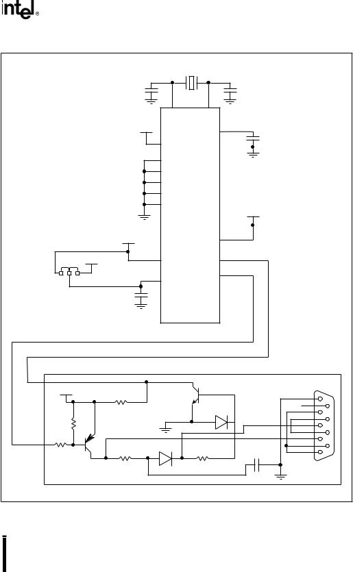
Figure 16-14 shows the recommended circuit for serial port programming. In this mode, data is transmitted and received through the TXD (P2.0) and RXD (P2.1) pins. Connect these pins to any smart terminal capable of communicating with the RISM. Any host that requires an RS-232C interface (such as a PC) must be connected through an RS-232C driver/receiver such as the one shown within the dashed line in Figure 16-14. XTAL1 and XTAL2 can be connected to a crystal with a frequency between 3.5 MHz and 16 MHz. The frequency must correspond to the value in the SP_BAUD register (see “Changing Serial Port Programming Defaults” on page 16-34).
16-32
PROGRAMMING THE NONVOLATILE MEMORY
|
30 pF |
|
|
30 pF |
|
|
|
XTAL1 |
|
XTAL2 |
|
|
VCC |
|
|
RESET# |
|
|
|
VREF |
|
10 µF |
|
|
|
|
NMI |
|
|
|
|
P0.7/PMODE.3 |
|
||
|
|
P0.6/PMODE.2 |
|
||
|
|
P0.5/PMODE.1 |
|
||
|
|
P0.4/PMODE.0 |
|
||
|
|
ANGND |
|
VCC |
|
|
|
|
|
|
|
|
|
READY/P5.6 |
|
||
|
VPP |
BUSWIDTH/5.7 |
|
||
|
VCC |
EA# |
P2.1/RXD |
|
|
A |
B C |
VPP |
|
P2.0/TXD |
|
|
|
|
|||
|
|
|
|
|
|
|
0.01 µF |
|
|
|
|
|
|
87C196 Device |
|
||
RXD |
|
|
|
|
|
VCC |
|
|
|
5 |
|
|
|
2N2222A |
|
||
|
|
|
9 |
||
|
1.8kΩ |
|
|
1N914 |
4 |
|
|
|
|
RXD |
8 |
1.8kΩ |
|
|
|
3 |
|
|
2N2907 |
|
|
TXD |
7 |
TXD |
|
|
|
2 |
|
|
|
|
|
6 |
|
|
|
|
|
|
|
1.8kΩ |
|
|
|
|
1 |
|
|
|
|
|
|
|
1.8kΩ |
1N914 |
|
1.8kΩ |
|
|
|
|
10µF |
|
|
|
|
|
|
|
|
|
|
|
|
|
A0298-04 |
Figure 16-14. Serial Port Programming Mode Circuit
16-33

8XC196Kx, Jx, CA USER’S MANUAL
Because the RISM begins at location 2000H in serial port programming mode, the OTPROM locations are automatically remapped as shown in Table 16-12. For example, to access OTPROM location 2000H in serial port programming mode, you must address it as A000H.
Table 16-12. Serial Port Programming Mode Memory Map
|
|
Address Range (Hex) |
||
|
|
|
|
|
Description |
Device |
Normal |
Serial Port |
|
|
|
Operation |
Programming Mode |
|
|
|
|
|
|
|
87C196JV |
2000–DFFF |
A000–FFFF, 8000–DFFF† |
|
|
87C196CA, JT, KT |
2000–9FFF |
A000–FFFF, 8000–9FFF†† |
|
Internal OTPROM |
87C196KS |
2000–7FFF |
A000–FFFF |
|
|
|
|
|
|
|
87C196JR, KR |
2000–5FFF |
A000–DFFF |
|
|
|
|
|
|
|
87C196JQ, KQ |
2000–4FFF |
A000–CFFF |
|
|
|
|
|
|
External memory |
87C196CA, JT, KT, JV |
— |
4000–7FFF |
|
|
|
|
||
87C196JQ, KQ, JR, KR, KS |
— |
4000–9FFF |
||
|
||||
|
|
|
|
|
Do not address |
All |
— |
2400–3FFF |
|
|
|
|
|
|
Test ROM and RISM |
All |
— |
2000–23FF |
|
|
|
|
|
|
† For the 87C196JV, the lower 24 Kbytes of internal OTPROM (2000–7FFFH) are remapped to A000– FFFFH. The upper 24 Kbytes must be addressed as 8000–DFFFH. A bank switching mechanism differentiates between the two address ranges. To program the upper 24 Kbytes of the internal OTPROM, execute this instruction: orb tmr, #80h.
†† For the 87C196CA, JT, and KT, the lower 24 Kbytes of internal OTPROM (2000–7FFFH) are remapped to A000–FFFFH. The upper 8 Kbytes must be addressed as 8000–9FFFH.
16.10.2 Changing Serial Port Programming Defaults
Several locations in test ROM are used to control operating parameters. The test ROM routine establishes the default values shown in Table 16-13. To change the default values, write the desired values to the test ROM addresses shown in the table. (Refer to the SP_BAUD, SP_CON, and SP_PPW register descriptions in Appendix C.) After you write the new values to the test ROM locations, the RISM writes the programmed values into the associated registers.
The default programming pulse width is longer than required. To avoid unnecessarily long programming times, change the default value before beginning to program the device. For a 100-µs pulse width, use the following formula to determine the required PPW_VALUE and write that value to the test ROM location listed in Table 16-13.
PPW_VALUE = ( 0.6944 × Fosc) – 1
16-34

PROGRAMMING THE NONVOLATILE MEMORY
Table 16-13. Serial Port Programming Default Values and Locations
|
|
Test ROM Address |
Test ROM |
|
Parameter |
RISM Default |
(CA, JQ, JR, |
Address |
SFR |
|
|
JT, JV, KQ, KR) |
(KS, KT) |
|
|
|
|
|
|
Mode |
09H; mode 1, receiver enabled |
2213H |
2215H |
SP_CON |
|
|
|
|
|
Baud rate |
8067H; 9600 baud at 16 MHz |
2214H |
2216H |
SP_BAUD |
|
|
|
|
|
Pulse width |
80FFH; 2.30ms per pulse at 16 MHz |
2216–2217H |
221C–221DH |
SP_PPW |
|
|
|
|
|
16.10.3 Executing Programs from Internal RAM
For those wanting to execute user programs from internal RAM while in serial port programming mode, the RISM allows you to initialize the user program counter (PC), window selection register (WSR), and processor status word (PSW). Table 16-14 lists the registers, the default assumed by the RISM, and the test ROM address to which you may write new values.
Before attempting to execute a program from internal RAM or OTPROM, write the beginning address of the program to the PC at the test ROM address shown in Table 16-14. You need not change the WSR and PSW unless other flags need to be set for the program you are executing. After writing the PC value, issue the GO command, which automatically initializes the PC and begins code execution. When the RISM interrupts or halts the program, it writes the user PC, WSR (which includes INT_MASK1), and PSW (which includes INT_MASK) to the test ROM locations.
Internal RAM locations 4EH– 63H are used as registers for serial port programming mode. Programs executing from internal RAM should not alter these locations.
Table 16-14. User Program Register Values and Test ROM Locations
User Program Register |
RISM Default |
Test ROM Address |
|
|
|
PC |
2080H |
5EH |
|
|
|
WSR |
1000H |
60H |
|
|
|
PSW |
0200H |
62H |
|
|
|
16.10.4 Reduced Instruction Set Monitor (RISM)
When you enter serial port programming mode, the device begins executing its RISM program. You communicate with the device by sending RISM commands from any smart terminal across the TXD and RXD pins at a fixed baud rate.
16-35