

Constr_materials
.pdfadjacent grains impinge on one another as the solidification process approaches completion. As indicated in Figure 2.7, the crystallographic orientation varies from grain to grain. Also, there exists some atomic mismatch within the region where two grains meet; this area is called a grain boundary.
Figure 2.6 Scheme showing solidification of a polycrystalline material.
Upon completion of solidification, grains of irregular shapes have formed
Figure 2.7 The grain structure and fracture as they appear under the microscope; dark lines are the grain boundaries
2.6.ANISOTROPY
The physical properties of single crystals of some substances depend on the crystallographic direction in which measurements are taken. For example, the elastic modulus, the electrical conductivity, and the index of refraction may have different values in the [100] and [111] directions. This directionality of properties is termed anisotropy and it is associated with the variance of atomic or ionic spacing with crystallographic direction. Substances in which measured properties are independent of the direction of measurement are isotropic. The extent and magnitude of anisotropic effects in crystalline materials are functions of the symmetry of the crystal structure;
21
Created with novaPDF Printer (www.novaPDF.com). Please register to remove this message.
the degree of anisotropy increases with decreasing structural symmetry – triclinic structures are normally highly anisotropic. The modulus of elasticity values at [100], [110], and [111] orientations for several materials are presented in Table 2.3.
For many polycrystalline materials, the crystallographic orientations of the individual grains are totally random. Under these circumstances, even though each grain may be anisotropic, a specimen composed of the grain aggregate behaves isotropically. Also, the magnitude of a measured property represents some average of the directional values. Sometimes the grains in polycrystalline materials have a preferential crystallographic orientation, in this case the material is said to have a “texture”.
Table 2.3 Modulus of Elasticity Values for Several Metals at Various Crystallographic Orientations
Metal |
|
Modulus of Elasticity (GPa) |
|
||
[100] |
|
[110] |
|
[111] |
|
|
|
|
|||
Aluminum |
63.7 |
|
72.6 |
|
76.1 |
Copper |
66.7 |
|
130.3 |
|
191.1 |
Iron |
125.0 |
|
210.5 |
|
272.7 |
Tungsten |
384.6 |
|
384.6 |
|
384.6 |
2.7.NONCRYSTALLINE SOLIDS
It has been mentioned that noncrystalline solids lack a systematic and regular arrangement of atoms over relatively large atomic distances. Sometimes such materials are also called amorphous (meaning literal – without form), or supercooled liquids, inasmuch as their atomic structure resembles that of a liquid.
An amorphous condition may be illustrated by comparison of the crystalline and noncrystalline structures of the ceramic compound silicon dioxide (SiO2), which may exist in both states. Figures 2.8, a and 2.8, b present two-dimensional schematic diagrams for both structures of SiO2, even though each silicon ion bonds to three oxygen ions for both states. Beyond this, the structure is much more disordered and irregular for the noncrystalline structure.
Whether a crystalline or amorphous solid form depends on the ease with which a random atomic structure in the liquid can transform to an ordered state during solidification. Amorphous materials, therefore, are characterized by atomic or molecular structures that are relatively complex and become ordered only with some difficulty. Furthermore, rapidly cooling through the freezing temperature favors the formation of a noncrystalline solid, since little time is allowed for the ordering process.
22
Created with novaPDF Printer (www.novaPDF.com). Please register to remove this message.

Silicon atom
Oxygen atom
a
b
Figure 2.8 Two-dimensional schemes of the structure:
a – of crystalline silicon dioxide; b – of noncrystalline silicon dioxide
Metals normally form crystalline solids; but some ceramic materials are crystalline, whereas others, the inorganic glasses, are amorphous. Polymers may be completely crystalline, entirely noncrystalline, or a mixture of the two.
Questions and problems
1.Why is a unit cell chosen for the analysis of crystal structures?
2.What does the unit cell define?
3.What kind of unit cell do we usually use, drawing a scheme of crystal structure?
4.How can be solids classified?
5.What do the properties of crystalline solids depend on?
6.Describe BCC, FCC, and HCP crystal structures.
7.What is the result when the repeated arrangement is perfect?
8.How should crystal structures be divided?
9.Which cubic system has the best symmetry?
10.What are the parts of the conventional hexagonal unit cell?
11.Using data of Table 2.3 explain the notion “anisotropy”.
12.What are linear (a, b, c) and angle (α, β, γ) parameters for seven crystal system? Use the Table 2.2.
13.Why polycrystalline materials are not anisotropic?
23
Created with novaPDF Printer (www.novaPDF.com). Please register to remove this message.
3. IMPERFECTIONS IN SOLIDS
In previous chapter it has been assumed that perfect order exists throughout crystalline materials on an atomic scale. However, such an idealized solid does not exist; all contain large numbers of various defects or imperfections. As a matter of fact, many of the properties of materials are profoundly sensitive to deviations from crystalline perfection; the influence is not always adverse, and often specific characteristics are deliberately fashioned by the introduction of controlled amounts or numbers of particular defects, as detailed in succeeding chapters.
By “crystalline defect” is meant a lattice irregularity having one or more of its dimensions on the order of an atomic diameter. Classification of crystalline imperfections is frequently made according to geometry or dimensionality of the defect. Several different imperfections are discussed in this chapter, including point defects (those associated with one or two atomic positions), linear (or one-dimensional) defects, as well as interfacial defects, or boundaries, which are two-dimensional. Impurities in solids are also discussed, since impurity atoms may exist as point defects. Finally, techniques for the microscopic examination of defects and the structure of materials are briefly described.
3.1.POINT DEFECTS
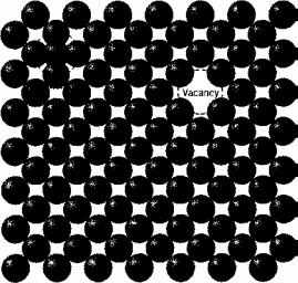
Vacancies and self-interstitials
The simplest of the point defects is a vacancy, or vacant lattice site, one normally occupied from which an atom is missing (Figure 3.1). All
|
crystalline |
solids contain |
vacancies |
|
|
and, in fact, it is not possible to create |
|||
|
such a material that is free of these |
|||
|
defects. The necessity of the existence of |
|||
|
vacancies is explained using principles |
|||
|
of thermodynamics; in essence, the |
|||
|
presence of vacancies increases the |
|||
|
entropy (i. e., the randomness) of the |
|||
|
crystal. |
|
|
|
|
A self-interstitial is an atom from |
|||
|
the crystal that is crowded into an |
|||
|
interstitial site, a small void space that |
|||
Figure 3.1 Two-dimensional |
under ordinary circumstances is not |
|||
occupied. This kind of defect is also |
||||
representations of a vacancy and |
||||
represented |
in Figure 3.1. In |
metals, a |
||
a self-interstitial |
||||
self-interstitial introduces relatively large
24
Created with novaPDF Printer (www.novaPDF.com). Please register to remove this message.
distortions in the surrounding lattice because the atom is substantially larger than the interstitial position in which it is situated. Consequently, the formation of this defect is not highly probable, and it exists in very small concentrations, which are significantly lower than for vacancies.
Impurities in solids
A pure metal consisting of only one type of atom just isn't possible; impurity or foreign atoms will always be present, and some will exist as crystalline point defects. In fact, even with relatively sophisticated techniques, it is difficult to refine metals to purity in excess of 99.9999 %. At this level, on the order of 1022 to 1023 impurity atoms will be present in one cubic meter of material. Most familiar metals are not highly pure; rather, they are alloys, in which impurity atoms have been added intentionally to impart specific characteristics to the material. Ordinarily alloying is used in metals to improve mechanical strength and corrosion resistance. For example, sterling silver is a 92.5 % silver–7.5 % copper alloy. In normal ambient environments, pure silver is highly corrosion resistant, but also very soft. Alloying with copper enhances the mechanical strength significantly, without depreciating the corrosion resistance appreciably.
The addition of impurity atoms to a metal will result in the formation of a solid solution and/or a new second phase, depending on the kinds of impurity, their concentrations, and the temperature of the alloy. The present discussion is concerned with the notion of a solid solution.
Several terms relating to impurities and solid solutions deserve mention. With regard to alloys, solute and solvent are terms that are commonly employed. “Solvent” represents the element or compound that is present in the greatest amount; on occasion, solvent atoms are also called host atoms. “Solute” is used to denote an element or compound present in a minor concentration.
A solid solution forms when, as the solute atoms are added to the host material, the crystal structure is maintained, and no new structures are formed. Perhaps it is useful to draw an analogy with a liquid solution. If two liquids, soluble in each other (such as water and alcohol) are combined, a liquid solution is produced as the molecules intermix, and its composition is homogeneous throughout. A solid solution is also compositionally homogeneous; the impurity atoms are randomly and uniformly dispersed within the solid.
Impurity point defects are found in solid solutions, of which there are two types: substitutional and interstitial. For substitutional, solute or impurity atoms replace or substitute for the host atoms (Figure 3.2). There are several
25
Created with novaPDF Printer (www.novaPDF.com). Please register to remove this message.

features of the solute and solvent atoms that determine the degree to which the former dissolves in the latter; these are as follows:
1.Atomic size factor. Appreciable quantities of a solute may be accommodated in this type of solid solution only when the difference in atomic radii between the two atom types is less than about ±15 %. Otherwise the solute atoms will create substantial lattice distortions and a new phase will form.
2.Crystal structure. For appreciable solid solubility the crystal structures for metals of both atom types must be the same.
3.Electronegativity. The more electropositive one element and the more electronegative the other, the greater is the likelihood that they will form an intermetallic compound instead of a substitutional solid solution.
4.Valences. Other factors being equal, a metal will have more of a tendency to dissolve another metal of higher valency than one of a lower valency.
An example of a substitutional solid solution is found for copper and nickel. These two elements are completely soluble in one another at all proportions. With regard to the aforementioned rules that govern degree of solubility, the atomic radii for copper and nickel are 0.128 and 0.125 nm, respectively, both have the FCC crystal structure, and their electronegativities are 1.9 and 1.8; finally, the most common valences are +1 for copper (although it sometimes can be +2) and +2 for nickel.
Figure 3.2 Two-dimensional representations of substitutional and interstitial impurity atoms
For interstitial solid solutions, impurity atoms fill the voids or interstices among the host atoms (Figure 3.2). For metallic materials that have relatively high atomic packing factors, these interstitial positions are relatively small. Consequently, the atomic diameter of an interstitial impurity must be substantially
26
Created with novaPDF Printer (www.novaPDF.com). Please register to remove this message.

smaller than that of the host atoms. Normally, the maximum allowable concentration of interstitial impurity atoms is low (less than 10 %). Even very small impurity atoms are ordinarily larger than the interstitial sites, and as a consequence they introduce some lattice strains on the adjacent host atoms.
Carbon forms an interstitial solid solution when 'added to iron; the maximum concentration of carbon is about 2 %. The atomic radius of the carbon atom is much less than that for iron: 0.071 nm versus 0.124 nm. Solid solutions are also possible for ceramic materials.
3.2.DISLOCATIONS – LINEAR DEFECTS
A dislocation is a linear or one-dimensional defect around which some of the atoms are misaligned. One type of dislocation is represented in Figure 3.3: an extra portion of a plane of atoms, or half-plane, the edge of which terminates within the crystal. This is termed an edge dislocation; it is a linear defect that centers around the line that is defined along the end of the extra half-plane of atoms. This is sometimes termed the dislocation line, which, for the edge dislocation in Figure 3.3, is perpendicular to the plane of the page. Within the region around the dislocation line there is some localized lattice distortion. The atoms above the dislocation line in Figure 3.3 are squeezed together, and those below are pulled apart; this is reflected in the slight curvature for the vertical planes of atoms as they bend around this extra half-plane. The magnitude of this distortion decreases with distance
away from the dislocation line; at positions far removed, the crystal lattice is virtually perfect. Sometimes the edge dislocation in Figure 3.3 is represented by the symbol ┴, which also indicates the position of the dislocation line. An edge dislocation may also be formed by an extra half-plane of atoms that is included in the bottom portion of the crystal; its designation is a ┬.
Another type of dislocation, called a screw dislocation, exists, which may be thought of as being formed by a shear stress that is
applied to produce the distortion shown in Figure 3.4: the upper front region of the crystal is shifted one atomic distance to the right relative to the bottom portion. The atomic distortion associated with a screw dislocation is also linear and along a dislocation line (the line goes through point A perpendicular to the
27
Created with novaPDF Printer (www.novaPDF.com). Please register to remove this message.
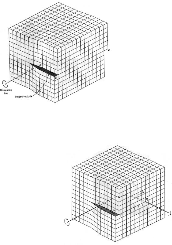
a screw, they are parallel (Fig. 3.4); they are neither perpendicular nor parallel for a mixed dislocation. Also, even though a dislocation changes direction and nature within a crystal (e. g., from edge to mixed to screw), the Burgers vector will be the same at all points along its line. For example, all positions of the curved dislocation in Figure 3.5 will have the Burgers vector shown. For metallic materials, the Burgers vector for a dislocation will point in a closepacked crystallographic direction and will be of magnitude equal to the interatomic spacing.
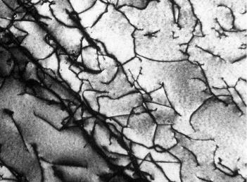
Dislocations can be observed in crystalline materials using electronmicroscopic techniques. In Figure 3.6, a high-magnification transmission electron micrograph, the dark lines are the dislocations.
Figure 3.6 A transmission electron micrograph of a titanium alloy in which the dark lines are dislocations
Virtually all crystalline materials contain some dislocations that were introduced during solidification, during plastic deformation, and as a consequence of thermal stresses that result from rapid cooling. Dislocations are involved in the plastic deformation of crystalline materials.
3.3.INTERFACIAL DEFECTS
Interfacial defects are boundaries that have two dimensions and normally separate regions of the materials that have different crystal structures and/or crystallographic orientations. These imperfections include external surfaces, grain boundaries, twin boundaries, stacking faults, and phase boundaries.
One of the most obvious boundaries is the external surface, along which the crystal structure terminates. Surface atoms are not bonded to the maximum number of nearest neighbors, and are therefore in a higher energy state than the atoms at interior positions. The bonds of these surface atoms that are not
29
Created with novaPDF Printer (www.novaPDF.com). Please register to remove this message.

satisfied give rise to a surface energy, expressed in units of energy per unit area (J/m2 or erg/cm2). To reduce this energy, materials tend to minimize, if at all possible, the total surface area. For example, liquids assume a shape having a minimum area – the droplets become spherical. Of course, this is not possible with solids, which are mechanically rigid.
Another interfacial defect is the grain boundary separating two small grains or crystals having different crystallographic orientations in polycrystalline materials. A grain boundary is represented schematically from an atomic perspective in Figure 3.7. Within the boundary region, which is probably just several atom distances wide, there is some atomic mismatch in a transition from the crystalline orientation of one grain to that of an adjacent one. Various degrees of crystallographic misalignment between adjacent grains are possible (Fig. 3.7). When this orientation mismatch is slight, on the order of a few degrees, then the term small-angle grain boundary is used. These boundaries can be described in terms of dislocation arrays. One simple small-angle grain boundary is formed when edge dislocations are aligned in the manner of Figure 3.8. This type is called a tilt boundary. When the angle of misorientation is parallel to the boundary, a twist boundary results, which can be described by an array of screw dislocations.
The atoms are bonded less regularly along a grain boundary (e. g., bond angles are longer), and consequently, there is an interfacial or grain boundary energy similar to the surface energy described above. The magnitude of this energy is a function of the degree of misorientation, being larger for high-angle boundaries. Grain boundaries are more chemically reactive than the grains themselves as a consequence of this
boundary energy. Furthermore, impurity atoms often preferentially segregate along these boundaries because of their higher energy state. The total interfacial energy is lower in large or coarse-grained materials than in finegrained ones, since there is less total boundary area in the former. Grains grow at elevated temperatures to reduce the total boundary energy.
30
Created with novaPDF Printer (www.novaPDF.com). Please register to remove this message.