

Broadband Packet Switching Technologies
.pdfBroadband Packet Switching Technologies: A Practical Guide to ATM Switches and IP Routers
H. Jonathan Chao, Cheuk H. Lam, Eiji Oki
Copyright 2001 John Wiley & Sons, Inc. ISBNs: 0-471-00454-5 ŽHardback.; 0-471-22440-5 ŽElectronic.
CHAPTER 11
OPTICAL PACKET SWITCHES
Introduction of optical fibers to communication networks has caused a tremendous increase in the speed of data transmitted. The virtually unlimited bandwidth of optical fibers comes from the carrier frequency of nearly 200 THz w1x. Optical networking technology, such as add-drop multiplexers w2, 3x, reconfigurable photonic switches w4x, and wavelength division-multiplexing ŽWDM., has progressed well and facilitated optical networking w5, 6x. Especially, recent advances in dense wavelength multiplexing division ŽDWDM. technology have provided tremendous bandwidth in optical fiber communications w7x. However, the capability of switching and routing packets at this high bandwidth Že.g., 1 Tbitrs. has lagged far behind the transmission capability. Building a large-capacity packet switching system using only electronic technology may lead to a system bottleneck in interconnecting many electronic devices or modules, mainly caused by the enormous number of interconnection wires and the electromagnetic interference they would generate. With the advancement of optical devices technology, several packet switch architectures based on WDM technology have been proposed for large-capacity packet switches. Although today’s optical packet switching technology is still very primitive and cannot compete with electronic switching technology, optical packet switches have great potential to scale up their switching capacity as the technology of some key optical devices becomes mature.
A photonic packet switch requires optical devices such as lasers, filters, couplers, memories, multiplexers, and demultiplexers. At the present time, some of these devices are either too power-consuming or too slow in switching to compete with electronic devices. However, it is possible to design
279
280 OPTICAL PACKET SWITCHES
high-capacity switches by the use of both electronic and optical technologies. In such switches, data transfer can be achieved through optical media, and complicated functions such as contention resolution and routing control can be performed electronically. These switches are called hybrid switches. Hybrid switches that only convert packet cell headers into electronics for processing and controlling and leave the entire cell to be handled in the optical domain are called optically transparent.
The ongoing research in photonic ATM switches is to develop faster and larger optical switches and new techniques that can be used to enhance the existing optical switch architectures. There are many issues to be considered when designing an optical packet switch, such as the characteristics of the optical devices employed, scalability of the switch, power budget of the system, synchronization between electrical and incoming optical signals, performance of the switch under various traffic patterns, and so on. In addition, some of the techniques developed for optical ATM switches might be applied to large-scale ATM switches where small electronic ATM modules are interconnected by an optical interconnection network.
The techniques of space-division multiplexing ŽSDM., time-division multiplexing ŽTDM., and WDM have been used in designing optical switches. SDM requires a large number of binary switching elements. From the switch size and cost point of view, it is not an ideal approach for photonic switching. TDM is a classical technique used in communications w8x. When it is applied to optical switching, complicated temporal compression and temporal expansion circuits are required. The throughput of such a switch is limited by the speed of the demultiplexer, which in practice is controlled by electronics for the time being.
WDM is made possible by the range of wavelengths on an optical fiber. It splits the optical bandwidth of a link into fixed, nonoverlapping spectral bands. Each band has a wavelength channel that can be used for a specific bit rate and transmission technique, independent of the choices for other channels.
In this chapter, we review several approaches to building a large-capacity packet switch and discuss their advantages and disadvantages. These switch architectures are classified into all-optical packet switches Ždescribed in Section 11.1. and optoelectronic packet switches Ždescribed in Section 11.2., depending on whether the contended packets are stored in the optical or in the electrical domain. Two optical packet switches will be described in detail in Sections 11.3 Žusing optical memory. and 11.4 Žusing optics for interconnection only. to better understand switching operations and implementation complexity. In all the architectures presented here, switch control is achieved electronically, since for the time being it is complicated to realize logical operations optically. The capacity of electronic control units and the tuning speed of optical devices are the main performance-limiting factors in these architectures.
ALL-OPTICAL PACKET SWITCHES |
281 |
11.1ALL-OPTICAL PACKET SWITCHES
In optical packet switches, logical control and contention resolution are handled by an electronic controller, and packets are carried and stored in optical memories. There are two kinds of optical memory used in all-optical packet switches: one is the traveling type based on fiber delay lines, and the other is the fiber-loop type where packets carried at different wavelengths coexist in the fiber loop.
11.1.1The Staggering Switch
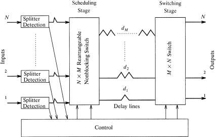
The staggering switch w9x is one of the optically transparent switches. The major components of the switch are splitter detectors, rearrangeable nonblocking switches, and a control unit. The switch architecture is based on two stages: the scheduling stage and the switching stage, as shown in Figure 11.1. These two stages can be considered as rearrangeably nonblocking networks. The scheduling stage and the switching stage are of size N M and M N, respectively, where M is less than N. These two stages are connected by a set of optical delay lines having unequal delay. The idea behind this architecture is to arrange incoming cells in the scheduling stage in such a way that there will be no output port collision in the switching stage. This is achieved by holding the cells that cause output port collision on the delay lines. The delay on the delay line di is equal to i cell slots. The arrangement of incoming cells
Fig. 11.1 Block diagram of the staggering switch. Ž 1993 IEEE..
282 OPTICAL PACKET SWITCHES
is accomplished electronically by the control unit according to the output port requests of incoming cells.
When a cell arrives at the switch, its header information is converted into an electrical signal and sent to the control unit by the corresponding splitter detector. After evaluating the current destination requests considering the previous requests, the control unit sends the information related to the current schedule to the scheduling stage. The cell is routed through the scheduling stage with respect to the information sent by the control unit. Due to the statistical properties of the incoming cells, it is possible to lose some cells in the scheduling stage. After waiting for a certain period of time on the assigned delay line, the cell reaches the switching stage. No contention occurs in the switching stage, on account of the precautions taken by the control unit, and the cell reaches the requested output port. In this architecture, cells arriving at the same input port may arrive at output ports in the reverse order, since they are assigned to different delay lines. Ordered delivery of cells at the output ports can be achieved by some additional operations in the control unit.
The main bottleneck in this switch architecture is the control unit. The proposed collision resolution algorithm is too complicated to handle large switch size or high input line rate. Some input buffers may be necessary in order to keep newly arriving cells while the control unit makes its arrangements.
11.1.2ATMOS
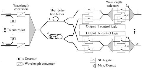
Chiaroni et al. proposed a 16 16 photonic ATM switching architecture w10x for bit rates up to 10 Gbitrs. Basically, this switch consists of three main blocks: the wavelength encoding block, the buffering and time switching block, and the wavelength selection block, as shown in Figure 11.2. In the wavelength encoding block, there are N wavelength converters, one per input. Each input is assigned a fixed wavelength by its wavelength converter. When a cell arrives, a small fraction of the optical signal power is tapped by a coupler and converted to an electronic signal. A controller processes these converted data and extracts the routing information for the cell. The arriving cells with different wavelengths are wavelength-division multiplexed in the buffering and switching block by a multiplexer. The buffering-and-time- switching block contains K fiber delay lines to store the payloads of the incoming cells. There is also a space switch, which is made of semiconductor optical amplifier ŽSOA. gates. These gates are used to select the cells from the fiber delay lines and route them to the requested output ports. The wavelength selection block consists of multiplexerrdemultiplexer and SOA gates in order to select a specific wavelength destined to an output port in a cell time slot. This switch can perform the multicast function by using a broadcast-and-select approach.
ALL-OPTICAL PACKET SWITCHES |
283 |
Fig. 11.2 Architecture of the ATMOS switch.
The cell contention problem is solved by the fiber delay lines. However, this approach cannot provide for sharing, so that a great number of delay lines are necessary to meet the cell loss requirement. The architecture is bulky in structure, and the switch size is limited by the available number of wavelengths.
11.1.3Duan’s Switch
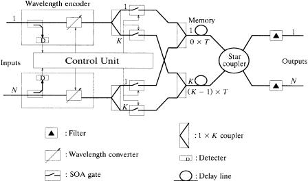
Duan et al. introduced a 16 16 photonic ATM switching architecture w11x, as shown in Figure 11.3, where each output port is assigned a fixed wavelength. This switch consists of three main blocks: wavelength encoding block, spatial switch block, and wavelength selection block. In the wavelength encoding block, there are N wavelength converters, one per input, each being tuned to the destined output port. When a cell arrives, a small fraction of the optical signal power is tapped by a coupler and sent to the electronic control unit, which processes the routing information of the cell. In a specific cell time slot, cells destined to different outputs are tuned to different wavelengths. These cells with different wavelengths are routed through the shortest path, which is selected by the SOA gates in the spatial switch. The spatial switch block contains K fiber delay lines to store the payloads of the cells for contention resolution. Each fiber delay line can store up to N different wavelengths. In the wavelength selection block, in each cell slot time, multiple wavelengths are broadcast to all output ports by a star coupler. There is a fixed-wavelength filter at each output port. These filters select the cells associated with their wavelengths and send them to the corresponding output ports.
284 OPTICAL PACKET SWITCHES
Fig. 11.3 Architecture of the ATM wavelength routing system.
This switch cannot perform multicast functions, because of the fixed-wave- length filters at the output ports. Furthermore, if there is more than one cell destined to the same output port, an arbitration mechanism is necessary in order to assign the incoming cells with the same wavelength to different fiber delay lines. Such a requirement increases the control complexity. In order to meet the cell loss requirement, more fiber delay lines are necessary. Moreover, the electronic controller always has to monitor the status of fiber delay lines to preserve the cell sequence.
11.2OPTOELECTRONIC PACKET SWITCHES
For the optoelectronic packet switches, optical switching networks are used for interconnection and transmission between electronic input and output modules. Logical control, contention resolution, and packet storage are handled electronically.
11.2.1HYPASS
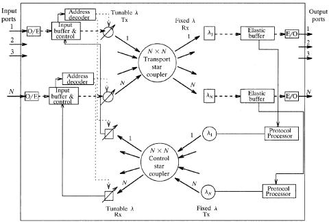
HYPASS w14x in Figure 11.4 is an optoelectronic hybrid cell switch in which electronic components are used for memory and logic functions, and optical components are used for routing and transporting data. In this figure, bold continuous lines represent optical paths, bold dashed lines represent serial data paths, dotted lines are tuning current paths, and thin continuous lines are control signal paths. The switch is composed of two networks: the transport network and the control network. The architecture is based on the broadcast-and-select approach in both of the networks. There is a unique
OPTOELECTRONIC PACKET SWITCHES |
285 |
Fig. 11.4 Global diagram of the HYPASS implementation. Ž 1988 IEEE..
optical wavelength associated with each of the output ports.As shown in Figure 11.4, the transport network has tunable-wavelength laser transmitters
at the input |
side, fixed-wavelength receivers at the output side, and |
an |
N N star |
coupler, which transfers the incoming data from inputs |
to |
outputs. In order to transfer control information from output ports to the input ports, a similar network is used.
When a cell arrives at an input port of the switch, first it is converted from optical to electronic and its destination address is obtained. Then the cell is temporarily stored in the corresponding input buffer. The tunable-wave- length laser transmitter of the corresponding input port is tuned to the wavelength of the requested output port. When a request-to-send signal Žor poll. is received from the corresponding output port via the control network, the cell is transmitted through the transport network. The acknowledgment representing successful delivery of the cell is also transmitted through the control network. If there are multiple cells for the same output port, contention occurs. Power threshold detection or multiple bit detection on the cell preamble could be used to detect collision. The cells which do not get acknowledgments in a slot time are kept to retry later. In order to resolve contention and provide successful transmission of cells, the tree-polling algorithm, which is explained in w14x, is employed in the selection of inputs in the following cell slots. The cells that reach the output ports successfully are stored in the elastic buffers and transmitted over the optical fiber trunks after the necessary electrical-to-optical conversion.
286 OPTICAL PACKET SWITCHES
The HYPASS architecture has advantages due to its parallel structure. However, since a slot time is based on the length of the polling step, transmission of a cell, and receipt of the acknowledgment, the time overhead for the electronic control and optical tuning operations are the factors limiting its capacity. The switch does not have multicasting capability, due to the use of fixed wavelength receivers at the output ports.
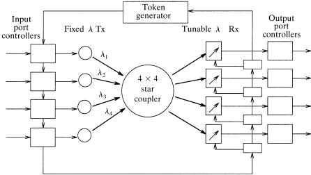
11.2.2STAR-TRACK
STAR-TRACK w15x is another hybrid switch architecture. It is based on a two-phase contention resolution algorithm. It also supports multicasting. As shown in Figure 11.5, the switch is composed of two internal networks: an optical star transport network, and an electronic control track surrounding the star network. The optical transport network has fixed-wavelength optical transmitters at the input port side, and wavelength-tunable optical receivers at the output port side. There is a unique wavelength associated with each input port. Input and output ports are connected through an optical star coupler. Output port conflicts are resolved by the ring reservation technique w16x. The electronic control network that implements the ring reservation technique is the major track linking input ports, output ports, and a token generator sequentially.
Cells arriving at the input ports are stored in the input buffers after optical-to-electronic conversion. There are two control phases in a cell transmission cycle. In the first phase, input ports write their output port requests into the tokens circulating in the control network. In the second
Fig. 11.5 STAR-TRACK architecture Žbasic single track..
OPTOELECTRONIC PACKET SWITCHES |
287 |
phase, the output ports read the tokens and tune their receivers to the appropriate input port wavelengths. Then, the cell transmission starts over the star transport network. The transmission and control cycles are overlapped in time in order to increase throughput. Since each input has a unique wavelength and there is input output port pair scheduling prior to transmission, cells are transmitted simultaneously without causing contention.
This architecture allows multicasting. However, the throughput of the switch may degrade as the number of multicasting connections increases, due to output port collisions in the first phase. It is shown that this problem can be alleviated by call splitting Ži.e., allowing a multicast call to be completed in multiple cell slots.. This architecture can support different priority levels for the cell by adding minor tracks into the control network. However, in that case, the token should recirculate among the input ports more than once, depending on the number of priority levels. This will increase the length of the write phase and result in longer cell processing time.
The main drawback of the switch is the sequential processing of the token by input and output ports. As a result, the time taken for the token to travel through the entire ring increases as the size of the switch increases. In the case of multiple priority levels, the recirculation period for the token becomes even longer. Here, HOL blocking is another factor that degrades throughput.
11.2.3Cisneros and Brackett’s Architecture
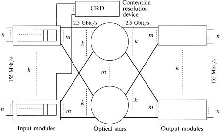
Cisneros and Brackett w17x proposed a large ATM switch architecture that is based on memory switch modules and optical star couplers. The architecture consists of input modules, output modules, optical star couplers, and a contention resolution de®ice ŽCRD.. Input and output modules are based on electronic shared memories. The architecture requires optical-to-electronic and electronic-to-optical conversions in some stages. Each output module has an associated unique wavelength. As shown in Figure 11.6, the input ports and output ports are put in groups of size n, and each group is connected to n m or m n memory switches, respectively. The interconnection between the input and output modules is achieved by k optical star couplers. There are k tunable laser transmitters and k fixed-wavelength receivers connected to each optical star coupler. In the Figure 11.6, for simplicity, the optical transmitters and receivers are not shown. The cells transmitted through the switch are buffered at the input and output modules. In the proposed architecture, input and output lines transmit cells at the rate of 155.52 Mbitrs. The lines that interconnect the input modules to the optical stars, and the optical stars to the output modules, run at 2.5 Gbitrs. The values of n, k, N, and m are 128, 128, 16,384, and 8, respectively.
The internal routing header of a cell is composed of two fields. One specifies the output module, and the other the port number in that output module. Each input module handles a single queue, in which the incoming
288 OPTICAL PACKET SWITCHES
Fig. 11.6 The switch architecture proposed by Cisneros and Bracket. Ž 1991 IEEE..
cells are kept in sequence. The input modules, the optical stars, and the output modules are connected as in a three-stage Clos network. However, the working principle is not the same as in the Clos network. Here, each input module sends the output module request of its HOL cell to the CRD. The CRD examines the requests, chooses one cell for each output module, and responds. The cells that won the contention are routed through the first k k optical star, and their HOL pointers are advanced. This process is repeated cyclically for each optical star. Cells at the output modules are kept in a sequence depending on which optical star they arrive in. In this architecture, all optical stars are kept busy if the CRD is m times faster than the time for cell transfer by the optical stars. The maximum number of optical couplers is determined from the time required to transfer a cell through an optical star and the time required by the CRD to resolve contention.
In the architecture, the time required for optical-to-electronic conversion, electronic-to-optical conversion, and tuning optical laser transmitters is not considered. All the calculations are mainly based on the time required to transfer a cell through an optical star. The output port contention resolution scheme is very complex, and the electronic controller can become a bottleneck. The switch does not have multicast capability, due to the fixed-wave- length receivers. Moreover, the maximum throughput of the switch is limited to 58% because of the HOL blocking w18x.