

Vankka J. - Digital Synthesizers and Transmitters for Software Radio (2000)(en)
.pdf
A Direct Digital Synthesizer with Tunable Delta Sigma Modulator |
277 |
board was built and a computer program was developed to control the measurement. The phase increment word and the other tuning signals were loaded into the test board via the parallel port of a personal computer. The block diagram of the test system is shown in Figure 14-7.
A spectrum plot of 12 MHz output from the DDS with real the tunable 1-bit ∆¦ D/A converter is illustrated in Figure 14-8. A spectrum plot of 20 MHz output from the DDS with the complex tunable 1-bit ∆¦ D/A converter is illustrated in Figure 14-9. The dynamic range is about 80 dB in the figures
14.8 Conclusions
The DDS with the tunable (real or complex) 1-bit ∆¦ D/A converter were designed and implemented. Since the 1-bit ∆¦ D/A converter has only one bit, the glitch problems and spurious noise resulting from the use of the multi-bit D/A converter are avoided. The main drawback of the DDS with the tunable ∆¦ D/A converter is that the broadband frequency switching speed is determined by the tuning time of the passband of the analog filter. The inband of the DDS with the tunable ∆¦ D/A converter could be placed anywhere in the Nyquist interval; it therefore gives a high degree of flexibility in frequency planning when the passband of the analog filter is fixed.
REFERENCES
[Ana02] "AD9744 14-Bit, 165 MSPS TxDAC D/A Converter," Analog Devices Data Sheet, May 2002.
[Azi95] P. M. Aziz, H. V. Sorensen, and J. Van der Spiegel, "Performance of Complex Noise Transfer Functions in Bandpass and Multi Band Sigma Delta Systems," in Proc. IEEE International Symposium on Circuits and Systems (ISCAS), 1995,Vol. 1, pp. 641-644.
[Fle98] FLEX 10K Embedded Programmable Logic Family Data Sheet, Altera Corp., San Jose, CA, Oct. 1998.
[Ftp] ftp://ftp.mathworks.com/pub/contrib/v5/control/delsig.tar.
[Iwa00] M. Iwamoto, A. Jayaraman, G. Hanington, P. F. Chen, A. Bellora, W. Thornton, L. E. Larson, and P. M. Asbeck, "Bandpass Delta-Sigma Class-S Amplifier," Electronics Letters, Vol. 36, No. 12, pp. 1010-1012,
June 2000.
[Jan02] I. Janiszewski, B. Hoppe, and H. Meuth, "Numerically Controlled Oscillators with Hybrid Function Generators," IEEE Transactions on Ultrasonics, Ferroelectrics and Frequency Control, Vol. 49, No. 7, pp. 995-1004, July 2002.

Chapter 15
15. A DIGITAL QUADRATURE MODULATOR WITH ON-CHIP D/A CONVERTER
A logical progression to the previous multi-standard modulator [Van02] and multicarrier work [Kos01] is to move the digital to analog interface even closer to the antenna in the base station transmitter structure. In traditional transmitters, a complex baseband signal is digitally modulated to the first IF (intermediate frequency) and then mixed to the second IF frequency and to the RF frequency in the analog domain. The first analog IF mixer stage of the transmitter can be replaced with the digital quadrature modulator presented in this chapter as shown in Figure 15-1. The two complex modulators are in series with the quadrature modulator as shown in Figure 15-2. In the digital complex modulators, the baseband in-phase (I) and quadrature (Q) channels are modulated onto orthogonal carriers (X Y) at the IF frequency at the lower sampling rate [Van02], [Kos01]. The tunable complex modulator, steered by the carrier NCO, enables the fine tuning of the transmitted carrier frequency with sub-Hz resolution [Van02], [Kos01], whereas this digital quadrature modulator is used for the coarse tuning. It is beneficial to implement the fine tuning at lower sampling frequencies and the coarse tuning at the higher frequencies, because of the smaller amount of hardware associated with the coarse tuning implementation. The quadrature modulator interpolates orthogonal input carriers by 16 and performs a digital quadrature modulation at carrier frequencies f /4, -f
 /4, f
/4, f /2 (f
/2 (f is the sampling frequency). It allows the quadrature modulation to be performed in the digital domain with high precision and perfect I/Q-channel matching. The major limiting factor of digital IF modulator performance at base station applications is the D/A converter, because the development of D/A converters does not keep up with the capabilities of digital signal processing with faster technologies [Van01].

 (
( (
(
 and
and 

 equal to 0, 1/2, 1/4, -1/4 in Table 4-2
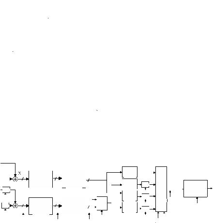
A Digital Quadrature Modulator with on-chip D/A Converter |
281 |
modulation in (15.2). Instead, multiplexers (MUXs) and negators (NEGs) can be used.
15.2 Interpolation Filters
The in-phase and quadrature-phase parts of the carriers from two complex modulators can be summed in the digital quadrature modulator (Figure 15- 3), which allows the formation of the multi-carrier signal. The sampling rate of the input samples is first increased by four with two halfband interpolation filters as shown in Figure 15-3. The passband of the first half-band filter restricts the maximum output frequency of the complex modulator in Figure 15-2 to about two-fifths of the input sampling rate of the quadrature modulator. The last filter has an interpolation ratio of 4, therefore the polyphase decomposition has four polyphase filters. The quadrature modulation in (15.2) for f ut/f
ut/f equal to 0, 1/2, 1/4, -1/4 (see Table 4-2) can be performed by negators in the polyphase filter outputs and 4:1 MUX as shown in Figure 15-3. In the lowpass mode f
 ut /f
ut /f = 0 in (2)), the output consists only of in-phase car-
riers (see Table 4-2). Therefore, only the X samples are driven to the polyphase filters. This is selected by the mode signal illustrated in Figure 15-3. Furthermore, the negators are disabled in the lowpass mode. In the bandpass mode (f ut/f
ut/f = 1/4 or f
 ut/f
ut/f = -1/4 in (15.2)), the output consists of the inter-
leaved X and Y samples (see Table 4-2). Furthermore, every other second X and Y sample is negated. Therefore, the X samples are driven to the first and third polyphase filter and Y samples to the second and fourth polyphase filter. The third or fourth polyphase filter outputs are negated. The quadrature modulation by f ut /f
ut /f = 1/4 or f
 ut /f
ut /f = -1/4 can be performed by selecting whether to negate the Y-branches or not (control signals CTR4 and CTR5 in Figure 15-3). In the highpass mode (f
 ut/f
ut/f = 1/2 in (15.2)), the output consists
only of in-phase carriers and every second sample is negated (see Table 4-2). Therefore, the X samples are driven to the polyphase filters, and the second and fourth of the polyphase filter outputs are negated.
The digital quadrature modulator interpolates input carriers by 16. Therefore, the transition band for the analog reconstruction filter is increased and
X1 |
|
|
|
|
|
|
|
|
|
|
|
|
|
|
|
|
|
|
|
|
|
h4k |
|
|
|
|
|
|
|
16 |
1st Half- |
16 |
2nd Half- |
16 |
|
8 taps |
|
|
|
|
|
X2 |
|
band Filter |
|
band Filter |
|
h |
4k+ 1 |
|
|
|
D/A |
||
|
|
|
(43 taps) |
|
(23 taps) |
|
|
7 taps |
NEG |
4:1 |
12 |
||
Y |
|
NEG |
|
|
|
|
Conver- |
||||||
1 |
|
|
|
|
|
h4k+2 |
CTR1 |
MUX |
|
||||
|
|
|
|
|
|
|
|
ter |
|||||
|
|
|
|
|
|
|
|
NEG |
|
|
|||
|
|
CTR4 |
|
|
|
|
|
7 taps |
|
|
|
||
|
|
1st Half- |
|
2nd Half- |
|
|
|
fs |
|
|
|||
Y2 |
Y 16 |
16 |
16 |
MUX |
h4k+3 |
CTR2 |
|
fs |
|||||
NEG |
band Filter |
|
band Filter |
|
|
||||||||
|
|
|
|
||||||||||
|
|
CTR5 |
(43 taps) |
|
(23 taps) |
|
|
7 taps |
NEG |
|
|
|
|
|
|
|
|
|
|
|
|
|
|
|
|||
|
|
|
|
|
|
|
Mode |
|
|
CTR3 |
|
|
|
|
|
fs/16 |
|
fs/8 |
|
fs/4 |
|
|
|
|
fs/4 fs/2 |
|
|
|
|
|
Figure 15-3 . Digital quadrature modulator in Figure 15-2 |
|
|
||||||||


 . The images related to the last interpolation stage are shown in Figure 15-5. The image selection is achieved by changing the filter passband.


