

Chapter 6 - Wiring Techniques
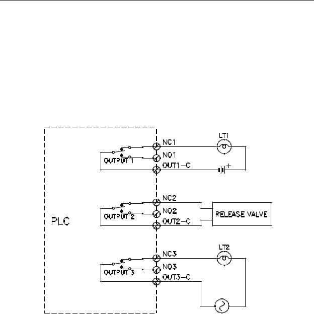
which has it's own DC power source. Notice that lamp LT1 will be lit whenever OUTPUT
1 is turned OFF. This could possibly be a fault indicator for the system. Lamp LT2 is an AC lamp having it's own AC source. LT2 is also lit when OUTPUT 3 is turned OFF. This could be used as a fault indication. OUTPUT 2 is connected to a release valve which has an internal power source and only needs a contact closure to release. In this case, the release valve is connected to the normally closed terminal for OUTPUT 2. This connection provides for the release valve to be in the release condition should the PLC lose power. This may be the requirement to provide for the machine being in a safe condition in case of system failure. Notice that in the wiring of INPUT 1 and INPUT 3, the wiring provides for a power source, switch and light all in series, with the switch controlling the flow of current to the light.
Figure 6-14 - Isolated Contact Wiring
6-8. Solid State Outputs
There are several types of solid state outputs available with PLC's. Three popular types are transistor, triac and TTL. All three of these output units will generally have a common terminal although triac output units are available in an isolated configuration.
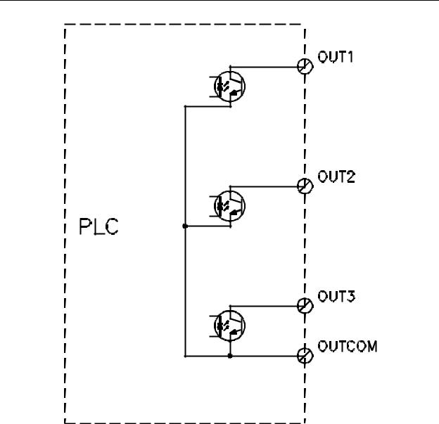
Transistor output units are usually open collector with the common terminal connected to
6-17

Chapter 6 - Wiring Techniques
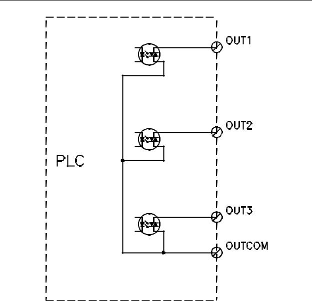
the emitters of all outputs. A transistor output unit providing three open collector outputs is shown in Figure 6-15. In most, if not all transistor output units, the transistors optically isolated from the PLC. The transistors shown in Figure 6-15 are optically isolated devices. This unit has all the emitters of the output transistors connected to one common terminal labeled OUTCOM. The transistors contained in this unit are NPN although PNP units are available. There are two different types of transistor units available and they are described as sourcing and sinking. The NPN units are referred to as sinking and the PNP units as sourcing. The unit shown in Figure 6-15 contains sinking outputs. This means that the transistor is configured to sink current to the common terminal, that is, the outputs will have current flow into the terminal.
6-18
Chapter 6 - Wiring Techniques
Figure 6-15 - Transistor Output Unit
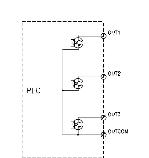
A sourcing type output will have current flow out of the terminal. Another way of looking at the difference is that a sinking output will pull the output voltage in a negative direction and the sourcing output will pull the output voltage in a positive direction. The sourcing and sinking description conforms to conventional current flow from positive to negative. A sourcing transistor output unit is shown in Figure 6-16. Notice that the transistors used are PNP type and that the common terminal would have to be connected
6-19
Chapter 6 - Wiring Techniques
to the positive terminal of the power supply for the transistor to be properly biased. This will cause the outputs to be pulled in a positive direction when the transistor is turned ON (a sourcing output).
Figure 6-16 - Transistor Sourcing Output
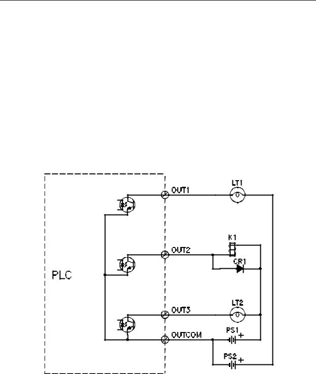
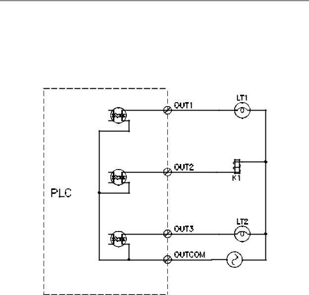
A wiring diagram for a transistor sinking output unit is shown in Figure 6-17. This diagram shows three output devices connected to the output unit. Lamp LT1 will light when OUTPUT 1 turns ON since the output transistor will saturate when the output turns ON. The saturated transistor will sink current to the OUTCOM terminal causing current to flow
6-20
Chapter 6 - Wiring Techniques
in the lamp. OUT2 is connected to a coil K1. This could be a solenoid or relay. This device will be energized when OUTPUT 2 is turned ON causing the output transistor to saturate. Notice that a diode, CR1, is connected across K1 in such a manner as to be normally reverse biased. This diode prevents excessive voltage buildup across K1 when the output transistor turns OFF. When the output transistor turns OFF and the magnetic field in the coil begins to collapse, a voltage in opposition to the applied voltage is developed. Unchecked, this voltage could be as high as several hundred volts. A voltage this high would quickly destroy the output transistor. The voltage is not allowed to build up because the current developed by the collapsing field is shunted through the diode.
Transistor output units now generally have this diode built into the output unit for protection. Also, some relays are manufactured with this diode installed. Notice, too, that the diagram of Figure 6-17 includes two separate power sources, one providing power for LT1 and the other providing power for K1 and LT2. This is a typical situation since there may be occasions when devices connected to the output unit operate at different voltages. In this case, LT1 could be a 5 volt lamp and LT2 and K1 could be 24 volt devices. The only requirement is that the two power supplies (PS1 and PS2) must have a common negative terminal that is connected to the OUTCOM terminal.
Figure 6-17 - Transistor Output Wiring
6-21

Chapter 6 - Wiring Techniques
Figure 6-18 contains the schematic drawing for a triac output unit. All output triacs have one common terminal which will be connected to one side of the AC power source providing power for the output devices being controlled. Each triac is triggered when the output associated with it is turned ON. There are units available that have zero crossover networks built in to provide for noise reduction by only allowing the triac to turn ON at the time the power signal crosses through zero volts. Noise and current spikes can be generated when the triac turns ON if the AC voltage is at some voltage other than zero since the voltage to the output device being controlled will instantly go from zero with the triac OFF to whatever the AC value of the voltage is at turn-on. If the triac turns ON at the time the AC voltage is passing through zero volts, no such spikes will be produced. Notice that the triac outputs shown in Figure 6-18 are optically isolated from the PLC. This allows the PLC to control very high voltage levels (120 - 240 VAC) with isolation of these voltages from the low voltage circuitry of the PLC.
6-22
Chapter 6 - Wiring Techniques
Figure 6-18 - Triac Output Unit
Figure 6-19 contains the wiring diagram for a triac output unit. As can be seen in the diagram, the common terminal for the triacs is connected to one side of the AC source powering the output devices controlled by the unit. Output units are available with different voltage and current ratings. The devices being controlled by the output unit shown in Figure 6-19 look the same as the ones in Figure 6-17. The difference is that all devices in
Figure 6-17 are DC units and all devices in Figure 6-19 operate on AC. Also notice that the diode across K1 is not present in the triac output unit drawing. This is because the triac
6-23
Chapter 6 - Wiring Techniques
turns OFF when the applied current crosses through zero volts. The result is that either a very small magnetic field is present or no magnetic field is present when the triac turns OFF and the voltage spike present in a DC system is not generally a problem. This can still be a problem if the coil is highly inductive because the voltage and current will be so far out of phase that some voltage will still be present when the current crosses zero. In this case a series combination of resistance and capacitance is connected in parallel with the coil. This series R-C circuit is referred to as a snubber. The terminal of the AC source generally connected to the common terminal of the output unit is the neutral lead of the source.
Figure 6-19 - Triac Output Wiring
Figure 6-20 shows the schematic diagram of an output unit containing three TTL outputs. Notice that these outputs are also optically isolated. In some cases these may be direct and not optically isolated but the isolated units provide better protection for the PLC. The outputs of the TTL unit have a common terminal (OUTCOM) which must be connected to the negative terminal of the power supply for the external TTL devices being driven by the output unit. Some TTL output units require that the 5 VDC power for the output circuitry be connected to the output unit to also provide power for it's internal TTL circuitry. The connection of these outputs to external TTL circuitry would be the same as
6-24
Chapter 6 - Wiring Techniques
with any other TTL connections. The only concern with these outputs is that various PLC manufacturers specify the outputs as positive or negative logic. How this is handled in the ladder diagram will be affected by this specification.
Figure 6-20 - TTL Output Unit
As can be seen from the above discussion of input and output units, there are a large variety of options available. Wiring for each type of unit is critical to the unit's proper operation. Much care must be taken to insure proper operation of the output or input unit without causing damage. Also, there are safety concerns which must be addressed when
6-25

Chapter 6 - Wiring Techniques
planning and implementing the wiring of the system to provide for a system that will not be a hazard to the people operating and maintaining it.
6-26

Chapter 6 - Wiring Techniques
Chapter 6 Review Questions and Problems
1.Draw the input wiring diagram for a PLC system using a 24 VDC input unit with the following inputs:
IN1 - Normally open pushbutton ON switch
IN2 - Normally open pushbutton OFF switch
IN3 - Normally closed selector switch labeled STEP 1 / STEP 2
IN4 - Normally open footswitch
Show all switches using the correct drawing symbol and show all devices including the power supply. The PLC being used does not hav an internal
24VDC power supply.
2.If one terminal of a lamp is connected directly to the negative terminal of the power supply, what kind of transistor output unit will be required (sourcing or sinking) to allow the PLC to light the lamp?
3.The negative lead of a power supply is connected directly to one lead of a coil. Draw the wiring diagram for the proper connection of the coil to a transistor output unit. Also, show the spike protection diode across the coil.
4.Using a relay output unit with one FORM C contact driven from OUTPUT 1, draw the wiring diagram for a system with two AC powered lamps, one that will light when OUTPUT 1 is ON and one that will light when OUTPUT 1 is
OFF.
5.Draw the wiring diagram for a system combining the requirements of problems 1, 2 and 3 above utilizing one power source wheich is not part of the PLC.
6-27