

ЛЕКЦИИ ФШФС_2007 / НАШИ СТАТЬИ / JCTE477_РЭ_5_05_Англ
.pdfNONDESTRUCTIVE QUALITY CONTROL OF INTEGRATED CIRCUITS |
497 |
Figure 17 compares the normalized power spectral density SE = SV/ V20 of equilibrium 1/f noise for type-2 resistors under dc driving (Vp = V0 = 5 V) and the nor-
malized power spectral density SN = SU/ U2dc of non-
equilibrium 1/f noise for the film contacts under pulsed test signal [24]. Notice that the two noise components differ markedly in magnitude; for example, at 10 Hz, SN is higher than SE by more than three orders of magnitude, which indicates a strong effect of noise on Udc. However, it turned out that at V0 ≤ 5 V nonequilibrium fluctuations in contact conductance make an insignificant contribution to the total 1/f noise of the resistor. As can be deduced from Fig. 17b, the frequency exponent γ is 0.7 to 0.9 for the nonequilibrium 1/f noise and is 1 to 1.2 for the equilibrium flicker noise [24, 29].
Zhigal’skii and Karev [73] reported the effect of temperature variation on the 1/f noise of Ta thin-film resistors. Equilibrium and nonequilibrium flicker noise were measured under dc and pulsed signals, respectively, at Vp = V0 = 5 V over the temperature range 300–400 K. The equilibrium and nonequilibrium noise have been found to increase and decrease, respectively, with increasing temperature. The latter effect is due to a decrease in contact resistance. The former can be attributed to activation of mobile lattice defects (vacancies) in the resistive film (see Section 2B). These findings are further evidence that different mechanisms underlie the two types of flicker noise under the stated driving conditions. Note that at V0 ≤ 5 V the nonequilibrium noise is mainly produced by the film contacts rather than the resistive film.
Under dc driving below 105 A/cm2 , the 1/f noise of a resistive film is mainly caused by fluctuations in resistance: see the term R0(t) of Eq. (19). By contrast, fluctuations in the dc voltage component, which are responsible for nonequilibrium flicker noise, are related to fluctuations in N(I, t), which are mainly caused by fluctuations in R1(t) (see Eqs. (13), (15)).
Osokin [70] identified the respective nonlinear effects of the film contacts and resistive film on Udc. For resistors of type 2, the effect of the film contacts has been found to dominate in Udc and, hence, in the nonequilibrium flicker noise of film resistors.
The term R1 of Eq. (13) is responsible for a quadratic CVC, which stems from the nonlinear behavior of the film contacts. Zhigal’skii and Zaitsev [69] showed this in an experiment where sinusoidal driving (see Section 3B) was used to examine the nonlinear CVC of the resistors shown in Fig. 16. It has been found that the resistive film is characterized by a cubic CVC, whereas the film contacts are characterized by a quadratic CVC. In particular, this applies to resistors of type 2.
Figure 18 presents graphs of the thirdand the sec- ond-harmonic amplitude for the voltage response of a square resistive film and a film contact, respectively, with the harmonic amplitudes plotted against the amplitude
U3 , µV |
|
|
|
|
U2c × 10, µV |
|
|
||||||||
12 |
|
(a) |
|
|
1 |
14 |
|
|
(b) |
1 |
|||||
|
|
|
|
||||||||||||
|
|
|
|
|
|||||||||||
|
|
|
|
|
|
2 |
|||||||||
|
|
|
|
|
|
|
|
|
|||||||
8 |
|
|
|
|
|
|
|
12 |
|
|
|
|
|
||
|
|
|
|
|
|
|
|
|
|
|
|
3 |
|||
|
|
|
|
|
|
|
|
|
|
||||||
|
|
|
|
|
|
|
|
|
|
|
|
||||
|
|
|
|
|
|
|
|
|
|
|
|
|
|||
|
|
|
|
|
|
|
|
|
|
|
|
|
|||
|
|
|
|
|
|
|
|
|
|
|
|
|
|
||
4 |
|
|
|
|
|
2 |
10 |
|
|
|
|
|
|
|
|
|
|
|
|
|
|
|
|
|
|
|
|
||||
|
|
|
|
|
|
|
|
|
|
||||||
|
|
|
|
|
3 |
8 |
|
|
|
|
|
|
|
||
|
|
|
|
|
|
|
|
|
|
|
|
||||
|
|
|
|
|
|
|
|
|
|
|
|
||||
|
|
|
|
|
|
|
|
|
|
|
|
|
|
|
|
|
|
|
|
|
|
|
|
|
|
|
|
|
|
|
|
|
|
|
|
|
|
|
|
6 |
|
|
|
|
|
|
|
|
|
|
|
|
|
|
|
|
|
|
|
|
|
|
|
|
|
|
|
|
|
|
|
|
|
|
|
|
|
|
|
|
|
|
|
|
|
|
|
|
|
|
|
|
|||
0 |
|
|
|
5 |
10 |
0 |
5 |
10 |
|||||||
U1, V
Fig. 18. (a) Thirdand (b) second-harmonic amplitudes vs. fundamental-component amplitude for the voltage response of (a) a square resistive film and (b) a film contact [69]. In each panel curves 1–3 refer to resistors of type 1 (rapid deposition), 2 (slow deposition), and 4 (two-staged deposition), respectively.
U1 of the fundamental frequency component [69]. The curves in each panel refer to different types of resistors. It is seen that resistive films produced at a high deposition rate display the strongest nonlinearity and the highest level of 1/f noise [24].
Physically the cubic nonlinearity of type-1 resistive films is attributable to vacancy creation and annihilation [6]. This explanation is supported by the higher levels of 1/f noise and the third-harmonic amplitude observed in rapidly deposited films, in which case vacancies have no time to reach the film surface in the course of deposition [74]. During the useful life of the resistor, the excess vacancies can conglomerate into complexes, thus forming microscopic pores and voids [1, 28, 74]. When current is passed through such a film, its density is higher at these inhomogeneities, leading to destructive local overheating.
Figure 18b indicates that for any U1 the nonlinear behavior of film contacts is also greatly influenced by process conditions. Note that the second-harmonic distortion is the most accurate characteristic of film contacts [69]. The film contacts produced at a high deposition rate display the strongest nonlinearity and the highest level of 1/f noise.
Both of the harmonic amplitudes grow with U1 . It has been found for all the resistors that at U1 = 10 V the secondand third-harmonic amplitudes of the film contacts are more than ten times higher those of the resistive film while the contact resistance accounts for less than 0.5% of the total resistance [69]. Thus, if a film resistor carries a high current, its film contacts can contribute significantly to the secondand third-harmonic distortions and to the nonequilibrium flicker noise while making a relatively small contribution to the total resistance.
JOURNAL OF COMMUNICATIONS TECHNOLOGY AND ELECTRONICS Vol. 50 No. 5 2005
498 |
ZHIGAL’SKII |
Ueff, arb. units
16 |
|
|
|
|
|
12 |
|
|
|
|
|
8 |
|
|
|
|
|
4 |
|
|
|
|
|
0 |
4 |
6 |
8 |
10 12 14 16 |
18 20 22 24 26 28 |
2 |
Item no.
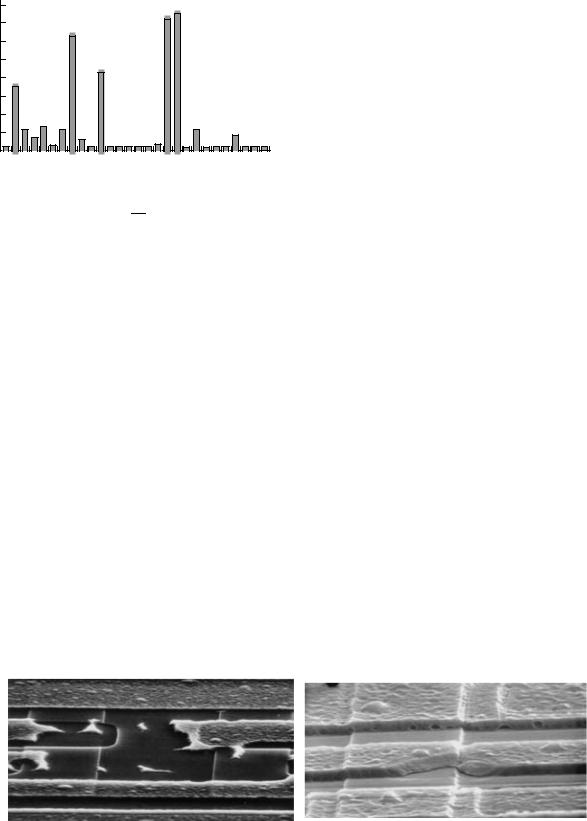
Fig. 19. Current-consumption noise measurements on
RAM ICs (537RU6 series) at CE = 0: the column diagram of effective noise voltage (1–8 Hz) over a sample [76]. The ICs are powered at 4.0 V.
The nonequilibrium flicker noise that arises at the interface between a resistive and a metal film or between two metal films results from chemical reactions between adsorbed gases and the material or from oxidation during fabrication and storage.
Accordingly, the nonlinear response and nonequilibrium flicker noise of film contacts should involve electrical transport across a thin oxide layer at the interface between a film contact and a resistive film [1, 27, 28]. The electrical transport may proceed by overcoming the potential barrier or by tunneling, and it should produce a second-harmonic component and enhance a third-harmonic one. The nonequilibrium flicker noise may be linked to fluctuations in barrier height [75]. In the case of low-quality contacts, such fluctuations may dominate the nonequilibrium flicker noise of film resistors. If these are fabricated without breaking vacuum, there is no oxide at the contact and, hence, the lowest levels of harmonic distortion and nonequilibrium flicker noise in the film contacts.
Nonequilibrium flicker noise at contacts may also be produced by creation and annihilation of excess vacancies and by mechanical stress [9].
The above results show that it is not always possible to assess the quality of film resistors and their film contacts by equilibrium flicker noise measured under dc conditions. This problem may be solved by measuring nonequilibrium noise and harmonic distortions (the second and third ones). Note that this approach allows one to test the resistive film and film contacts separately during fabrication or finished-product testing.
6. OVERALL TESTING OF LSICs AND ELECTRONIC DEVICES BY FLUCTUATIONS
IN THE CONSUMPTION CURRENT
In order to attain a high reliability of modern CMOS LSICs and VLSICs operating in long-term performance electronic facilities, it is necessary to conduct an additional testing that reveals potentially unreliable ICs and latent defects in their structure. The steadily increasing VLSIC integration level and, especially, the shift in chip design technology into the depth of the submicrometer range substantially hamper checking ICs for macroscopic defects.
Measurement of current-consumption noise, i.e., LF fluctuations in current consumption under static conditions, has proven an effective method for detecting and identifying latent defects in CMOS LSICs and VLSICs, as well as for predicting the overall circuit reliability [3, 76, 77]. In this approach an IC being tested is treated as a one-port network; ICs are treated the same way during noise measurements for passive circuit elements.
Current-consumption noise in CMOS circuits is commonly attributed to the electronic surface states and oxide traps present in MOS structures [75]. However, with a complex arrangement of circuit elements, macroscopic defects in CMOS circuits also have an important role in current-consumption fluctuations. The question thus arises as to how to discriminate this noise component from the fundamental noise components: thermal, shot, and phonon-scattering 1/f noise (see Sections 1, 2). The noise in the IC feed circuits contains such basic components as thermal and shot noises and the 1/f noise caused by fluctuations in the mobility of
(a) |
(b) |
Fig. 20. Photographs of latent defects detected by measurement of current-consumption noise: (a) an electrocorrosion-induced open fault [76] and (b) an oxide-step interconnection fault (middle path) [60].
JOURNAL OF COMMUNICATIONS TECHNOLOGY AND ELECTRONICS Vol. 50 No. 5 2005

NONDESTRUCTIVE QUALITY CONTROL OF INTEGRATED CIRCUITS |
499 |
current carriers scattered by phonons (see Sections 1 and 2), as well as an additional component associated with fluctuations in the consumption current that are caused by macroscopic defects in the LSIC structure. Detection and identification of this component of LF noise forms the basis of the LSIC diagnostic quality control using observations of LF fluctuations of current Icc flowing in the feed circuit.
Zhigal’skii and Gal’chenko [3] and Gal’chenko and Zhigal’skii [76] investigated current-consumption noise in commercial RAM ICs. The items examined conformed to specifications but were taken from a batch of subnormal yield.
In the latter study, the power spectral density of cur- rent-consumption noise was found to vary as 1/f γ [76], where γ ranged from 0.9 to 1.2, depending on the item. To rapidly estimate the noise level, effective noise voltage Ueff was measured over the frequency range 1−8 Hz.
Figure 19 depicts the column diagram of Ueff over a sample of 28 items when the chip-enable signal is set to
CE = 0 and the ICs are powered at 4.0 V, the minimum allowable level [76].
Notice that some items differ in Ueff by one or two orders of magnitude; this difference will increase with
power-supply voltage. Almost the same noise level was
observed at CE = 1 [76]. Such a wide spread in Ueff suggests that items showing intense noise may contain latent defects.
Indeed, close inspection of such chips revealed defects typical of CMOS technology: structural faults in polysilicon resistors, electrocorrosionand elec- tromigration-induced degradation of Al films, loss of contact, open faults on oxide steps, field-oxide cracking, and defects leading to junction or gate-oxide breakdown [3, 76].
Figure 20 displays photographs of an electrocorro- sion-induced open fault (Fig. 20a) and an oxide-step interconnection fault (Fig. 20b) that have been detected by current-consumption noise measurement [76, 60].
Some items exhibited RTS noise in current consumption (see Section 1). This pattern was found to be indicative of open faults at oxide steps or poor ohmic contact in contact windows. This pattern occurs even for a single fault of such type. The measured characteristic time τ0 of the faults (see Section 1F) varies from fractions of a second to tens of minutes, depending on the constants of the circuits involved.
Current-consumption noise measurement enables one to detect, identify, and locate oxide-step open faults and loss of contact. It takes considerable time to detect the faults by conventional methods, and it is impossible to detect them by IDDQ testing [78].
Current-consumption noise measurement is also useful in the case where an accepted item works according to specification for a specific length of time
(fractions of a second to tens of minutes) before a failure occurs that persists until the power is turned off; this pattern repeats if power is turned on after a sufficiently long break. The failure mode is observed in some static RAM CMOS circuits [79, 80]. Current-consumption noise in such circuits has an RTS character. An inspection has identified the underlying fault as loss of contact in one contact window.
With respect to the above-mentioned faults, Gal’chenko and Zhigal’skii [77] proposed a resistor of 106 Ω and a capacitor of 0.01 pF in parallel as a model of an oxide-step open fault at the drain of a p-channel MOSFET used in a CMOS memory cell. This model was validated by computer simulation of current-con- sumption noise with DesignLab [81]. Close agreement with the experiment was achieved.
With a normal power-supply voltage, a sharp increase in current-consumption noise or the appearance of RTS pattern can be regarded as an early sign of breakdown in a p–n junction or gate oxide (see Section 4E). This phenomenon is well understood [75, 82–85]. The variation of Ueff with power-supply voltage for LSICs in this case is similar to those for MOS structures containing a defect that causes soft breakdown. Thus, elevated cur- rent-consumption noise exhibited by inferior items at an allowable power-supply voltage can be used for screening [76]. Note that the CVCs of the tested items demonstrate an anomalous behavior only at voltages exceeding the maximum allowable level (–5.5 V).
Nondestructive testing according to the level and pattern of current-consumption noise can also be applied to systems comprising tens to hundreds of ICs. For example, the defective LSI circuit of Fig. 20a was identified in a unit containing about 20 ICs [76], despite the fact that the circuit conformed to specifications.
To obtain a comprehensive picture, testing of cur- rent-consumption noise should be performed in conjunction with certain stress procedures. This strategy is essentially nondestructive, and it does not affect the reliability of items being tested.
To summarize, measurement and analysis of cur- rent-consumption fluctuations under static conditions enable one to detect and identify latent defects in passive elements of ICs (metallization patterns, contact pads, vias, etc.) that cannot be detected by conventional methods. As elevated current-consumption noise represents an early sign of different types of catastrophic failure, it can be employed in screening.
7. CONCLUSIONS
The major mechanisms of 1/f γ noise (flicker noise) in metal films and contacts are as follows. Carriermobility fluctuations due to phonon scattering are manifested in fundamental equilibrium 1/f noise. The number fluctuations of quasi-equilibrium vacancies in the absence of current underlie vacancy-induced equilibrium 1/f noise. Electric current, ionizing irradiation,
JOURNAL OF COMMUNICATIONS TECHNOLOGY AND ELECTRONICS Vol. 50 No. 5 2005
500 |
ZHIGAL’SKII |
mechanical stress, etc., can cause nonequilibrium 1/f γ noise. Which of the mechanisms dominate is determined by the microstructure of the specimen and the external conditions (current and temperature). In metal films, equilibrium 1/f noise and electromigration 1/f 2 noise often coexist, but the latter tends to show up at high currents and low frequencies (on the order of 10−4 Hz).
Nonequilibrium flicker noise is closely related to nonlinear electrical transport. If the CVC of a specimen is approximated by a polynomial, nonequilibrium 1/f γ noise corresponds to fluctuations of the CVC terms on an order greater than one; these terms can dominate the total 1/f noise at sufficiently high currents. The level and character of noise are determined by the mechanism of carrier transport and scattering.
Metal films and contact joints may contain, as a result of gas adsorption, inclusions in the form of thin dielectric layers at grain boundaries or interfaces. In this case, the nonequilibrium noise component may dominate even at current densities lower than 104 A/cm2. Measurements of 1/f noise on Ta thin-film resistors have revealed that the contact pads may be the major contributor to the total nonequilibrium flicker noise, although they have an insignificant influence on the total resistance.
The magnitude of nonlinearity in the CVC and the level of nonequilibrium 1/f γ noise are useful for quality control because they can yield clues about lattice defects and disturbances such as excess vacancies, dislocations, inclusions (e.g., dielectric layers), strained regions, pores, and cracks. These are responsible for local overheating during operation.
In this review techniques have been discussed for extracting nonequilibrium flicker noise from total 1/f noise in the case of weakly nonlinear fast-response oneport passive networks. These methods may be used to examine fluctuations in the passive parts of practicable ICs, such as metal films, contact joints, resistors, and vias. They are also useful for nondestructive testing. Nonequilibrium flicker noise should be measured under pulsed rather than sinusoidal driving because this approach is easier to implement, is very sensitive to latent defects, and can be used in IC manufacture.
Nonequilibrium flicker noise, but not equilibrium flicker noise, can provide data on latent defects in conducting films and contacts. It can be employed in nondestructive testing of passive elements, particularly film resistors. At the same time, vacancy-induced equilibrium 1/f noise and harmonic distortions can serve to predict electromigration immunity, the long-term reliability of metal–semiconductor ohmic contacts, and the strength of gold-wire bonds.
Defects in metallization patterns and contact joints also affect the level and pattern of current-consumption noise in circuits and systems. The noise can be used to detect and identify latent defects in ICs. In particular,
digital ICs exhibiting elevated current-consumption noise under static conditions can be regarded as inferior in reliability. Close inspection of such chips reveals defects such as electrocorrosionor electromigrationinduced degradation of metallization patterns, open faults on oxide steps, loss of ohmic contact, field-oxide cracking, and defects leading to junction or gate-oxide breakdown. The testing of current-consumption noise under static conditions can be employed in screening of digital CMOS circuits.
REFERENCES
1.G. P. Zhigal’skii and B. K. Jones, The Physical Properties of Thin Metal Films (Taylor & Francis, New York, 2003).
2.B. K. Jones, in Adv. Electron. Electron Phys. (1994), Vol. 87, p. 201.
3.G. P. Zhigal’skii and V. R. Gal’chenko, in Proceedings of the 17th International Conference on Noise and Fluctuation, Brno University of Technology, Brno, Czech Republic, 2003, Ed. by J. Sikula (World Sci., Singapore, 2003), p. 749.
4.A. Touboul, F. Verdier, and Y. Herve, in Proceedings of the International Conference on Noise in Physical Systems and 1/f Fluctuations, Kyoto, Japan, 1991, Ed. by T. Musha, S. Sato, and M. Yamamoto (IOS, Tokyo, 1992), p. 73.
5.A. van der Ziel, Fluctuation Phenomena in Semiconductors (Butterworths Scientific, London, 1959; Inostrannaya Literatura, Moscow, 1961).
6.G. P. Zhigal’skii, Usp. Fiz. Nauk 87 (6), 201 (1997).
7.J. Caro, in Proceedings of the 13th International Conference on Noise in Physical Systems and 1/f Fluctuations, Palanga, Lithuania, 1995, Ed. by V. Bareikis and R. Katilius (World Sci., Singapore, 1995), p. 41.
8.R. F. Voss and J. Clark, Phys. Rev. Lett. 36, 42 (1976).
9.G. P. Zhigal’skii, Usp. Fiz. Nauk 173, 465 (2003).
10.B. Neri, A. Diligenti, and P. E. Bagnoli, IEEE Trans. Electron Devices 34, 2317 (1987).
11.B. Neri, C. Ciofi, and V. Dattilo, IEEE Trans. Electron Devices 44, 1454 (1997).
12.F. N. Hooge and A. M. H. Hoppenbrouwers, Physica (Utrecht) 45, 386 (1969).
13.F. N. Hooge, Physica B (Amsterdam) 83, 14 (1976).
14.F. N. Hooge, in Proceedings of the 14th International Conference on Noise in Physical Systems and 1/f Fluctuations, Leuven, Belgium, 1997, Ed. by C. Claeys and E. Simoen (World Sci., Singapore, 1997), p. 3.
15.T. Musha, in Proceedings of the 15th International Conference on Noise in Physical Systems and 1/f Fluctuations, Polytechnic University, Hong Kong, China, 1999, Ed. by C. Surya (Bentham, London, 1999), p. 18.
16.B. S. Bokshtein, Diffusion in Metals (Metallurgiya, Moscow, 1978) [in Russian].
17.L. A. Girifalco, Statistical Physics of Materials (WileyInterscience, New York, 1973; Mir, Moscow, 1975).
JOURNAL OF COMMUNICATIONS TECHNOLOGY AND ELECTRONICS Vol. 50 No. 5 2005
NONDESTRUCTIVE QUALITY CONTROL OF INTEGRATED CIRCUITS |
501 |
18.V. V. Potemkin, I. S. Bakshi, and G. P. Zhigal’skii, Radiotekh. Elektron. (Moscow) 28, 221 (1983).
19.A. van der Ziel, Noise: Sources, Characterization, Measurement (Prentice Hall, Englewood Cliffs, N.J., 1970; Sovetskoe Radio, Moscow, 1973).
20.M. J. Buckingham, Noise in Electronic Devices and Systems (Ellis Horwood, Chichester, 1983; Mir, Moscow, 1986).
21.M. W. Thompson, Defects and Radiation Damage in Metals (Cambridge Univ. Press, Cambridge, 1969; Nauka, Moscow, 1983).
22.G. P. Zhigal’skii, Pis’ma Zh. Eksp. Teor. Fiz. 54, 510 (1991).
23.G. P. Zhigalskii, in Proceedings of the International Conference on Noise in Physical Systems and 1/f Fluctuations, Kyoto, Japan, 1991, Ed. by T. Musha, S. Sato, and M. Yamamoto (IOS, Tokyo, 1992), p. 39.
24.G. P. Zhigal’skii and A. V. Karev, Radiotekh. Elektron. (Moscow) 44, 220 (1999) [J. Commun. Technol. Electron. 44, 206 (1999)].
25.G. P. Zhigal’skii, Zh. Fiz. Khim. 69, 1355 (1995).
26.G. P. Zhigal’skii and B. K. Jones, in Proceedings of the 15th International Conference on Noise in Physical Systems and 1/f Fluctuations, Polytechnic University, Hong Kong, China, 1999, Ed. by C. Surya (Bentham, London, 1999), p. 172.
27.K. L. Chopra, Thin Film Phenomena (McGraw-Hill, New York, 1969; Mir, Moscow, 1972).
28.G. P. Zhigal’skii, Physical Phenomena in Metal Thin Films: A Tutorial for the Film Physics Course (MIET, Moscow, 1996) [in Russian].
29.B. K. Jones and G. P. Zhigal’skii, in Proceedings of the 16th International Conference on Noise in Physical Systems and 1/f Fluctuations, Gainesville, Fla., 2001, Ed. by G. Bosman (World Sci., Singapore, 2001), p. 73.
30.J. A. Schwarz, A. J. Patrinos, I. S. Bakshee, et al., J. Appl. Phys. 70, 1561 (1991).
31.T. M. Chen, in AIP Conference Proceedings 285: Noise
in Physical Systems and 1/f Fluctuations, Ed. by
P.H. Handel and A. L. Chung (AIP, New York, 1993), p. 17.
32.A. M.Yassine and T. M. Chen, in Proceedings of the 13th International Conference on Noise in Physical Systems and 1/f Fluctuations, Palanga, Lithuania, 1995, Ed. by
V.Bareikis and R. Katilius (World Sci., Singapore, 1995), p. 614.
33.C. Ciofi, A. Diligenti, and B. Neri, in Proceedings of the 13th International Conference on Noise in Physical Systems and 1/f Fluctuations, Palanga, Lithuania, 1995, Ed. by V. Bareikis and R. Katilius (World Sci., Singapore, 1995), p. 618.
34.A. Diligenti, B. Neri, P. E. Bagnoli, et al., IEEE Trans. Electron Devices Lett. 6, 606 (1985).
35.K. Dagge, A. Frank, A. Seeger, and H. Stoll, Appl. Phys. Lett. 68, 1198 (1996).
36.A. M. Yassine and T. M. Chen, IEEE Trans. Electron Devices 44, 180 (1997).
37. Thin Films—Interdiffusion and Reactions, Ed. by J. M. Poate, K. N. Tu, and J. W. Mayer (Wiley, New York, 1978; Mir, Moscow, 1982).
38. M. J. C. van den Homberg, A. H. Verbruggen,
P. F. A. Alkemade, et al., Phys. Rev. B 57, 53 (1998).
39.K. Dagge, J. Briggman, A. Seeger, and H. Stoll, in AIP Conference Proceedings 285: Noise in Physical Systems
and 1/f Fluctuations, Ed. by P. H. Handel and
A. L. Chung (AIP, New York, 1993), p. 603.
40.G. P. Zhigal’skii and I. S. Bakshi, Radiotekh. Elektron. (Moscow) 25, 771 (1980).
41.T. M. Chen, P. Fang, and J. G. Cottle, in Proceedings of the 10th International Conference on Noise in Physical Systems, Budapest, Hungary, 1989, Ed. by A. Ambrozy (Akademiai Kiado, Budapest, 1990), p. 515.
42.R. G. Smith, G. A. Biery, and K. P. Rodbell, Appl. Phys. Lett. 65, 315 (1994).
43.R. H. Koch, J. R. Lloyd, and J. Cronin, Phys. Rev. Lett. 55, 2487 (1985).
44.E. Ochs, M. J. C. van den Homberg, P. F. A. Alkemade, et al., in Proceedings of the 14th International Conference on Noise in Physical Systems and 1/f Fluctuations, Leuven, Belgium, 1997, Ed. by C. Claeys and E. Simoen (World Sci., Singapore, 1997), p. 415.
45.T. E. Volin, K. H. Lie, and R. W. Balluffi, Acta Metall. 19, 263 (1971).
46.A. Seeger and H. Stoll, in Proceedings of the 15th International Conference on Noise in Physical Systems and 1/f Fluctuations, Polytechnic University, Hong Kong, China, 1999, Ed. by C. Surya (Bentham, London, 1999), p. 162.
47.J. H. J. Lorteije and A. M. H. Hoppenbrouwers, Philips Res. Rep. 26, 29 (1971).
48.B. K. Jones and J. D. Francis, J. Phys. D: Appl. Phys. 8, 1172 (1975).
49.V. P. Palenskis, G. E. Leont’ev, and G. S. Mikolaitis, Radiotekh. Elektron. (Moscow) 21, 2433 (1976).
50.B. K. Jones, Electron. Lett. 12, 110 (1976).
51.P. I. Kirbi, Electron. Eng. (U.K.) 37, 722 (1965).
52.A. N. Malakhov, Fluctuations in Self-sustaining Systems
(Nauka, Moscow, 1968) [in Russian].
53.G. P. Zhigal’skii and A. V. Karev, Oboronnyi Kompleks Nauch. Tekh. Prog. Ross., Issues 3–4, 50 (1997).
54.J. Sikula and A. Touboul, in AIP Conference Proceedings 285: Noise in Physical Systems and 1/f Fluctuations, Ed. by P. H. Handel and A. L. Chung (AIP, New York, 1993), p. 206.
55.J. Sikula, B. Koktavy, J. Pavelka, et al., in Proceedings of the 15th International Conference on Noise in Physical Systems and 1/f Fluctuations, Polytechnic University, Hong Kong, China, 1999, Ed. by C. Surya (Bentham, London, 1999), p. 154.
56.V. Sedlakova, J. Pavelka, J. Sikula, et al., in Proceedings of the 16th International Conference on Noise in Physical Systems and 1/f Fluctuations, Gainesville, Fla., 2001, Ed. by G. Bosman (World Sci., Singapore, 2001), p. 747.
JOURNAL OF COMMUNICATIONS TECHNOLOGY AND ELECTRONICS Vol. 50 No. 5 2005
502 |
ZHIGAL’SKII |
57.B. K. Jones and Y. Z. Xu, Microelectron. Reliab. 33, 1829 (1993).
58.V. V. Potemkin, I. S. Bakshi, and G. P. Zhigal’skii, Elec- trical-Fluctuation Characterization of Microelectronic Materials and Components (TsNIIITEI, Moscow, 1981),
p.52 [in Russian].
59.T. M. Chen, T. P. Djeu, and R. D. Moore, in Proceedings of the Reliability Physics Symposium, Orlando, Fla., 1985 (IEEE, New York, 1985), p. 87.
60.G. P. Zhigal’skii, in Proc. SPIE—Int. Soc. Opt. Eng., Vol. 5469, p. 296.
61.V. I. Strikha and E. V. Buzaneva, Physical Basis for the Reliability of Metal–Semiconductor Contacts in Microelectronics (Radio i Svyaz’, Moscow, 1987) [in Russian].
62.N. N. Prokhorov, Physical Processes in Metals under Welding (Metallurgiya, Moscow, 1976), Vol. 2 [in Russian].
63.G. P. Zhigal’skii, A. V. Karev, and V. A. Rovinskii, in
Abstracts of Papers of the Conference on Consumer Electronics: Quality and Reliability Management, Odessa, USSR, 1990, p. 65.
64.A. Taran, V. Krivoshapko, and R. Patrick, in Proceedings of the IMAPS, Boston, Mass., 20–22 Sept. 2000 (IMAPS, 2000), p. 808.
65.G. B. Serdyuk, Avtom. Telemekh., No. 12, 132 (1980).
66.G. P. Zhigal’skii, E. A. Zhil’kov, N. D. Terekhov, and A. S. Fedorov, in Collected Papers on Microelectronics: The Semiconductor Devices and Integrated Circuits Series (MIET, Moscow, 1976), Issue 27, p. 134 [in Russian].
67.G. P. Zhigal’skii, G. M. Dobrynina, and A. S. Fedorov, in
Collected Papers on Microelectronics: The Physics and Mathematics Series (MIET, Moscow, 1977), Issue 35,
p.150 [in Russian].
68.V. I. Smirnov and F. Yu. Mata, Theory of Contact Designs in Electronic Equipment (Sovetskoe Radio, Moscow, 1974) [in Russian].
69.G. P. Zhigal’skii and V. V. Zaitsev, Izv. Vyssh. Uchebn. Zaved., Elektron., No. 5, 79 (1997).
70.N. E. Osokin, Izv. Vyssh. Uchebn. Zaved., Elektron., Nos. 1–2, 119 (1999).
71.G. P. Zhigal’skii, A. V. Karev, and V. E. Kosenko, Elektron. Tekh., Ser. 6: Materialy, Issue 1 (148), 70 (1992).
72.Thin Film Microelectronics: The Preparation and Properties of Components and Circuit Arrays, Ed. by L. Holland (Chapman & Hall, London, 1965; Mir, Moscow, 1968).
73.G. P. Zhigal’skii and A. V. Karev, in Proceedings of the 13th International Conference on Noise in Physical Systems and 1/f Fluctuations, Palanga, Lithuania, 1995, Ed. by V. Bareikis and R. Katilius (World Sci., Singapore, 1995), p. 323.
74.L. S. Palatnik, M. Ya. Fuks, and V. M. Kosevich, Formation Mechanism and Structure of Condensed-Matter Films (Nauka, Moscow, 1972) [in Russian].
75.G. P. Zhigal’skii, Radiotekh. Elektron. (Moscow) 44, 1413 (1999) [J. Commun. Technol. Electron. 44, 1301 (1999)].
76.V. R. Gal’chenko and G. P. Zhigal’skii, Radiotekh. Elektron. (Moscow) 45, 362 (2000) [J. Commun. Technol. Electron. 45, 334 (2000)].
77.V. R. Gal’chenko and G. P. Zhigal’skii, in Proceedings of the International Workshop on Noise and Degradation in Semiconductor Devices (MNTORES, Moscow, 2004), p. 67 [in Russian].
78.J. C. M. Li and E. J. McCluskey, in IEEE International Workshop on IDDQ Testing, San Jose, Calif., 1998 (IEEE, Piscataway, N.J., 1998), p. 37.
79.V. R. Gal’chenko and A. P. Kornilov, Elektron. Tekh., Ser. 3: Mikroelektronika, Issue 4 (94), 18 (1981).
80.V. R. Gal’chenko and A. P. Kornilov, Elektron. Tekh., Ser. 3: Mikroelektronika, Issue 4 (106), 70 (1983).
81.V. D. Razevig, DesignLab 8.0 Software Package for Electronic Design Automation (Salon, Moscow, 1999) [in Russian].
82.B. Neri, P. Olivo, and B. Ricco, Appl. Phys. Lett. 51, 2167 (1987).
83.K. R. Farmer, R. Saletti, and R. A. Buhrman, Appl. Phys. Lett. 52, 1749 (1988).
84.M. Depas, T. Nigam, and M. M. Heyns, IEEE Trans. Electron Devices 43, 1499 (1996).
85.G. B. Alers, B. E. Weir, K. S. Krisch, and D. Monroe, in
Proceedings of the 14th International Conference on Noise in Physical Systems and 1/f Fluctuations, Leuven, Belgium, 1997, Ed. by C. Claeys and E. Simoen (World Sci., Singapore, 1997), p. 247.
JOURNAL OF COMMUNICATIONS TECHNOLOGY AND ELECTRONICS Vol. 50 No. 5 2005