

ЛЕКЦИИ ФШФС_2007 / НАШИ СТАТЬИ / JCTE206_Karev_1999
.pdfJournal of Communications Technology and Electronics, Vol. 44, No. 2, 1999, pp. 206–210. Translated from Radiotekhnika i Elektronika, Vol. 44, No. 2, 1999, pp. 220–224. Original Russian Text Copyright © 1999 by Zhigal’skii, Karev.
English Translation Copyright © 1999 by åÄàä “ç‡Û͇ /Interperiodica” (Russia).
PHYSICAL PROCESSES
IN ELECTRIC DEVICES
Nonequilibrium Flicker Noise
in Tantalum-Based Thin-Film Resistors
G. P. Zhigal’skii and A. V. Karev
Moscow State Institute of Electronic Engineering (Technical University),
Zelenograd, Moscow, 103948 Russia
Received January 27, 1997
Abstract—A method for investigating nonequilibrium conductivity fluctuations in thin-film resistors is presented. The method is based on the measurement and analysis of the low-frequency spectral density of voltage fluctuations of the dc component of the response signal that is generated under the excitation of a sample by a series of rectangular current pulses as a result of amplitude detection of these pulses due to the nonlinear volt- age–current characteristic (VCC) of the sample. This method can be applied to the analysis of the fluctuation phenomena in various types of passive instantaneous two-terminal devices. The 1/f noise under a given dc current and low-frequency fluctuations of the dc voltage component in tantalum-based thin-film resistors fabricated under different technological conditions are investigated. A method for separating the contact noise from that of the resistive film is described. It is established that the contacts make the basic contribution to the nonequilibrium conductivity fluctuations in the resistors, whereas they make a small contribution to the total resistance of the device. The excess noise in contacts is due to gas adsorption during the resistor fabrication that results in the oxidation of the resistive layer. Sometimes, the contribution of contacts to the flicker noise in a resistor may exceed the noise of the resistive film itself.
INTRODUCTION
Low-frequency fluctuations with the 1/f-type spectrum in solids, which also are referred to as the excess, or flicker noise, have been analyzed for many years. However, nonequilibrium conductivity fluctuations have not been investigated. According to the data available in the literature, the 1/f noise was investigated either under a dc current for low values of its density [1, 2] or under a sinusoidal current (1/∆ f noise) [3], which can reveal only equilibrium fluctuations of conductivity. In [4], a method for investigating nonequilibrium flicker fluctuations in conducting films was proposed. This method is based on the measurement of spectral densities of the amplitude fluctuations of response-sig- nal harmonics that arise under a sinusoidal test influence on a thin-film sample.
1. METHOD OF ANALYSIS
In this paper, we describe an alternative method for the analysis of the nonequilibrium flicker noise that is characterized by simpler hardware implementation as compared with the method described in [4]. This method is based on the excitation of a sample under investigation characterized by nonlinear voltage–cur- rent characteristic (VCC) by a series of rectangular current pulses of constant amplitude that do not have any dc component. The detection of pulses on the sample gives rise to the dc voltage component of the response
signal whose fluctuations are associated with the nonequilibrium fluctuations of the sample conductivity.
The structural diagram of a simple measurement device that allows one to measure the dc voltage component Udc and the fluctuations of this component is presented in Fig. 1. A test signal from a square-wave oscillator is applied, through a blocking capacitor C, to the two-terminal tested element R. The dc voltage component and its fluctuations associated with the detection of a centered pulse electric influence by a two-port device, which has a nonlinear VCC, are filtered by a low-pass filter and measured by a voltmeter or the spectrum analyzer, respectively.
Mathematical analysis of the detection of a centered pulse influence was performed for an instantaneous two-terminal device characterized by a low degree of the VCC nonlinearity, whose resistance is approximated by a power series or a power function of current.
|
|
3 |
|
C |
|
1 |
2 |
Udc |
|
R |
4 |
|
|
Fig. 1. Structural diagram of the measurement device: (1) current-pulse generator, (2) low-pass filter, (3) voltmeter, and (4) spectrum analyzer.
206
NONEQUILIBRIUM FLICKER NOISE IN TANTALUM-BASED THIN-FILM RESISTORS |
207 |
The resistance of a nonlinear two-terminal device can be represented as
R = R(I, t) = R0 (t) + N (I, t), |
(1) |
where R0(t) and N(I, t) are the resistance components; the first does not depend and the second is dependent on current I. The dependence on time t describes the resistance fluctuations in the two-terminal device.
When resistance R is approximated by a power series, we have
Under a pulse test influence, the pulse duty ratio Q is determined by the condition
Q = Tp /tp 2, |
(7) |
where Tp is the period and tp is the duration of the current pulses.
The condition of instantaneous approximation suggests that the dc voltage component Udc(Ip, t) is independent of the period Tp of the current pulses of amplitude Ip .
R(I, t) = R0 (t) |
|
1 + ∑∞ |
|
|
|
|
bn In |
, |
|||
|
|
n = 1 |
|
|
|
|
|
|
|
|
|
where bn are the coefficients, n = 1, 2, 3, ... .
A power approximation of the resistance yields
A majority of instantaneous two-terminal devices
(2)with low degree of the VCC nonlinearity are characterized by a pronounced cubic component of the VCC nonlinearity. Calculations have shown that, under conditions (5) and (7), the degree of the VCC nonlinearity proves to be proportional to the dc voltage component:
R(I, t) = R0 (t)[1 + Z Iβ – 1 ], |
(3) |
where Z is the nonlinearity factor of the VCC and β is the shape factor of the VCC nonlinearity.
The VCC of a two-terminal device consists of linear and nonlinear components and can be represented as
U(I, t) = R(I, t)I = R0 (t)I + N (I, t)I. |
(4) |
The first term in (4) is due to Ohm’s law, while the term N(I, t)I determines the degree of the VCC nonlinearity.
In this case, the condition that the VCC is characterized by a low degree of nonlinearity is given by
N(I, t)I R0(t)I. |
(5) |
When there is no correlation between the currentdependent and current-independent components of resistance R, the spectral density of the voltage fluctuations on the two-terminal device, SU(f), is defined by the following relation under a given dc current:
SU(f) = SUL(f) + SUN(f), |
(6) |
where SUL(f) and SUN(f) are the spectral densities of fluctuations of the current-independent and currentdependent components of the resistance R, respectively. SUL(f) is determined by equilibrium fluctuations of the resistance, while SUN(f) is determined by nonequilibrium fluctuations. When measuring the spectral density of the 1/f noise in a resistor under a given dc current, the components SUL(f) and SUN(f) are measured simultaneously. When current I0 is small, the nonequilibrium 1/f noise is frequently hidden behind the equilibrium one (for metal films, this typically occurs for the current densities j 106 A/cm2).
To substantiate the measurement method for the nonequilibrium flicker noise under a pulse influence, we present the following relations.
N(I, t)I [Q3/(Q – 2)(Q – 1)]U |
(I , t), |
(8) |
dc |
p |
|
while the spectral density SUN(f) of the nonequilibrium flicker-noise power is related to the spectral density Sdc(f) of fluctuations of the dc voltage component by the formula
S |
(f) [Q3/(Q – 2)(Q – 1)]2S (f). |
(9) |
UN |
dc |
|
Thus, using relations (8) and (9), one can determine the degree of the VCC nonlinearity and single out the nonequilibrium component from the total power of the 1/f noise.
2. EXPERIMENTAL RESULTS
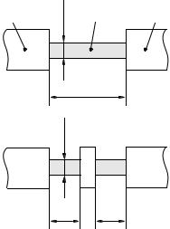
The flicker noise in a thin-film resistor measured under a dc current through the sample is determined by noise in the resistive film and noise in the contacts. To separate noises of the contacts and resistive film, we used special test structures shown in Fig. 2. The samples of resistive structures (a) and (b) are situated on the same substrate and differ in the ratio of resistive-film length to its width (the number of squares) and have different number of contacts.
Denote by S1 and S2 the power spectral densities of noise in the resistive structures shown in Figs. 2a and 2b, respectively; Sc is the power spectral density of a single contact of the resistive structure under a constant current density through the contact and the constant width of the structure (b = const); N1 and N2 are the numbers of contacts in structures (a) and (b), respectively; Ssq1 is the power spectral density of noise in a single square of the resistive film when the current density is the same in structures (a) and (b); n1 and n2 are the numbers of squares of the resistive film in structures (a) and (b), respectively; and t1 and t2 are the ratios of the number of contacts to the number of squares in structures (a) and (b), respectively (t1 = N1/n1 and t2 = N2/n2).
JOURNAL OF COMMUNICATIONS TECHNOLOGY AND ELECTRONICS Vol. 44 No. 2 1999
208 |
ZHIGAL’SKII, KAREV |
(a) |
b |
|
|
|
Cu |
Ta x Ny |
Cu |
||
|
|
a1 |
(b) |
|
b |
|
a2 |
a2 |
Fig. 2. Design of the test samples of resistive structures for separating the noise in contacts for b = 100 m; (a) a1 =
2500 m, the number of contacts N1 = 2, the number of squares in the film is n1 = a1/b = 25, and t1 = N1/n1 = 0.08;
(b) a2 = 500 m, the number of contacts N2 = 4, the number of squares in the film is n2 = 2a2/b = 10, and t2 = N2/n2 = 0.4.
Assuming that there is no correlation between the excess noise in the resistive film and in contacts, we obtain the system of equations
S1 = N1Sc + n1Ssq1
S2 = N2Sc + n2Ssq1.
Solving this system for Sc and Ssq1 , we obtain the expressions for the power spectral densities of noise in a single contact,
n1 S2 – n2 S1
Sc = ----------------------------, n1 n2 (t2 – t1 )
and in a unit square of the resistive film,
N1 S2 – N2 S1
S = -----------------------------.
sq1 n1 n2 (t1 – t2 )
Investigations directed to the identification of the contribution of noises in contacts and in the resistive layer to the total flicker noise in the resistor are carried out on thin-film resistors manufactured by industrial
Power spectral density of noise in the contacts of the Ta-film- based resistive structures
Group |
1 |
2 |
3 |
4 |
|
|
|
|
|
Sc × 1016, V2/Hz |
3500 |
– |
4 |
0.32 |
|
|
|
|
|
microwave large-scale integrated-circuit technology on the basis of tantalum films [6].
The resistive films were deposited on glass-ceramic substrates by the magnetron sputtering from a tantalum target in the argon–nitrogen gas mixture (with 10% of nitrogen) at various deposition rates. The deposition rate was controlled by the voltage applied to the target by varying the target current It . The pressure of the gas
mixture was maintained at a level of (7–10) × 10–2 Pa during all processes. The geometric dimensions of a sample were chosen as follows (see Fig. 2): the length a1 = 2500 µm and a2 = 500 µm; the width b = 100 µm. The surface resistivity of the film in all the samples under investigation was equal to 100 ± 10 Ω / . The contacts to the resistive layer were fabricated on the basis of a copper film with a chromium sublayer by the vacuum thermal sputtering under the residual-gas pressure at most 7 × 10⁻⁴ Pa. After that, copper, nickel, and gold layers of the thickness hCu = 5 µm, hNi = 0.5 µm, and hAu = 2 µm, respectively, were successively deposited by the electrodeposition technology.
We investigated the resistor samples of four groups that differ by the conditions under which the resistive layer was deposited and the contacts were fabricated. The first and second groups differ by the deposition rate of the resistive layer. In the first group, the deposition was performed under the target current It = 1.5 A (high deposition rate), whereas, in the second, the deposition was performed under It = 0.3 A (low deposition rate).
In the samples of the third and fourth groups, the resistive film was deposited under identical conditions that are chosen to provide the minimum noise level. In the third group, the contacts were deposited after preliminary depressurization of the vacuum chamber, whereas, in the fourth group, the resistive layers and the contacts were fabricated in a single technological procedure, without depressurizing the chamber.
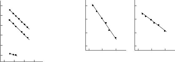
Figure 3 represents the power spectral density of the 1/f noise in TaxNy films as a function of frequency for the resistive structures; the power spectral density of the 1/f noise in the contacts, Sc, measured at the frequency f = 130 Hz under the dc current I0 = 6 mA is shown in the table.
Figure 2 and the table clearly show that the structures of the first group, which are obtained at the highest deposition rate, are characterized by the maximum level of the 1/f noise. The resistive layer in these structures has a low content of nitrogen, which results in intense oxidization during subsequent annealing and, as a consequence, leads to high-level noise in the contacts, which becomes comparable with the noise in the resistive film.
Unlike the structures of the first group, the structures of the second group, which were deposited at a low rate, are characterized by a substantially higher content of nitrogen. In this case, the oxidization processes under the thermal treatment are substantially
JOURNAL OF COMMUNICATIONS TECHNOLOGY AND ELECTRONICS Vol. 44 No. 2 1999
NONEQUILIBRIUM FLICKER NOISE IN TANTALUM-BASED THIN-FILM RESISTORS |
209 |
||||||||
Ssq × |
1016, V2/ Hz |
S × |
1016, Hz –1 |
|
S × 1012, Hz –1 |
|
|||
105 |
|
103 |
|
(a) |
|
103 |
|
(b) |
|
104 |
|
102 |
|
|
|
102 |
|
|
|
|
|
|
|
|
|
|
|
||
103 |
|
1 |
|
|
|
|
|
|
|
102 |
2 |
101 |
|
|
|
101 |
|
|
|
|
|
|
|
|
|
|
|||
101 |
|
100 |
|
|
|
100 |
|
|
|
10 |
0 |
3 |
|
101 |
102 |
103 |
101 |
102 |
103 |
|
|
|
|
f, Hz |
|
|
f, Hz |
||
|
|
|
|
|
|
|
|||
|
|
101 102 103 |
104 f, Hz |
|
|
|
|
|
|
Fig. 3. The power spectral density of the 1/f noise in tanta- lum-based resistive films as a function of frequency; (1) samples of the first, (2), second, and (3), third and fourth groups.
Fig. 4. The relative power spectral density of the 1/f noise as a function of frequency for the resistors from the second group (a) for measurements under a dc current and (b) for measurements of the dc voltage component under pulse influence.
suppressed. This results in a decrease in the 1/f noise in contacts, which cannot be singled out due to a relatively high level of noise in the resistive film.
The results obtained by measuring the power spectral density of the contact noise in the samples of the fourth group (in which the contact noise is by an order of magnitude lower than that in the samples of the third group) confirm the fact that the contact noise is attributed, first of all, to the gas adsorption followed by the oxidization of the resistive-film surface. The minimum level of the contact noise observed in the samples of the fourth group is explained by the absence of the oxidized layer in the contact region.
Thus, depending on the manufacturing technology, the contribution of the contact noise to the flicker noise of a resistor under dc current measurements can be comparable to or exceed the noise of the resistive film. A significant contribution of the contacts to the total noise level of the resistor may be associated with the nonmetal character of the conductivity in the vicinity of a contact. In high-quality thin-film resistors, the 1/f noise due to the contacts is negligible.
Using the software developed, we determined coefficients bn in power series (2) and parameters Z and β in the power approximation of the VCC for the set of samples available.
Practically, the power approximation (3) proves to be more effective and expedient. For example, the above parameters for the samples of the first group are as follows: β 2.64 and Z –43.1 Ä1 – β .
We investigated the nonequilibrium 1/f noise in the samples of the second technological group, in which the measurements performed under a dc current with the test structures shown in Fig. 2 did not allow us to single out the flicker noise of the contacts. We compared the 1/f noise measured under a pulse voltage
applied to the sample with the flicker noise measured under a dc current and the dc voltage U0 = RI0 across the sample that is equal to the amplitude of the pulse voltage Up = 5 V.
The spectral densities of fluctuations of the dc voltage component depend on frequency as 1/f with the exponent γ = 0.7–0.9, whereas this exponent is γ = 1−1.2 for the flicker noise measured under a dc current. The noise levels in these two cases also are different. For example, the power spectral density of the 1/f noise measured in a thin-film resistor at a frequency of 10 Hz under a dc current (under the voltage U0 = 5 V across a sample) exceeds the power spectral density measured under a pulse voltage of the amplitude Up = 5 V by more than three orders of magnitude. This result shows that the contribution of nonequilibrium conductivity fluctuations to the total flicker noise measured under a dc current with U0 < 5 V is negligible.
At the same time, the relative spectral density of fluctuations of the dc voltage component is greater than the relative spectral density of the flicker noise S = SU/U2 by three orders of magnitude (at the frequency 10 Hz; see Fig. 4), which indicates that the noise amplitude of the dc voltage component is strongly modulated. The basic contribution to the dc voltage component and, hence, its fluctuations, is due to the contacts of the resistive film.
Note that a thin-film resistor is maintained under different temperature conditions during the measurements under a dc and pulse currents. Calculations show that a resistor may be overheated under the dc measurements due to the Joule heat to the temperatures that are by 30–50 K higher as compared with the measurements under pulse conditions. To determine the effect of temperature on the noise level under a pulse influence and a given dc current through the sample, we measured
JOURNAL OF COMMUNICATIONS TECHNOLOGY AND ELECTRONICS Vol. 44 No. 2 1999
210 |
ZHIGAL’SKII, KAREV |
the power spectral density of noise in the temperature range from 300 to 400 K for U0 = Up = 5 V [7]. As the temperature increases, the flicker-noise level increases, and the level of fluctuations of the dc voltage component decrease. The latter fact is associated with a decrease in the resistance of the thin-film contacts as the temperature increases. An increase in the flickernoise level with temperature under dc-current measurements is attributed to the activation of mobile lattice defects (vacancies) in the conducting film [8, 9].
CONCLUSION
The results obtained allow us to conclude that the mechanisms of the flicker noise observed under a dc current through a sample and under fluctuations of the dc voltage component generated by a series of rectangular current pulses have different physical natures. For a comparatively low dc current density through the sample (j < 105 A/cm2), the flicker noise is determined by the equilibrium fluctuations of the term R0 in (1). The fluctuations of the dc voltage component are related to the nonequilibrium conductivity fluctuations of the nonlinear component of the VCC by expression (9).
The method described for investigating the 1/f noise can be used for the analysis of nonequilibrium fluctuations in various types of passive two-terminal devices
characterized by weak nonlinearity and can find applications in nondestructive testing in the fabrication of integrated circuits to assess the quality of contacts, interlayer junctions, etc.
REFERENCES
1.Hooge, F.N., Kleinpenning, T.G.M., and Vandamme, L.K.J., Rep. Prog. Phys., 1981, vol. 44, no. 5, p. 479.
2.Weissman, M.B., Rev. Modern Phys., 1988, vol. 60, no. 2, p. 537.
3.Jones, B.K., Electron. Lett., 1976, vol. 12, no. 4, p. 110.
4.Zhigal’skii, G.P., Abstracts of Papers, 7th Vilnius Conf. on Fluctuation Phenomena in Physical Systems, Palanga, 1994, p. 285.
5.Potemkin, V.V., Stepanov, A.V., and Zhigal’skii, G.P., Abstracts of Papers, AIP Conf. on Physical Systems and 1/f Fluctuations, St. Louis, 1993, p. 61.
6.Zhigal’skii, G.P., Karev, A.V., and Kosenko, V.E., Elektron. Tekh., Ser. 6: Materialy, 1992, no. 1(148), p. 70.
7.Zhigal’skii, G.P. and Karev, A.V., Abstracts of Papers,
13th Int. Conf. Noise in Physical Systems and 1/f Fluctuations, Singapore: World Scientific, 1995, p. 323.
8.Zhigal’skii, G.P., Pis’ma Zh. Eksp. Teor. Fiz., 1991, vol. 54, no. 9, p. 510.
9.Zhigal’skii, G.P., Usp. Fiz. Nauk, 1997, vol. 167, no. 6, p. 623.
JOURNAL OF COMMUNICATIONS TECHNOLOGY AND ELECTRONICS Vol. 44 No. 2 1999