

ЛЕКЦИИ ФШФС_2007 / НАШИ СТАТЬИ / JCTE1301_MOS 1999
.pdfJournal of Communications Technology and Electronics, Vol. 44, No. 12, 1999, pp. 1301–1317. Translated from Radiotekhnika i Elektronika, Vol. 44, No. 12, 1999, pp. 1413–1430. Original Russian Text Copyright © 1999 by Zhigal’skii.
English Translation Copyright © 1999 by åÄàä “ç‡Û͇ /Interperiodica” (Russia).
REVIEW
Excess Noise in Metal–Dielectric–Semiconductor Structures
G. P. Zhigal’skii
Received April 6, 1999
Abstract—Excess noise in metal–dielectric–semiconductor (MDS) capacitors is investigated in the cases when the device contains either planar or relief dielectric used as an insulation of the elements in modern microcircuits. The nature of the noise initiated in the structures with high and negligible leakage currents as well as in the structures with thin (the layer thickness is about 10–100 nm) and ultrathin (2–5 nm) dielectric is studied. The influence of the material of the gate on the excess noise is revealed. The excess noise in the considered structures can be caused by physical processes on the dielectric–semiconductor and metal–dielectric phase interfaces, the mechanisms of the dielectric current flow, and the generation–recombination (GR) processes in the space-charge region (SCR) of the semiconductor. The influence of the γ -radiation treatment of the MDS structures on the excess noise level is investigated in different operation modes. The obtained results show that the excess noise is a sensitive diagnostic tool for the quality of the MDS structure.
INTRODUCTION
The excess noise in the insulated-gate field-effect [metal–dielectric–semiconductor (MDS) or metal– oxide-semiconductor (MOS)] transistors (FETs) have been extensively studied since the 1960s [1–6]. However, the publications on the excess noise (the noise whose level exceeds the level of the thermal noise) of the MDS capacitors are still limited in spite of the fact that the MDS capacitor is a simpler structure than the MDS transistor. Using the MDS capacitor one can investigate the excess noise in different operation modes (the surface depletion, enhancement, and inversion modes) [7] and in the presence of high-intensity electric fields, while, in the induced-channel MDS transistor, the excess noise can be measured only in the mode of strong inversion.
The excess noise in the MDS capacitors with the thickness of the dielectric layer hox = 10–100 nm is thoroughly investigated in [8–18], where the noise is studied in different operation modes including the case when the gate voltages approaches the level that causes the dielectric breakdown. In recent years, the design of MOS integrated microcircuits (IMs) has been oriented toward decreasing the thickness of the gate dielectric up to hox = 2–10 nm. This tendency is reflected in a number of papers on the noise in the MDS structures with the ultrathin dielectric layer [19–22].
The purpose of this survey is to generalize the results of experimental investigations of the excess noise in the MDS capacitors with dielectric of different types which were obtained by the author and other researches during the last two decades. Among various forms of the excess noise, the generation–recombina- tion (GR) noise, the 1/fγ noise (the flicker noise), and the noise in the form of random telegraph signals (RTSs) are considered. In this paper, the 1/f noise is studied in most detail. The excess noise generated in
the unbiased structure under the quasi-equilibrium conditions, which was investigated in [13, 14, 16], is not addressed in this survey.
PHYSICAL MODELS OF THE MECHANISM OF THE 1/f NOISE
IN THE MDS STRUCTURES
A number of models are suggested to explain the 1/f noise in the MDS transistors. Among them, the following two alternative approaches are referred to as the basic models.
(1) The model of the dielectric–semiconductor electron interaction [1–4] based on Mc Whorter’s ideas [23]. According to this model, it is assumed that the noise is initiated by the fluctuations of the charge-car- rier concentration in the channel, which are caused by random carrier trapping and detrapping in the oxide near the Si–SiO2 interface. These fluctuations modulate not only the number of free carriers in the channel but also the semiconductor surface voltage and, hence, the gate voltage. A mathematical form of the 1/f spectrum is obtained by choosing the appropriate distribution of the lifetime of the carriers trapped in the oxide during tunneling transitions. This model is commonly called the trapping or surface model.
(2) The three-dimensional model, according to which the 1/f noise is caused not by surface but by bulk phenomena, namely, fluctuations of the charge-carrier mobility in the channel due to the carrier scattering by acoustic phonons. Vandamme developed this model for the MDS transistors in 1980 [24, 25] on the basis of Hooge’s concepts [26, 27]. In this model, the existence of the 1/f spectrum is postulated. In addition, it is assumed that all scattering mechanisms that are different from the lattice mechanism decrease the 1/f noise.
1301

1302
(a)
Me (probe)
Me (gate)
 SiO2, Ta2O5
Si
ZHIGAL’SKII
inversion modes. In the MDS capacitor with the ultrathin SiO2 layer, the conductivity is provided by the carrier tunneling through the oxide. In thicker layers, the carriers can be transported through the dielectric by the Poole–Frenkel or Schottky emission [7].
(b) Et
Nt(Et)
SiO2
(c)Et
Nt(Et)
SiO2
Al (lower gate)
Ec
Ei
F
 Ev
Ev
Si
Ec
Ei
F
Ev
Si
Fig. 1. (a) The MDS structure and the semiconductor Fermi levels in the (b) depletion and (c) inversion modes; Nt(Et)
the distribution of the oxide trap energy density.
In a number of papers [28, 29, 6], it is found that some of the MDS devices tested for the presence of noise are better described by the trapping, while other devices are better described by the three-dimensional model. Therefore, later, the 1/f noise models were developed which simultaneously took into account the fluctuations of the carrier number and mobility in the channel [3, 5, 30, 31].
In the MDS capacitor shown in Fig. 1, the current on the dielectric–semiconductor interface is absent during the measurements of the gate voltage fluctuations. Therefore, the mechanism of the 1/f noise in the channel due to the carrier scattering by phonons cannot be described in terms of the three-dimensional model. At the same time, the excess noise in the MDS capacitors can be caused by the physical processes on the dielec- tric–semiconductor and metal–dielectric phase interfaces, mechanisms of the dielectric current flow, and the GR processes in the semiconductor space-charge region (SCR). These processes manifest themselves when the MDS capacitor operates in the depletion and
Consider the trap model of the 1/f noise as applied to MDS structures. It is assumed that, in the MDS transistor or capacitor, the surface electron trapping– detrapping process occurs in two stages [32]. At first, the carriers are trapped by the fast semiconductor– dielectric interface states (ISs) with the energy corresponding to the bandgap of the semiconductor, and, then, they tunnel to the oxide traps, which have approximately the same energy level. The existence of fast ISs is due to the presence of the excess silicon or impurity atoms. Their density depends on the crystal orientation [7]. The fast ISs are characterized by the small relaxation times and continuous U-shaped energy distribution over the bandgap, which increases in density towards the boundary of the band [7]. Therefore, the 1/f spectrum at low frequencies cannot be attributed to the fast IS recharging.
Long relaxation times are due to the carrier tunneling from fast ISs to the oxide traps, which are spatially distributed in the dielectric volume and have the energy level within the semiconductor bandgap. The relaxation time of the carrier tunnel transition exponentially depends on the distance between the oxide trap location and the Si–SiO2 interface. This time is specified by the formula [1–4]
τ (z) |
2z(2m*W )1/2 |
, |
(1) |
= τ s exp -------------------------------- |
|||
|
|
|
|
where τ s is the time constant of the fast ISs on the Si– SiO2 interface corresponding to z = 0, z is the distance from the interface to the oxide trap location, m* is the effective electron mass, W is the barrier height on the interface, and is the Planck constant divided by 2π . It is commonly accepted that τ s = 10–10–10–8 s [1, 3]. For the potential barrier of the height W = 4 eV and m* = m0 (m0 is the electron rest mass), (1) implies [1, 3]
τ (z) = τ s exp (λ T z), |
(2) |
where λ T = 2 × 108 cm–1 is the SiO2 tunneling parameter. A wide range of time constants τ (z) can be provided when the traps are distributed throughout the oxide thickness. Thus, when z varies from 0 to 2 nm, according to (2), τ varies by a factor of 1017 and reaches the value 2 × 10⁸ s at z = 2 nm.
A single trap level with relaxation time τ provides the Lorentz spectrum of fluctuations of the number of the filled traps; hence, the density of the carriers trapped from the surface channel (∆ N is the number of
JOURNAL OF COMMUNICATIONS TECHNOLOGY AND ELECTRONICS Vol. 44 No. 12 1999
EXCESS NOISE IN METAL–DIELECTRIC–SEMICONDUCTOR STRUCTURES |
1303 |
these carriers) on the element of the gate area ∆ x∆ y in the energy interval ∆ Et is expressed by the formula [1, 4]
S∆ N ( f ) |
τ∆ x∆ |
|
y∆ |
Et |
, |
(3) |
= 4 Nt (Et, z) f t (1 – f t )------------------------- |
||||||
|
1 + |
ω |
2 |
τ 2 |
|
|
where Nt(Et, z) is the energy density (measured in J–1 m–2) of the slow oxide traps considered with respect to energy Et and coordinate z and ft is the Fermi–Dirac function
f t = |
nt |
|
1 |
----- = |
---------------------------------------------- . |
||
|
Nt |
1 |
+ exp (Et – F)/kT |
Here, nt is the density of filled traps, F is the Fermi energy (quasi-level), k is the Boltzmann constant, and T is the absolute temperature.
In (3), the product ft(1 – ft) has a sharp maximum at Et = F and steeply decreases as energy Et deviates from Fermi energy F. Hence, this product is finite only in the range of energies about kT in the vicinity of F. Therefore, only the traps located near the Fermi level contribute to spectrum (3) of the carrier density fluctuations. When the oxide traps are uniformly distributed in the depth interval (0, z1) (depth z is measured from the Si– SiO2 interface), i.e., Nt is characterized by a uniform behavior, the corresponding time constants τ 1 and τ s are determined from (2). In this case, normalized distribution function g(τ ) is expressed as [33]
|
|
dτ /τ |
for τ s < τ <τ 1 , |
g(τ )dτ |
|
----------------------- |
|
= |
ln (τ 1 /τ s )1 |
|
|
|
|
0 for τ >τ |
1 . |
|
|
Here, τ 1 corresponds to the maximum depth of the oxide trap location, whereas, according to (2), τ s is the minimum relaxation time. Integrating expression (3) weighted with g(τ ) with respect to Et, x, and y yields the 1/f spectrum for the fluctuations of the number of carriers trapped in the MDS transistor channel [4]
SN = |
Nt (F)kTWL |
= |
Nt (F)kTWL |
(4) |
----------------------------- |
-----------------------------. |
|||
|
f ln (τ 1 /τ s ) |
|
λ T z1 f |
|
Here, Nt(F) is the effective energy density of the slow oxide traps at the trap energy level Et which is equal to Fermi energy F throughout the depth interval (0, z1), Nt(F)kT is the density (measured in m–2) of the oxide traps in the vicinity of the Fermi level, and W and L are, respectively, the width and length of the MOS transistor channel.
Expression (4) holds in the case of the homogeneous MDS transistor channel, i.e., when the drain voltage is equal to zero relative to the source voltage. This expression can be used for the MDS capacitor with the gate area Ag = WL in both the enhancement and inversion modes. The spectral density (SD) of the charge (Qox) fluctuations on the Si–SiO2 interface is SQ = e2SN,
where e is the electron charge. The SD of the fluctuations of the flat band and gate voltages (UFB and U, respectively) is coupled with SD SQ of the charge fluctuations via capacitance Cx of the MDS capacitor [4]. Taking into account (4), SU(f) can be expressed in the form
SU ( f ) = |
SQ |
= |
e2 |
Nt (F)kT |
, |
(5) |
C-----------2x Ag2 |
C2x Ag2 |
λ T z1 f |
||||
|
|
|
----------- |
-------------------- |
|
|
where Cx is the capacitance of the MDS capacitor per unit area measured in F/m2 .
It is known [7] that for the idealized MDS structure operating in the surface-depletion mode, Cx is the capacitance of two series capacitors. Capacitance Ci of one of them is due to the presence of the dielectric layer and equals Ci = ε 0ε /hox, where ε 0 is the permittivity of vacuum and ε is the relative permittivity of the oxide. This capacitance is independent of the structure voltage. Capacitance Cd of the other capacitor is due to the existence of the semiconductor SCR, and equals Cd = ε 0ε 1/d [7], where d is the width of the semiconductor SCR depending on gate voltage U and ε 1 is the permittivity of the semiconductor. In the enhancement mode, capacitance Cx in (5) equals the oxide capacitance per unit area, i.e.,
Cx = Cx0 = Ci = ε 0 ε /hox . |
(6) |
In (5), SD SU of the 1/f noise power depends on the gate voltage because the position of the Fermi quasilevel in the dielectric varies with the gate voltage and is governed by the energy density of the traps Nt(F), which coincides with Fermi level F. In addition, capacitance Cx of the MDS capacitor per unit area involved in (5) varies with the gate voltage.
Generally speaking, the dielectric traps may be nonuniformly distributed along the z coordinate and over energy Et within the bandgap [1]. Figure 1 illustrates the case of a nonuniform distribution of the dielectric trap energy density and shows the position of the Fermi level of the p-type semiconductor operating in the depletion and inversion modes. Here, Ec, Ei, and Ev are the energies of the bottom of the conduction band, middle of the bandgap, and top of the valence band, respectively. One can see from this figure that trap efficiency Nt(F) varies with gate voltage U.
For the enhancement mode, at T = 300 K, one can represent (5) in the form
SU ( f ) = |
8.9 |
× 10–38 Nt (F)hox2 |
, |
(7) |
|
------------------------- |
--------------------- |
||||
|
|
Ag |
λ T z1 f |
|
|
taking into account (6) and substituting constants e, k, ε 0, and ε = 3.9 [7].
JOURNAL OF COMMUNICATIONS TECHNOLOGY AND ELECTRONICS Vol. 44 No. 12 1999
1304 |
ZHIGAL’SKII |
NOISE IN THE MDS STRUCTURES WITH THIN AND ULTRATHIN PLANAR DIELECTRIC LAYERS
Test Structures and Experimental Technique
The test structures investigated in [8–18] are fabricated on the plates of the boron-doped silicon (KDB-0.5, KDB-4.5, KDB-7.5, KDB-10, KDB-12) with the p-type conductivity and crystallographic orientation (100) and on the plates of the phosphorusdoped silicon (KEF-4.5, KEF-10) with the n-type conductivity. The examined MDS structures are manufactured with the help of different technologies using the SiO2 (MOS structures), Ta2O5 , and two-layer SiO2– Si3N4 (metal–nitride–oxide–semiconductor (MNOS) structures) dielectrics. A single plate is used for the structures with the gate areas Ag = 0.2–1 mm2 [8–11, 15].
Silicon dioxide 30–100-nm layers were obtained by oxidizing thermally the plates in the atmosphere of dry oxygen with the gas hydrogen chloride additive (1.5−3% volume) at the temperature T = 1300K. The oxidation of the silicon plates was preceded by the standard chemical cleaning (CC) or plasmachemical treatment (PCT). Sometimes, the combined treatment was applied. At first, the plates were plasmachemically treated and then, chemically cleaned. Structures with different electrophysical properties were obtained by varying the technological conditions [11, 15]. Silicon oxide films in the structures with thin (hox = 10–30 nm) dielectric were obtained at relatively low oxidation temperatures (less than 1150K) [17, 18]. The interest in these structures is due to the fact that IMs based on the MOS transistors with the channel shorter than 1 µm are fabricated using a thinner gate dielectric. For these structures, dielectric layers were obtained by thermal or pyrogenic oxidation and by plasmachemical oxinitride deposition [34]. Tantalic pentoxide films were fabricated by decomposing tantalum pentaethylate in the glow-discharge plasma [11].
The gates were manufactured of aluminum, molybdenum, or polysilicon Si*. After deposition, the polysilicon film was doped with phosphorus or boron to obtain the surface resistance equal to 20 Ω / . Then, the plates were annealed in the nitrogen atmosphere at 1273K. The Al and Mo films were 1 µm thick and the polysilicon films were 560 nm thick. The Al and Mo films were fabricated by electron-beam evaporation and ion sputtering, respectively. The gates were photolithographed by the standard technology.
To provide an ohmic contact with the bulk semiconductor region, the Al 1-µm layer was deposited by the thermal evaporation in vacuum on the back surface of the plate and then, annealed in the argon atmosphere at 600–775K. Before aluminum was deposited, the oxide had been etched away from the plate surface. As many as 500 structures were implemented on each plate. A laser ellipsometer controlled the dielectric thickness. Figure 1a displays the MDS structure described above.
The SD of the noise power was measured in the band 2 Hz–200 kHz. Storage batteries supplied the dc bias voltage in the range U = 0–10 V via the 5.7-MΩ resistor. The noise generated by the bias supply circuit was determined using the bridge circuit [35, 11]. The intrinsic noise of the preamplifier was measured when the MDS structure was replaced by the air-dielectric capacitor with the capacitance equal to the capacitance of the structure or by the equivalent RC circuit. The preamplifier was based on the KP-303A FETs. Its input resistance was 10 MΩ . The level of the intrinsic noise of the measuring facility did not exceed 10–28– 10−29 A2/Hz in the band 20 Hz–20 kHz. In addition to the excess noise, dielectric leakage current I was measured with electrometers.
The thermal noise of the MDS capacitor was calculated by the Nyquist formula using the measurements
of the dielectric dissipation factor tan δ at different frequencies [36] or determined by measuring the SD of the noise power when the MDS structure was replaced by the equivalent RC circuit [10]. When processing the experimental results, the thermal noise of the MDS capacitor was subtracted from the total measured noise power.
The effective dielectric charge per unit area Qox was determined using the method of hf voltage–capacitance characteristics (VCCs) (the C–V method) [7]. The measurements were performed at 0.3–1 MHz. The effective dielectric charge was determined by voltage shift UFB of the flat bands of the experimental VCC with respect to the calculated VCC. The value of the mobile charge in the oxide was determined by thermal–field tests performed during 20–50 min at the electric field intensity in the dielectric ~(1–6) MV/cm and T = 470–500K.
Density D of the fast ISs was found using the Gray– Brown temperature method [37], which is based on the effect of the IS charge variation caused by the variation of the position of the Fermi level in the semiconductor. The density of the fast ISs can be determined by voltage shift ∆ UFB of the flat bands from the VCC measurements under the standard conditions (T = 295K) and at the liquid nitrogen temperature (T = 77K) [7].
The Excess Noise of the MDS Structures Operating
in Different Modes
The excess noise was investigated in the MOS structures with the oxide 10–100-nm layers and 0.2–1-mm2 gates. The structures with low (I < 25 pA) and high (I > 0.1 µA) leakage currents (observed at the electric field intensity in the dielectric Eox = 8 MV/cm) were examined experimentally [10, 15]. The excess noise was studied when the state of the semiconductor surface varied from the enhancement mode to the strong inversion.
Different structures implemented even on the same plate exhibit individual features in the behavior of the
JOURNAL OF COMMUNICATIONS TECHNOLOGY AND ELECTRONICS Vol. 44 No. 12 1999
EXCESS NOISE IN METAL–DIELECTRIC–SEMICONDUCTOR STRUCTURES |
1305 |
SDs of the MOS capacitor noise power measured versus bias gate voltage U. This effect is caused by different distributions of the oxide traps over energy Et and along the z coordinate and the presence of the dielectric leakage currents. The analysis of the SDs of the noise power measured versus the gate bias voltage for a great number of MOS capacitors implemented in various technologies revealed the mechanisms of processes in these structures [8, 10, 15, 17].
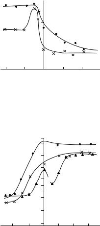
Figures 2 and 3 display the typical SDs of the excess noise power of the MOS capacitors with low leakage currents implemented on the substrates with the n- and p-type conductivity measured versus the bias voltage [17, 18].
For certain structures, the behavior of SU(U) is characterized by humps (curves 2 in Fig. 2 and 3 in Fig. 3). The analysis of VCCs of these structures shows that the hump location on the voltage axis corresponds to the weak-inversion mode. The structures implemented on the KDB-4.5 plates (hox = 50 nm) exhibit the existence of a maximum in S(U) when operating in the depletion mode [10]. The location of this maximum on the voltage axis is preserved in the temperature range 295−450 K although the noise level increases with the temperature increasing up to 350 K, after which it decreases with the increasing temperature. For other structures, the noise level increases as the structure is cooled to 77 K [16]. These results can be explained using the trapping model of the excess noise. Within the framework of this model, the maximum location on the voltage axis (curves 2 in Fig. 2 and 3 in Fig. 3) is governed by the depth (measured along z) of the trap occurrence and the oxide trap energy level.
It is known [7] that when silicon is thermally oxidized, the traps are formed in the oxide and on the oxide–silicon interface. The distribution of the traps Nt(E) over energy is nonuniform and usually has a maximum in the vicinity of the silicon midgap. Following the shift of the semiconductor permitted-band boundaries on the Si–SiO2 interface, the position of the trap energy levels varies with respect to the Fermi level with the gate voltage [7] (Figs. 1b, 1c), which results in the change of the trap efficiency. Since the maximum contribution to the excess noise is due to the traps with the energy levels approaching the Fermi energy according to (5), the location of the maximum observed on the graphs of SU(U) can be explained taking into account the position of the maximum in the energy distribution Nt(Et) of the traps with respect to the silicon midgap. Namely, at a certain bias voltage on the MDS structure, the existence of the bend of energy bands on the Si– SiO2 interface causes the coincidence of the maximum trap density in distribution Nt(Et) with Fermi energy F, which explains the occurrence of the maximum on the graph of the SD of the noise power versus the bias voltage. I assume that the occurrence of the maximum is caused by the monoenergetic traps located at the depth z0 measured from the Si–SiO2 interface. Since only
SU × 1017, V2 Hz– 1
101
|
1 |
|
|
|
2 |
|
|
|
100 |
|
|
– 2 – 1 |
0 |
1 |
2 U, V |
Fig. 2. SDs of the excess noise power of the MOS capacitors with the Al gate implemented on the KEF-4.5 n-type silicon
vs. the bias voltage at f = 65 Hz and Ag = 0.25 mm2; hox = (1) 20 and (2) 11 nm.
SU × 1017, V2 Hz– 1 |
|
102 |
1 |
|
|
2 |
|
3 |
|
101 |
|
100
– 2 – 1 0 1 2 3
U, V
Fig. 3. SDs of the excess noise power of the MOS capacitors implemented on the p-type silicon vs. the bias voltage for the structures on (1) KDB-7.5 and (2) and (3) KDB-0.5 sub-
strates at f = 110 Hz and Ag = 0.61 mm2; (1) Al gate, hox = 12 nm and D = 7.7 × 1011 cm–2; (2) Al gate, hox = 20. 8 nm and D = 5.6 × 1011 cm–2; and (3) Mo gate, hox = 20.9 nm and D = 4.4 × 1011 cm–2.
the traps located in the vicinity of the Fermi level in the interval of energies about kT contribute to the carrier density fluctuation spectrum, one can assume that the energy width of the peak observed in SU(U) is kT. Then, when the oxide voltage drop varies within the peak width ∆ U, the Fermi level scans the trap level in the interval of energies about kT, and the depth of occurrence of the trap centers is specified by the formula
z0 = kT hox e∆ Uox , |
(8) |
where ∆ Uox is the oxide voltage drop observed when the MDS structure voltage changes by ∆ U.
Using formula (8), the depth z0 (measured along the z coordinate) of occurrence of the trap level is estimated
JOURNAL OF COMMUNICATIONS TECHNOLOGY AND ELECTRONICS Vol. 44 No. 12 1999
1306 |
ZHIGAL’SKII |
in [18] for the MOS capacitor and the value z0 = 1.5 nm is obtained. Function SU(U) for this capacitor is plotted in Fig. 3 (curve 3). For the structure characterized by function SU(U) presented in Fig. 2 (curve 2), z0 = 1.7 nm. The calculated values of z0 agree with the known results [1] on the location of the oxide traps obtained for the MDS transistors by other methods.
In [18], the SD of the MOS capacitor noise power is quantitatively estimated; corresponding function SU(U) is plotted in Fig. 3 (curve 3). In calculations, the trap distribution over energy is assumed to be uniform in the semiconductor gap band. The effective oxide charge in this structure is determined from the VCC [7] and equals Qox = 5 × 10⁻⁴ C m–2. The energy density of the traps is specified through the oxide charge as Nt =
Qox /e∆ Eg = 1.8 × 10⁻³³ m–2 J–1, where ∆ Eg = 1.11 eV is the width of the silicon bandgap. The substitution of Nt ,
hox = 20.5 × 10⁻⁹ m, Ag = 0.61 × 10⁻⁶ m2 , z1 = z0 = 1.5 × 10⁻⁹ m, λ T = 2 × 10¹⁰ m–1, and f = 110 Hz; and Cx
into (7) yields SU = 3.4 × 10⁻¹⁷ V2 Hz–1 for the surface enhancement mode; taking into account Cx involved in (5), one obtains SU = 7 × 10–16 V2 Hz-1 for the inversion mode. The calculations fit the experimental data, which is supported by the trapping model of the mechanism of the 1/f noise in the investigated MDS capacitors. One should keep in mind that, in the inversion mode, the oxide traps interact with the minority (with respect to the substrate) carriers, for which the trap density may differ from the trap density for the majority carriers in the depletion mode.
One can see from Figs. 2 and 3 that the SD of the excess noise power of the MDS structures operating in the enhancement and strong inversion modes does not depend on gate bias voltage U. This fact is consistent with formula (5) because, when the traps are uniformly distributed over energy, their energy density Nt(F) do not depend on the gate voltage, as well as capacitance Cx in the enhancement and strong inversion modes. For the MDS structures (based on silicon with the p- or n-type conductivity) with low leakage currents, the SD of the noise power observed in the inversion mode is 1−3 orders of magnitude greater than in the enhancement mode. In fact, in the inversion mode, the SCR is formed in the semiconductor, and the capacitance of the MDS structure appears to be smaller than in the enhancement mode. Therefore, according to (5), function SU(U) is greater in the inversion mode than in the enhancement mode.
At the same time, it is found that the MDS structures with the high density of structure defects in the vicinity of the Si–SiO2 interface and in the SCR of the semiconductor exhibit a higher-level excess noise than that predicted by the trapping model. This is due to the fact that, for these structures operating in the inversion mode, the SCR GR processes contribute to the excess noise, and the noise spectrum observed in this case is
the sum of the 1/f and GR noises. Similar structures are investigated in [10, 15]. However, the structures examined in this paper (the corresponding results are presented in Figs. 2 and 3), have a low density of the structure defects in the vicinity of the Si–SiO2 interface and in the SCR of the semiconductor. According to the experimental results, the rate of the GR processes in these structures is low (when the nonequilibrium VCC was measured, the transient time of the formation of the inversion layer was as long as several hundreds seconds). Therefore, the SCR GR noise is not observed, and these structures exhibit a good agreement between the results provided by the trapping model and experimental data both in the surface enhancement and inversion modes.
Comparing the experimental data on the 1/f noise level observed in the inversion mode for the MOS structures based on the p-type silicon and the data for the structures of equivalent sizes based on the n-type silicon, one can see that the latter structures are characterized by the noise whose level is higher by a factor of 10–15. This result agree with the investigations of MDS transistor noise, according to which the level of the 1/f noise in the n-channel transistors is 5–15 times higher than that in the p-channel transistors [6, 38]. The reason is that, when carriers tunnel to the oxide traps, the barrier potential for electrons (3.2 eV) is lower than for holes (4.7 eV) [7]. [Note that, when deriving formula (5), the barrier potential is assumed to be equal to 4 eV]. Therefore, in the p-channel devices, the charge exchange between the ISs and oxide traps is hampered as compared to the n-channel devices. In addition, in SiO2 , the density of the electron traps is higher than that of the hole traps.
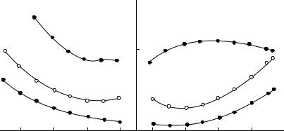
The influence of the SCR GR processes on the excess noise level is clearly confirmed by the measurements of the noise in the MOS structures with high leakage currents [15]. At the electric field intensity in the dielectric Eox = 106 V/cm (Ag = 0.2 mm2), the structures with the leakage currents I > 0.1 µA exhibit approximately the same excess noise levels for both polarities of the bias voltage. Figure 4 displays the SDs of the leakage current fluctuations versus the gate bias voltage for the MDS structures with leakage currents based on the KDB-4.5 silicon which are processed by different preoxidation techniques [15]. The noise levels in the enhancement and inversion modes are approximately identical regardless of the preoxidation processing technique applied to the silicon plates. This can be explained as follows. In these structures, the noise level depends, first of all, on the properties of the dielectric itself. According to [7], in the MDS structures with the high dielectric leakage current, the inversion layer is not formed because the SCR vanishes thus causing the absence of the GR processes in the SCR, which increase the excess noise level in the inversion mode. At the same time, in the MOS structures with high leakage currents, the trapping-type 1/f noise and the SCR
JOURNAL OF COMMUNICATIONS TECHNOLOGY AND ELECTRONICS Vol. 44 No. 12 1999
EXCESS NOISE IN METAL–DIELECTRIC–SEMICONDUCTOR STRUCTURES |
1307 |
||||||
|
|
|
S × 1028, A2 Hz– 1 |
|
|
|
|
|
3 |
|
|
|
|
|
|
|
|
|
102 |
|
|
3' |
|
2 |
|
|
|
|
|
2' |
|
|
|
|
|
|
|
|
|
1 |
|
|
|
|
|
1' |
|
|
|
|
|
|
|
|
|
|
|
|
101 |
|
|
|
|
– 7 |
– 5 |
– 3 |
– 1 0 1 |
3 |
5 |
7 U, V |
|
Fig. 4. SDs of the current fluctuations vs. the gate bias voltage for the MOS structures based on the KDB-4.5 p-type silicon with the leakage currents measured at T = 373K and f = 170 Hz; (1) and (1') the structures implemented on the plate treated with the combined cleaning (CC and PCT), and (2), (2'), (3), and (3') the structures treated with the CC.
GR noise may be masked by the higher-level noise due to the carrier transportation through the dielectric. The excess noise level in the structures with leakage cur-
rents (I > 10–6 A at Eox = 5 × 10⁵ V/cm) is several orders of magnitude greater than in the structures without
leakage currents [8, 15]. The leakage current can be caused by the presence of different kinds of defects in the dielectric film. As known, the structures with high leakage currents are characterized by an inhomogeneous dielectric layer containing microscopic regions with partially crystallized amorphous silicon, microspikes, protuberances on the dielectric surface, and so on [39].
According to the experimental data, the SD of the excess noise power is proportional to I2 for the structures with high leakage currents. This dependence is also typical for the MDS structures with dielectric macrodefects, such as pores and cracks [40]. For the structures with high leakage currents, the observed exponent of the spectrum is γ ≈ 1 . A similar result is obtained for the structures with the conductivity channels formed on chips [40].
The quadratic dependence of the SD of the 1/f noise power on the tunnel current is observed also for the MOS capacitors based on the n+-type silicon with the n+-polysilicon gate and the oxide 6.3- and 7.1-nm layers (Ag = 10–2 mm2) when the tunnel current density varies in the range jT = 1–4 nA/mm2 [19].
For the MDS structures with the ultrathin (tunnel) dielectric (hox = 2–4.5 nm) based on the n-type silicon
with the donor concentration 1015 cm–3, the dependence of the SD of the noise power on the current also approaches the quadratic function after the dielectric is damaged by high-intensity electric fields [22]. However, for the newly-fabricated MDS structures, before the dielectric damage, the behavior of the SD of the noise power substantially differs from the quadratic
function during the direct tunneling. Figure 5 displays the relative SD of the 1/f noise power versus the gate bias voltage for the MDS capacitor based on the n-type silicon with the n+Si* gate. These results are obtained for the structures with the undamaged and damaged dielectric [22]. The excess noise and the normalization current are measured at the same gate voltage. For the structures of both types, the observed noise level is by many orders of magnitude greater than the level predicted by the trapping model. According to [22], this difference is attributed to the carrier tunneling through the ultrathin dielectric.
The mechanisms of the excess noise generation in the structures with high leakage currents and structures without leakage currents are different. The MOS capacitor current flow is provided by the charge injection into the oxide where the charge can be trapped. In this case, the trap filling is governed by the current continuity condition [7] rather than by the Fermi–Dirac function. At the same time, in the structures with low leakage currents, the trapping mechanism of the flicker noise dominates, which is due to the charge fluctuations during the trapping and detrapping processes on the Si– SiO2 interface and in the oxide.
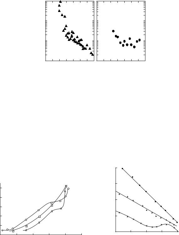
Figure 6 shows the SDs of the excess noise power versus the field intensity measured at 27 Hz for the MDS Al–SiO2–Si–Al structures (Ag = 1 mm2) with high leakage currents [8]. The SDs of the noise power monotonically increase with the field intensity in the range 105–5 × 10⁵ V/cm up to prebreakdown values. This effect is caused by the SiO2 macrodefects and, specifically, through pores [39]. In these structures, the dielectric breakdown occurs at EBD ≤ 106 V/cm. Structures of this kind exhibit the quadratic behavior of the SD of the noise power as a function of current.
Thus, the presented results demonstrate that the SD of the excess noise power due to the carrier transporta-
JOURNAL OF COMMUNICATIONS TECHNOLOGY AND ELECTRONICS Vol. 44 No. 12 1999
1308 |
|
ZHIGAL’SKII |
|
|
|
||
S/I2, Hz– 1 |
|
(a) |
|
|
(b) |
|
|
10– 7 |
|
|
|
|
|
|
|
10– 8 |
|
|
|
|
|
|
|
10– 9 |
|
|
|
|
|
|
|
10–10 |
2 |
3 |
4 |
1 |
2 |
3 |
4 |
1 |
|||||||
|
|
|
U, V |
|
|
|
|
Fig. 5. Relative SDs of the 1/f noise power of the MOS capacitor with the ultrathin dielectric vs. the gate voltage [22]: (a) undamaged dielectric, hox = 3.5 nm and (b) damaged dielectric, hox = 4.5 nm.
tion through the dielectric is proportional to squared dielectric leakage current I2 .
Figure 7 displays the frequency dependences of SDs of the noise power, whose behavior indicates the existence of different mechanisms of the excess noise generation in the MDS capacitors with different leakage currents. These SDs are measured for specially selected structures implemented on the KDB-4.5 plate in the depletion mode at the equal gate voltages U = –4 V [18]. One can see from the figure that the MDS structures with different leakage currents exhibit different characters of the noise spectrum. For the structure with a rel-
atively high leakage current (I = 0.5 µA), the high-level noise is observed, and SU( f) is the 1/f spectrum (curve 1). In these structures, the 1/f noise is due to the dielectric currents. At the same time, the structure with low leakage currents (I = 2.5 pA) exhibits a hump in the energy spectrum when f = 104–105 Hz (curve 3). A maximum in the noise spectrum at f ≈ 6 × 10⁴ Hz is also reported in [10] for the MDS structures operating in the depletion mode. These structures are based on the p-type silicon with the 50-nm oxide and 0.5-mm2 gate and have the leakage current I < 25 pA at the dielectric field intensity 8 MV/cm. The trapping theory of the
S × 1028, A2 Hz– 1
108 |
|
|
|
|
|
|
106 |
|
|
|
|
|
|
104 |
|
|
|
|
|
|
102 |
|
1 |
|
|
|
|
|
2 |
|
|
|
||
|
|
|
|
|
|
|
10 |
0 |
|
3 |
|
|
|
|
|
|
|
|
|
|
10– 2 |
2 |
4 |
6 |
8 |
10 |
|
|
0 |
|||||
Eox × 10– 5, V cm– 1
Fig. 6. SDs of the current fluctuations measured at 27 Hz vs. the field intensity for the Al–SiO2–Si–Al structures (Ag =
1 mm2) with high leakage currents, hox = (1) 50, (2) 50, and (3) 36 nm.
S × |
1028, A2 Hz– 1 |
|
|
|
|
107 |
|
|
|
|
|
105 |
|
|
1 |
|
|
|
|
|
|
|
|
|
|
2 |
|
|
|
103 |
|
|
|
|
|
|
|
3 |
|
|
|
101 |
|
|
|
|
|
10–1 |
101 |
102 |
103 |
104 |
105 |
|
|||||
|
|
|
|
|
f, Hz |
Fig. 7. SDs of the current fluctuations measured vs. frequency for the MOS structures based on the KDB-4.5 silicon with the p-type conductivity in the depletion mode with different leakage currents at the gate voltage U = –4 V (hox =
100 nm, Ag = 0.5 mm2); I = (1) 0.5 A, (2) 50 nA, and (3) 2.5 pA.
JOURNAL OF COMMUNICATIONS TECHNOLOGY AND ELECTRONICS Vol. 44 No. 12 1999

EXCESS NOISE IN METAL–DIELECTRIC–SEMICONDUCTOR STRUCTURES |
1309 |
excess noise, which is most extensively developed for the MDS transistor in [1], predicts the increase of SU(f) at high frequencies when the traps are nonuniformly distributed over energy in the oxide. For the p-channel MDS transistor, the increase of the noise spectrum flattening out in the frequency band f = 3 × 10³–104 Hz is observed in [41].
The existence of the maximum in the noise spectrum for the MDS capacitor (Fig. 7, curve 3) can be explained as follows. Because of the carrier trapping and detrapping, the charge fluctuations on the Si–SiO2 interface lead to the surface potential fluctuations. The carrier exchange between the ISs and oxide or silicon traps can be represented in the form of an equivalent electric circuit with capacitance Ct and resistance Rt connected in parallel (the RtCt circuit) [7]. The time constant RtCt is specified by the relaxation time of the trap filling. Taking into account the charge fluctuations on the Si–SiO2 interface, one can see that resistance Rt and capacitance Ct exhibit correlated fluctuations leading to the energy spectrum with the maximum at f = 1/2π RtCt . This frequency corresponds to the time constant of the trap recharging RtCt . The form of the spectrum similar to that shown in Fig. 7 is predicted in [35], where the linear RC circuit with flicker fluctuations of the resistance and capacitance is investigated theoretically. It should be noted that, when measuring the noise in the channel of the MDS transistor or diffusion resistor [29], correlated fluctuations of resistance Rt and capacitance Ct are not observed in the presence of the channel current. Therefore, in this case, the maximum in the noise spectrum also cannot be observed.
In [8], the correlation coefficients between the SD of the current fluctuations of the 1/f noise power S and squared leakage current I are calculated for the structures of three types with the gate area Ag = 1 mm2: the structures with the SiO2 36-nm (the first type) and 100-nm (the second type) dielectric layers as well as the MNOS structures with the 40-nm Si3N4 and 100-nm SiO2 layers (the third type). In the range of leakage currents (10–11–10–8) A, 200 structures of each type are investigated at the dielectric field intensity 6 × 10⁶ V/cm. The correlation coefficients R{S, I2} = 0.2, 0.44, and 0.46 are obtained for the structures of the third, second, and first types, respectively. The MNOS structures characterized by the lowest leakage currents exhibit the smallest correlation coefficient.
On the whole, the investigations of the MDS structures with the SiO2- and SiO2–Si3N4-based dielectric and the gates fabricated of different materials (Al, Mo, Si*) demonstrate that the excess noise is sensitive to the leakage currents only when j ≥ 10–8 A/mm2 . When j ≤ 10–13–10–9 A/mm2 , the 1/f noise of the MDS structures does not depend on the current. In this case, the current dependence of the SD of the noise power differs from the quadratic function, and the correlation between the
SD of the noise power and the leakage current is absent. This result confirms that the mechanism of the noise generated in the structures with low leakage currents is due to the charge trapping and detrapping in the oxide and on the Si–SiO2 interface rather than to the dielectric currents.
At the same time, in the structures with low leakage currents, a pronounced correlation between the breakdown field intensity and the excess noise level is observed when the fields approach the dielectric breakdown values.
Noise in the MDS Structures Operating
in High-Intensity Fields
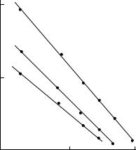
When measuring the SD of the noise power, potential U is applied to the gate to enhance the semiconductor surface with the majority carriers [7], i.e., in the case when the MDS structures are based on the p-type silicon, the gate is negatively biased to provide the electron injection from the gate into the dielectric. In this mode, capacitance Cx of the MDS structure is equal to oxide capacitance Ci specified by (6). The GR processes in the SCR of the silicon substrate do not affect the excess noise of the MDS capacitor, and therefore, the noise level is governed by the bulk properties of the dielectric as well as by the Si–SiO2 and SiO2–Me interfaces.
Figure 8 displays the typical SDs of the excess noise power versus the dielectric field intensity Eox = U/hox for the structures based on Ta2O5 [11] and the silicon oxide and for the MNOS structures with low leakage currents I = 10-11–10–9 A measured at Eox = 5 × 10⁶ V/cm, i.e., for the structures which do not contain
S × 1028, A2 Hz– 1 |
|
|
|
|
|
108 |
|
|
|
|
|
106 |
|
|
|
|
|
104 |
1 |
|
|
|
|
2 |
|
|
|
|
|
|
|
|
|
|
|
102 |
|
|
3 |
|
4 |
|
|
|
|
||
100 |
|
|
|
|
|
10– 2 |
2 |
4 |
6 |
8 |
10 |
0 |
|||||
|
|
|
Eox × |
10–6, V cm– 1 |
|
Fig. 8. SDs of the current fluctuations measured vs. the dielectric field intensity at 80 Hz for the Al–Ta2O5
(100 nm)–Si–Al structures with Ag = 0.75 mm2: (1) before annealing and (2) after annealing; (3) Al–SiO2 (100 nm)–
Si–Al (Ag = 1 mm2) and (4) MNOS Al–Si3N4 (40 nm)– SiO2(100 nm)–Si–Al structures.
JOURNAL OF COMMUNICATIONS TECHNOLOGY AND ELECTRONICS Vol. 44 No. 12 1999
1310 |
|
ZHIGAL’SKII |
|
||
S × 1028, A2 Hz– 1 |
|
|
In fact, the measured VCCs of the unannealed struc- |
||
103 |
|
|
tures [11] indicated the Ta2O5 film conductivity due to |
||
|
|
|
the Poole–Frenkel effect, which is caused by the dielec- |
||
3 |
|
|
tric trap ionization in the presence of the high-intensity |
||
|
|
field [7]. The mechanism of the excess noise generation |
|||
|
|
|
|||
|
|
|
in the Ta2O5-based structures due to the dielectric traps |
||
|
|
|
is also confirmed by the investigations of the noise in |
||
2 |
|
|
the Al–Ta2O5–Al structures [a metal–dielectric–metal |
||
101 |
|
|
(MDM) structure] In these structures, the dielectric lay- |
||
1 |
|
|
ers and gates are fabricated together with the MDS |
||
|
|
|
Al−Ta2O5–Si–Al structures in a single production |
||
|
|
|
cycle. It is found that the noise properties of the MDS |
||
|
|
|
and MDM Ta2O5-based structures are practically iden- |
||
|
|
|
tical [11]. In these structures, the noise level is mainly |
||
10– 1 |
|
|
governed by the dielectric leakage current due to the |
||
101 |
102 |
presence of the traps. |
|
||
100 |
Figure 9 presents the typical frequency dependences |
||||
|
|
|
|||
|
|
f, Hz |
of the SDs of the excess noise power for the Al– |
||
Fig. 9. SDs of the current fluctuations measured vs. fre- |
SiO2(100 nm)–Si–Al structures with comparatively |
||||
low leakage currents at different electric field intensi- |
|||||
quency for the Al–SiO2(100 nm)–Si–Al (Ag = 1 mm2) struc- |
|||||
ties in the dielectric [8]. One can see that these SDs |
|||||
tures at different dielectric field intensities; Eox = (1) 6 × |
exhibit the behavior of the 1/fγ spectrum. At small bias |
||||
106, (2) 6.5 × 10⁶, and (3) 7 × |
106 V/cm. |
|
|||
|
voltages, the exponent of the spectrum is γ ≈ |
1 , and it |
|||
|
|
|
increases with the field intensity approaching the value |
||
the poreand crack-type macrodefects in the dielec- |
γ ≈ 2–3 at the prebreakdown field intensities. The |
||||
tric [8]. |
|
|
increase of γ with the field intensity is also observed in |
||
The structures with the high-quality SiO2 dielectric or MNOS structures exhibit the low-level excess noise. For these structures operating in the enhancement mode, the noise level does not depend on intensity Eox in the range up to the prebreakdown values (Eox ≈ 5 ×
106–107 V/cm), which agrees with (5). This effect is due to the uniform trap distribution Nt over energy within the semiconductor bandgap for the majority charge carriers. At the same time, when the traps are nonuniformly distributed over the bandgap, a maximum may occur in the SD of the noise power considered as a function of U in both the enhancement [10] and inversion [17, 18] modes (Figs. 2, 3).
One can see from Fig. 8 that the Ta2O5-based structures exhibit a higher-level excess noise than the SiO2- and SiO2–Si3N4-based structures, especially those that are not annealed (curve 1). The Ta2O5 films are fabricated by the plasmachemical method and are characterized by a greater number of defects than the thermally grown SiO2 . When the field intensities differ significantly from the breakdown values, a high-level noise in the Ta2O5-based structures is due to the presence of the electron traps in the film. Since the number of these traps decreases after the structures are isothermally annealed (the annealing temperature is Tan = 400°C, the annealing time is tan = 30 min), the noise level decreases by one–two orders of magnitude after annealing (Fig. 8, curve 2). The Ta2O5 film conductivity is provided by the presence of the traps due to oxygen vacancies and impurities, which get into the film during its deposition.
the MOS SiO2-based structures with the Mo and n+Si* gate [9] and in the Ta2O5-based structures [11].
It is shown [42] that, just before the breakdown, a great number of defects are generated in the SiO2 layer, which behave as unstable electron traps. The increase of the concentration of the dielectric unstable traps, which is observed at the gate voltage approaching the breakdown value, leads to the noise increase. In the presence of high-intensity fields, the generation of the excess noise in the MDS structures can be caused by the charge fluctuations both in the dielectric itself and on the metal–dielectric and dielectric–semiconductor interfaces. As known, the processes developing on the Me–SiO2 interface affect the stability of the operation of the MDS devices [43, 44]. The density of the traps on the Me–SiO2 interface is extremely high and approach 1014cm–2 [45].
The influence of the Me–SiO2 interface on the excess noise level is confirmed by the investigations of the MOS structures implemented on the KDB-12 plates with the gates fabricated of Al, Mo, and polysilicon n+Si* [9]. The SiO2 dielectric for the structures of these three types is grown in a single production cycle. Statistical investigations of the MDS structures operating at the field intensity 8 MV/cm show that, at 20 Hz, the structures with the Mo gate exhibit the SD of the noise power which is by two–three orders of magnitude lower than the SD of the noise power observed in the structures with the Al gate and by an order of magnitude lower than the SD of the noise power observed in the structures with the polysilicon gate [9].
JOURNAL OF COMMUNICATIONS TECHNOLOGY AND ELECTRONICS Vol. 44 No. 12 1999