

ЛЕКЦИИ ФШФС_2007 / НАШИ СТАТЬИ / JCTE477_РЭ_5_05_Англ
.pdfNONDESTRUCTIVE QUALITY CONTROL OF INTEGRATED CIRCUITS |
487 |
Under ac conditions Al–Si(1%)–Cu(0.5%) films measuring 2 × 100 × 0.8 µm3 have values of γ in the range 0.85–1.15 [39]. This may explain the freedom from electromigration in a sinusoidal electric field [37].
At j0 higher than 106 or 107 A/cm2, voltage electromigration noise is characterized by the relation SV
jn, where n can take values of 3, 4, and even 7 [2]. This deviation from a quadratic relationship points to the noise being caused by nonequilibrium fluctuations in film conductance; mathematically, the noise should be linked to fluctuations in the coefficients Rn (n > 0) of
expansion (13). If j0 ≤ 106 A/cm2 , aluminum films exhibit ordinary equilibrium flicker noise, whose power spectral density varies as current density squared [18, 30, 40].
With a fixed j0 , the power spectral density of electromigration noise grows with temperature. Figure 7 illustrates this in the case of an Al–Si(1%) film examined at f0 = 0.05 and 1 Hz [11]. The figure also gives the values of γ corresponding to the two frequencies; they are obtained from logarithmic plots of SV( f ) over the frequency ranges 40–400 mHz and 0.5–1 Hz, respectively. It is seen at f0 = 1 Hz that electromigration noise is not detectable for any temperature considered. At f0 =
50 mHz electromigration noise is buried under a 1/f γ noise where γ = 0.9 to 1.1 and T ≤ 450 K; as the temperature is increased further, electromigration noise grows, with γ reaching 2 at T = 525 K.
The relationship between the power spectral density of voltage electromigration noise and the applied dc density j0 is written as
SV ( f ) = |
B j03 |
|
|
-------- |
(22) |
||
T f |
2 exp( Ea/kT ), |
||
|
|
|
|
where B is a constant; T is the temperature; and E‡ is the activation energy of electromigration, which is equal to that of the self-diffusion of metal atoms along grain boundaries, over the lattice, or along dislocations [10, 11, 41].
Equation (22) enables one to determine Ea from the power spectral density measured over a temperature range. For polycrystalline metal films, Ea has thus been found to correspond to the activation energy of grainboundary diffusion, which points to the diffusion process as the cause of electromigration noise [10, 11, 42]. More specifically, Ea = 0.6 eV for Al films examined over the temperature range 327–396 K [10]. For Al−Si(0.75%)–Cu(0.5%) films (thickness 0.8 µm, width 1.8 µm), the activation energy is in the range 0.58–0.77 eV [32]. Moreover, Koch et al. [43] have reported that, for films of aluminum or its alloys, both Ea and the activation energy of grain-boundary diffusion increase with the amount of doping. The reason for this may be that impurity segregation mainly occurs at grain boundaries when the impurity concentration is
S |
V |
( f ), V2/Hz |
|
|
|
|
|
|
|
|
|
|
|
|
|
|
|
|
|
|
|
|||||||||||
|
0 |
|
|
|
|
|
|
|
|
|
|
|
|
|
|
|
|
|
|
|
|
|
|
|
|
|
|
|
|
|
|
|
10– 13 |
|
|
|
|
|
1 |
|
|
|
|
|
|
|
|
|
|
|
|
|
2.0 |
||||||||||||
|
|
|
|
|
|
|
|
|
|
|
|
|
|
|
|
|
|
|||||||||||||||
|
|
|
|
|
|
|
|
|
|
|
|
|
|
|
|
|
|
|
|
|
||||||||||||
|
|
|
|
|
|
|
|
|
|
|
|
|
|
|
|
|
|
|
|
|
||||||||||||
10– 14 |
|
|
|
|
|
2 |
|
|
|
|
|
|
|
|
|
|
|
|
|
|||||||||||||
|
|
|
|
|
|
|
|
|
|
|
|
|
|
|
|
|
|
|||||||||||||||
|
|
|
|
|
|
|
|
|
|
|
|
|
|
|
|
|
|
|||||||||||||||
|
|
|
|
|
|
|
|
|
|
|
|
|
|
|
|
|
1.6 |
|
|
|||||||||||||
|
|
|
|
|
|
|
|
|
|
|
|
|
|
|
|
|
|
|
|
|
|
|||||||||||
|
|
|
|
|
|
|
|
|
|
|
|
|
|
|
|
|
|
|
|
|
|
|||||||||||
|
|
|
|
|
|
|
|
|
|
|
|
|
|
|
|
|
|
|
|
|
|
|
|
|
||||||||
|
|
|
|
|
|
|
|
|
|
|
|
|
|
|
|
|
|
|
|
|
|
|
|
|
|
|
|
|
|
|
|
|
10– 15 |
|
|
|
|
1.1 |
1.0 |
|
|
|
|
|
|
1.7 |
|
|
|||||||||||||||||
|
|
|
|
|
|
|
|
|
|
|
||||||||||||||||||||||
|
|
|
|
|
|
|
|
|
|
|
||||||||||||||||||||||
|
|
|
|
|
|
|
|
|
|
|
1.3 |
|
|
|||||||||||||||||||
|
|
|
|
|
|
|
|
|
|
|
||||||||||||||||||||||
|
|
|
|
|
|
|
|
|
|
|
|
|||||||||||||||||||||
0.9 |
|
|
|
|
||||||||||||||||||||||||||||
|
|
|
|
|
|
|
|
|
|
|
|
|
|
|
|
|
||||||||||||||||
|
|
|
|
1.2 |
|
|
|
|
|
|
|
|
|
|
||||||||||||||||||
|
|
|
|
|
|
|
|
|
|
|
|
|
|
|
|
|
|
|
|
|
|
|
|
|
|
|
|
|
|
|||
|
|
|
|
|
|
|
|
|
|
|
|
|
|
|
|
|
|
|
|
|
|
|
|
|
|
|
|
|
|
|||
|
|
|
|
|
|
|
1.0 |
|
|
|
1.1 |
|
|
|
|
|
|
|
|
|
|
|
|
|
|
|
|
|||||
10– 16 |
|
|
|
|
|
|
|
|
|
|
|
|
|
|
|
|
|
0.9 |
1.1 |
|||||||||||||
|
|
|
|
|
|
|
|
|
|
|
|
|
|
|
|
|
||||||||||||||||
|
|
|
|
|
|
|
|
|
|
|
|
|
|
|
|
|
|
|
|
|
|
|
|
|
|
|
||||||
|
|
|
|
|
|
|
|
|
|
|
|
|
|
|
|
|
|
|
|
|
|
|
|
|
|
|
|
|
|
|||
|
|
|
|
|
|
|
|
|
|
|
|
|
|
|
|
|
|
|
|
|
|
|
|
|
|
|
|
|
|
|||
|
|
|
0.9 |
0.9 |
1.0 |
|
|
|
|
|
1.1 |
|||||||||||||||||||||
|
|
|
|
|
|
|
|
|
|
|
||||||||||||||||||||||
|
|
|
|
|
|
|
|
|
|
|||||||||||||||||||||||
|
|
|
|
|
|
|
|
|
|
|
|
|
|
|
|
|||||||||||||||||
|
|
|
|
|
|
|
|
|
|
|
|
|
|
|
|
|||||||||||||||||
|
|
|
|
|
|
1.0 |
|
|
|
|
|
|||||||||||||||||||||
|
|
|
|
|
|
|
|
|
|
|
|
|
|
|
|
|
|
|
|
|
|
|
|
|||||||||
|
|
|
|
|
|
|
|
|
|
|
|
|
|
|
|
|
|
|
|
|
|
|
|
|||||||||
|
|
|
|
|
|
|
|
|
|
|
|
|
|
|
|
1.1 |
|
|
|
|
|
|
||||||||||
|
|
|
|
|
|
|
|
|
|
|
|
|
|
|
|
|
|
|
|
|
|
|||||||||||
|
|
|
|
|
|
|
|
|
|
|
|
|
|
|
|
|
|
|
|
|
|
|
|
|
|
|
|
|
|
|
||
|
|
|
|
|
|
|
|
|
|
|
|
|
|
|
|
|
|
|
|
|
|
|
|
|
|
|
|
|
|
|||
|
|
|
|
|
|
|
|
|
|
|
|
|
|
1.0 |
|
|
|
|
|
|
|
|
|
|
|
|
|
|||||
10– 17 |
|
|
|
|
1.0 |
|
|
|
|
|
|
|
|
|
|
|
|
|
|
|
||||||||||||
|
|
|
|
|
|
|
|
|
|
|
|
|
|
|
|
|
|
|
||||||||||||||
|
|
|
|
|
|
|
|
|
|
|
|
|
|
|
|
|
|
|
|
|
|
|||||||||||
|
|
|
|
|
|
|
|
|
|
|
|
|
|
|
|
|
|
|
|
|
|
|
|
|
|
|
|
|
|
|||
|
|
300 |
|
|
|
|
|
|
|
|
400 |
|
|
|
|
|
500 |
|
|
|||||||||||||
T, K
Fig. 7. Temperature dependence of power spectral density for 1/f 2 noise measured on an Al–Si(1%) film at f0 = (1) 0.05 and (2) 1 Hz with the film subjected to a current density of 3.4 MA/cm2 [11].
not too high ( 1 at. %), so the activation energy of grain-boundary self-diffusion should increase by an amount equal to the binding energy between an impurity atom and a vacancy [16]. Note also that impurities change the bulk properties of grains insignificantly.
Quite a different situation exists in metal films of submicrometer dimensions that have a monocrystalline structure or consist of grains whose mean size greatly exceeds the film width (bamboo structure), so that grain-boundary diffusion is nonexistent [1, 37]. In this case, activation energy E‡ as determined from Eq. (22) is greater than that of grain-boundary diffusion in polycrystalline films. For example, an activation energy of about 0.8 eV has been found in Al films (thickness 0.3– 0.45 µm, width 0.6–0.9 µm, length 400 µm) with a monocrystalline structure or with grains about 3 µm across, the measurements being made at a current density of 4 × 10⁶ A/cm2 [44]. The authors related this activation energy to diffusion along dislocations. Indeed, other workers have obtained 0.85 eV for the process [45, 46].
As already mentioned, a cubic relationship was observed between noise spectral density and current density for electromigration noise (Fig. 5). This indicates a correlation between R0(t) and R1(t), but the underlying mechanism has yet to be identified.
Additionally, voltage noise with SV j4, 3 has been observed in Al–Si–Ti(0.15%) films 1.2 µm long, 2.8 µm wide, and 1 µm thick over the temperature range 300–500 K and the current-density range (1–3) × 106 A/cm2 [4]. The noise varies with temperature according to the Arrhenius equation with E‡ = 0.59 eV at 3 × 10⁶ A/cm2 . The mean value of γ is 2.3, which is
JOURNAL OF COMMUNICATIONS TECHNOLOGY AND ELECTRONICS Vol. 50 No. 5 2005
488 |
ZHIGAL’SKII |
regarded as an indication of irrecoverable damage due to electromigration [4].
The above results show that electromigration noise is caused by the transport of metal atoms along grain boundaries, along dislocations, or over the lattice when the current density and temperature are high enough.
3. METHODS FOR EXPERIMENTAL STUDIES
OF NONEQUILIBRIUM FLICKER
FLUCTUATIONS IN CONDUCTING FILMS
AND CONTACTS
This section presents a brief discussion of two methods for extracting the nonequilibrium component of 1/f noise, in which different waveforms are used to drive the specimen [24, 25, 29]. More details are given in [9].
3A. Voltage Spectrum of the Signal Response in Film Sample under a Harmonic Test Action
If a |
film |
specimen is driven with the |
current |
I1 sin ω1t, |
its |
output voltage is written as |
U(t) = |
R(I1, t)I1 sinω1t. Taking into account approximation (13), |
|||
we obtain |
|
|
|
|
|
k |
|
U( t) |
= U0( t) + ∑ Un( t) sinnω1t, |
(23) |
|
n = 1
where U0(t) and Un(t) (n = 1, 2, 3, …, k) are random functions resulting from the fluctuations Rn(t) [25].
As the films and contacts of interest do not deviate greatly from Ohm’s law, we set k = 3 in Eq. (23), in which case U0 , U2 , and U3 are given by the following equations [25]:
U0( t) = 0.5R1( t) I12; |
(24) |
U2( t) = 0.5R1( t) I12; |
(25) |
U3( t) = 0.25R2( t) I13. |
(26) |
Furthermore,
U1( t) = R0( t) I1 + 0.75R2( t) I31 R0( t) I1. (27)
The fluctuations R0(t) are responsible for random amplitude modulation of the driving signal, which is known as 1/∆f noise [47–50]. This is an equilibrium phenomenon. The fluctuations in R1 and R2 affect U0 , U2 , and U3; they are responsible for nonequilibrium flicker noise. Equations (24)–(26) show that U0(t) and U2(t) are related to the quadratic nonlinearity of the cur-
rent–voltage characteristic: they are proportional to I21 .
Note also that U3(t) is related to the cubic nonlinearity, being proportional to I31 .
The nonlinear behavior of a current–voltage characteristic is mostly characterized by the third-harmonic distortion
KN = U3/U1. |
(28a) |
This is expressed in decibels as [51] |
|
KN = 20log( U3/U1 ). |
(28b) |
One may also consider the second-harmonic distortion
KN2 = |
U2 |
KN2 |
= 20log |
U2 |
------; |
------ (in dB) . (28c) |
|||
|
U1 |
|
|
U1 |
3B. Method
for Measuring Amplitude Fluctuation Spectra of Signal-Response Harmonics
in a Sample under a Harmonic Test Action
Methods for investigating the amplitude fluctuations of sinusoidal signals are described in the monograph by Malakhov [52]. When studying nonequilibrium flicker noise, one usually measures the power spectral densities of U3(t), U2(t), or U0(t) [9, 25].
This task entails detecting the amplitude fluctuations. Note that the detector will receive a discrete spectrum with a symmetrical pedestal about each line as a result of amplitude fluctuations [52]. The output spectrum consists of a band centered at the zero frequency [52].
Below we briefly describe an instrument for measuring the power spectral density of fluctuations in the dc component and in the amplitudes of the first to third harmonic components of a voltage response to sinusoidal current driving. This instrument was used to examine nonequilibrium flicker noise in Mo films [9, 25].
The instrument is made up of six units:
(i)a sinusoidal generator for driving specimens. An output low-pass filter ensures very low harmonic distortion (<–150 dB). The output frequency may be set to f1 = 10 kHz [25];
(ii)a frequency-selective amplifier designed to extract a response signal at f1 [47–50];
(iii)high-sensitivity frequency-selective amplifiers for extracting and enhancing a response signal at 2f1 ,
3f1 , or 0, as appropriate. In the first two cases, the amplifier is preceded by a high-pass filter to reject frequency components close to f1;
(iv) an amplitude detector for the f1 , 2f1 , and 3f1 harmonic components that have been modulated in amplitude by the nonequilibrium flicker noise being examined;
JOURNAL OF COMMUNICATIONS TECHNOLOGY AND ELECTRONICS Vol. 50 No. 5 2005
NONDESTRUCTIVE QUALITY CONTROL OF INTEGRATED CIRCUITS |
489 |
(v)the detector is followed by low-pass filters designed to pass only frequency components that are low compared with f1; and
(vi)the low-pass filters are followed by a high-sen- sitivity low-frequency amplifier.
The output of the instrument is processed with a spectrum analyzer or computer.
The obtained power spectral densities of U0(t), U2(t), and U3(t) allow one to determine those of R1(t), R2(t), and R3(t) from to Eqs. (24)–(26).
3C. Method for Measuring Voltage Fluctuations
of the DC Component of the Sample’s Signal Response under a Pulsed Test Action
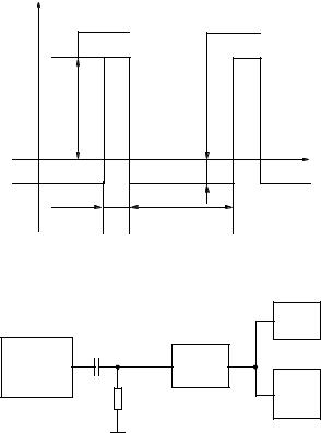
Instead of a sinusoidal signal, one may apply a bipolar train of rectangular current pulses of uniform height and zero mean as shown in Fig. 8. The response of a nonlinear circuit to such driving will have a fluctuating dc voltage component Udc .
Figure 9 shows a simple arrangement for measuring Udc and the power spectral density of its fluctuations [24]. Driving pulse trains are applied to a specimen via blocking capacitance C. A low-pass filter serves to extract Udc . The level of the voltage is measured with a voltmeter and its fluctuations are processed with a spectrum analyzer or computer. The nonequilibrium flicker noise component is thus extracted. Note that if the specimen resistance does not vary with current, then Udc = 0.
Testing with a pulsed signal is useful for the following reasons presented in [24, 53].
To avoid overheating of the specimen, the driving pulse train should be such that
Q = Tp /τV1 2, |
(29) |
where τV1 is the width of a positive-going pulse and Tp is the pulse repetition period (Tp = τV1 + τV2).
Assume that Udc does not depend on Tp or τV1.
It can be shown for constraints (17) and (29) that the nonlinear right-hand term of Eq. (15) is proportional to Udc [24, 53]. More specifically,
N(I, t)I [Q3/(Q – 2)(Q – 1)]U |
(I |
, t). |
(30) |
dc |
p |
|
|
It is advantageous to set Q = 12, in which case Eq. (30) becomes
IV (t) |
|IV1| |
|IV 2| |
|
Ip |
|
0 |
|
t |
|
τV1 |
τV2 |
Fig. 8. Driving pulse train.
|
|
|
3 |
|
C |
|
Udc |
1 |
|
|
|
|
|
2 |
|
|
|
R |
4 |
|
|
|
Fig. 9. Arrangement for measuring Udc and the power spec-
tral density of its fluctuations: (R) specimen, (1) drivingpulse generator, (2) low-pass filter, (3) voltmeter, and (4) spectrum analyzer [24].
Equations (30) and (32) can be used to evaluate
N(I, t) and SVN( f ).
For ICs an increase in Udc may be indicative of the following faults:
(i)inhomogeneities in contacts, resistor films, and metallization patterns;
(ii)thin dielectric layers at contacts or metal grain boundaries (they act as barriers to electrical transport); and
(iii)pores and stressed regions in interconnections and at contacts.
The spectrum of fluctuations in Udc can be used to detect instability of contacts and metal films due to corrosion, solid-state chemical reactions, or time-depen- dent stress [1, 28].
N(I, t)I 12Udc(Ip , t). |
(31) |
4. NONDESTRUCTIVE IC QUALITY CONTROL |
|
|
USING TEST STRUCTURES |
It follows that the respective power spectral densities SVN( f ) and Sdc( f ) of nonequilibrium 1/f noise and the fluctuations in Udc are linked by the equation [24]
S |
VN |
( f ) [Q3/(Q – 2)(Q – 1)]2S ( f ). |
(32) |
|
dc |
|
The reliability of ICs and their individual passive elements can be predicted from measurements of 1/f- noise level and nonlinearity parameters. This nondestructive approach applies to different types of IC, including monolithic, microwave hybrid, and flip-chip
JOURNAL OF COMMUNICATIONS TECHNOLOGY AND ELECTRONICS Vol. 50 No. 5 2005
490 |
|
|
|
|
|
|
|
|
|
|
|
|
|
|
ZHIGAL’SKII |
|
|||
α |
|
|
|
|
|
|
|
|
|
|
|
|
|
|
|
gration-induced faults, the films having been subjected |
|||
103 |
|
|
|
|
|
|
|
|
|
|
|
|
|
|
|
to high temperature and current stresses. |
|
||
|
|
|
|
|
|
|
|
|
|
|
|
|
|
|
|
||||
|
|
1 |
|
|
|
|
|
|
|
|
|
|
|
This section gives an overview of experimental |
|||||
|
|
|
|
|
|
|
|
|
|
|
|
|
|
|
|
|
results concerning different methods of nondestructive |
||
|
|
|
|
|
|
|
|
|
|
|
|
|
|
|
|
|
|||
|
|
2 |
|
|
|
|
|
|
|
|
|
|
|
|
|
quality control by measurement of equilibrium or non- |
|||
|
|
|
|
|
|
|
|
|
|
|
|
|
|
|
equilibrium flicker noise and nonlinearity parameters in |
||||
|
|
|
|
3 |
|
|
|
|
|
|
|
|
|
|
|
||||
|
|
|
|
|
|
|
|
|
|
|
|
|
|
||||||
101 |
|
|
|
|
4 |
|
|
|
|
|
|
|
|
|
|
the context of metal films and contacts. |
|
||
|
|
|
|
|
|
|
|
|
|
|
|
|
|
|
|||||
|
|
|
|
|
|
|
|
|
|
|
|
|
|
|
|
|
|
||
|
|
|
|
|
|
|
|
5 |
|
|
|
|
|
|
|
|
4A. Electromigration Immunity Prediction |
|
|
|
|
|
|
|
|
|
|
|
|
|
|
|
|
|
|
|
|
||
|
|
|
|
|
|
|
|
|
|
|
|
|
|
|
|
|
|
||
|
|
|
|
|
|
|
|
|
|
|
|
|
|
|
|
|
by 1/f Noise |
|
|
10– 1 |
|
|
|
|
6 |
|
|
|
|
|
|
|
Potemkin et al. [58] proposed using vacancy- |
||||||
|
|
|
|
|
|
|
|
|
|
||||||||||
|
|
|
|
|
|
|
7 |
|
|
|
|
|
|
induced equilibrium 1/f noise for the prediction of the |
|||||
|
|
|
|
|
|
|
|
|
|
|
|
|
|
||||||
|
|
|
|
|
|
|
|
|
|
|
|
|
|
|
8 |
|
immunity of Al thin films to electromigration. The |
||
|
|
|
|
|
|
|
|
|
|
|
|
|
|
|
|
||||
|
|
|
|
|
|
|
|
|
|
|
|
|
|
|
|
|
method is based on the experimental finding that 1/f |
||
|
|
|
|
|
|
|
|
|
|
|
|
|
|
|
|
|
|||
αH |
|
|
|
|
|
|
|
|
|
|
|
|
|
|
|
noise is stronger in films with smaller grains [18, 40]. |
|||
|
|
|
|
|
|
|
|
|
|
|
|
|
|
|
|||||
10 |
– 3 |
|
|
|
|
|
|
|
|
|
|
|
|
|
|
|
Figure 10 presents experimental data on how 1/f-noise |
||
|
|
|
|
|
|
|
|
|
|
|
|
|
|
|
|||||
50 |
|
|
100 |
|
|
150 |
200 davg , nm |
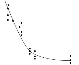
level varies with mean grain size davg in Al films [6]. It |
|||||||||||
Fig. 10. Variation of 1/f-noise level with mean grain size in |
is seen that the noise level grows by three orders of |
||||||||||||||||||
magnitude if davg is reduced by half. This growth is |
|||||||||||||||||||
Al films [6]. Points 1–4 refer to films produced at different |
|||||||||||||||||||
deposition rates. Points 5–8 refer to films produced at dif- |
accompanied by an increase in the proportion of grains |
||||||||||||||||||
ferent Ar pressures. Points lying on the same segment refer |
with davg ≤ 50 nm, as revealed by comparison of grain- |
||||||||||||||||||
to films of the same batch. The dashed line represents the |
size distribution curves. Moreover, Al thin-film inter- |
||||||||||||||||||
Hooge constant αH = 2 × 10⁻³. |
|
|
|
|
|
|
connections with smaller grains are known to have a |
||||||||||||
|
|
|
|
|
|
|
|
|
|
|
|
|
|
|
|
|
shorter median time until failure due to electromigra- |
||
circuits. These IC’s passive elements include thin-film |
tion [37]. These results provide strong evidence that |
||||||||||||||||||
vacancy-induced equilibrium 1/f noise can be used to |
|||||||||||||||||||
interconnections, contacts, |
film |
resistors, and MOS |
|||||||||||||||||
assess the electromigration immunity of metal films. |
|||||||||||||||||||
structures. |
|
|
|
|
|
|
|
|
|
|
|
||||||||
|
|
|
|
|
|
|
|
|
|
|
The power spectral density of equilibrium flicker |
||||||||
Investigations have shown that nonequilibrium |
|||||||||||||||||||
noise (see Eq. (9b)) varies with temperature according |
|||||||||||||||||||
flicker noise is often more informative than equilibrium |
to the Arrhenius equation, in which the activation |
||||||||||||||||||
flicker noise, particularly with respect to lattice imper- |
energy is equal to that of vacancy creation, Evac . This |
||||||||||||||||||
fections. Nonequilibrium flicker noise can serve as a |
provides a way to find Evac . With electromigration |
||||||||||||||||||
very sensitive detector of latent defects. |
immunity testing, the median time until failure t50 is |
||||||||||||||||||
On the other hand, vacancy-induced equilibrium |
calculated by |
|
|||||||||||||||||
flicker noise can sometimes (but not always) be used to |
t50 = A1 jn exp( Ea/kT ), |
(33) |
|||||||||||||||||
assess the stability of contacts and film resistors as well |
|||||||||||||||||||
as the immunity of thin-film interconnections to elec- |
where A1 depends on the material, structure, |
and |
|||||||||||||||||
tromigration (see Section 1B). |
|
|
|
|
|||||||||||||||
|
|
|
|
dimensions of the film and E‡ is the activation energy of |
|||||||||||||||
Sikula et al. [54, 55] addressed the issue of 1/f-noise |
|||||||||||||||||||
vacancy self-diffusion [37]. |
|
||||||||||||||||||
quality assessment and reliability prediction in the con- |
As j is increased, exponent n remains equal to 1 for |
||||||||||||||||||
text of thick conducting films of Ag–Pd or Ag pastes. |
|||||||||||||||||||
small current densities (j ≤ 105 A/cm2) and grows with |
|||||||||||||||||||
They detected |
a flicker-noise |
component with an |
|||||||||||||||||
an increase in the current density, usually taking values |
|||||||||||||||||||
exactly 1/f spectrum, for which S I02 , and an excess |
|||||||||||||||||||
from 1–5 [38]. |
|
||||||||||||||||||
noise component having a 1/f γ spectrum with γ ≈ 1.4. |
It is known that diffusion in metals occurs mainly by |
||||||||||||||||||
The latter is produced by defects and can serve to detect |
the vacancy mechanism [16, 17]. In Eq. (33) Ea = Evac + |
||||||||||||||||||
them. However, its mechanism has not been identified. |
Em , where Evac and Em are the activation energies of |
||||||||||||||||||
It may be that the excess noise is identical to nonequi- |
vacancy creation and migration, respectively. Conse- |
||||||||||||||||||
librium flicker noise. |
|
|
|
|
|
|
quently, Ea will decrease with a decrease in Evac , so that |
||||||||||||
It is advantageous to perform 1/f-noise characteriza- |
the noise level will grow (see Eqs. (9b) and (10)). Elec- |
||||||||||||||||||
tion of active and passive elements in conjunction with |
tromigration immunity prediction by equilibrium 1/f |
||||||||||||||||||
harmonic-distortion measurements. For example, Sed- |
noise is possible because Evac varies with grain size, |
||||||||||||||||||
lakova et al. [56] used 1/f conductance fluctuations and |
being lower in films with smaller grains. This means |
||||||||||||||||||
the third harmonic distortion to assess the stability of |
that energy Ea is less in films with small grain size. It is |
||||||||||||||||||
thick-film resistors. Jones and Xu [57] related the sec- |
this effect that allows estimation of the electromigra- |
||||||||||||||||||
ond and third harmonic distortions to excess-noise level |
tion immunity of thin-film conductors by the level of |
||||||||||||||||||
for Al–Cu(4%) films 1 µm thick containing electromi- |
the vacancy-induced equilibrium 1/f noise. |
|
|||||||||||||||||
JOURNAL OF COMMUNICATIONS TECHNOLOGY AND ELECTRONICS Vol. 50 No. 5 2005
NONDESTRUCTIVE QUALITY CONTROL OF INTEGRATED CIRCUITS |
491 |
However, measurement of equilibrium flicker noise does not allow one to determine Ea or to predict the electromigration immunity of metal films with a low density of mobile defects. Under relatively low current densities, equilibrium 1/f noise is produced by acousticphonon scattering in such films, with the power spectral density given by Eq. (1).
There is a considerable body of work providing evidence for a relationship between electromigration immunity and the level of 1/f 2 noise for metal thin films [10, 11, 30–36, 39, 57]. This relationship is due to the fact that defects act as sources and sinks of vacancies [16] and, as such, influence both the noise and electromigration immunity of films [37]. As a result 1/f 2 noise should grow with defect density. Indeed, Chen et al. [59] confirmed by direct measurement that Al films with an elevated level of excess noise display a shorter median time until failure. Later Neri et al. [10] used 1/f 2-noise–temperature relations to determine the activation energy for Al films. This has been found to be about 0.67 eV, which corresponds to the activation energy of vacancy self-diffusion along grain boundaries. This value is consistent with those obtained by other methods.
To measure 1/f 2 noise, high current and temperature are required in order for its power spectral density to be greater than that of the overall flicker noise [10, 11]. Under dc current, 1/f 2 noise is stronger than equilibrium 1/f noise (γ ≈ 1) only at frequencies below 1 Hz; the range of measurement may extend into the millihertz region.
Accordingly, 1/f 2 noise should be examined with the help of special techniques of extracting 1/f 2 noise, such as those in Section 3. A sinusoidal driving signal is sometimes used in addition to a direct current of high density [57]. Testing with a pulsed signal [24, 26] appears to be more suitable for industrial conditions, because it can be implemented more easily.
In any case both vacancy-induced equilibrium 1/f noise and electromigration-induced nonequilibrium 1/f 2 noise can be used for early detection of electromi- gration-induced damages in metal thin films when other methods fail. Moreover, the former type of noise allows one to rapidly assess immunity to electromigration. It offers an alternative to time-consuming and expensive bias–temperature stressing.
4B. Forecasting Long-Term Stability of Metal–Semiconductor Ohmic Contacts as Predicted by 1/f Noise and Nonlinearity
of CVC Parameters
Below we report the results of an experiment on test chips, each chip containing a chain of 196 metal–semi- conductor or metal–metal contacts in series. The dimensions of the contacts are the same for all the chips. Contact is made through a window measuring
S × 1016, Hz– 1 |
|
|
|
104 |
|
|
|
103 |
1 |
2 |
|
|
|
||
|
|
3 |
|
|
|
4 |
|
102 |
|
|
|
|
5 |
|
|
|
6 |
|
|
101 |
102 |
103 |
104 |
|
|
|
f, Hz |
Fig. 11. Power spectral density of 1/f noise for chains of 196
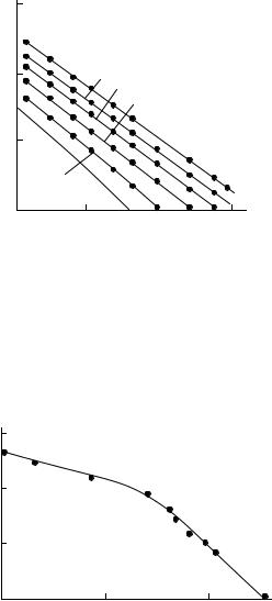
Al–Si(1%)/n+-Si or Al–Si(1%)/Al–Si(1%) ohmic contacts [60]. Lines 1–4 refer to the metal–semiconductor structures (1) with unprepared contact windows or (2–4) with those prepared by three different techniques. The structures represented by line 4 are subjected to amorphization by ion implantation. Line 5 represents metal–metal contacts. Lines 1–5 were obtained by measurement. Line 6 was calculated by Eq. (1).
KN, dB
–70
–90
– 110
– 130 |
101 |
102 |
100 |
NP × 10– 18, cm– 3
Fig. 12. Third-harmonic distortion vs. phosphorus concentration for Al–Si(1%)/n+-Si ohmic contacts.
5 × 5 or 4 × 4 µm2 , respectively, etched in a SiO2 layer. The chips are made from a Si(100) wafer. The metal– semiconductor contacts are produced by phosphorus or boron doping to 8 × 1019 cm–3. The junction depth is 1.2 µm, and the semiconductor sheet resistance in the contact region is 5–30 Ω/ .
The metal layers are made from an Al–Si(1%) alloy by magnetron sputtering [1, 28]. In the metal–metal structure, the first metallization layer is 0.6 µm thick. The other metal layers are of thickness 0.9–1.0 µm.
Four batches were examined, differing in the technique by which the contact-window bottom is prepared for metal deposition. Figure 11 displays measured (1–5)
JOURNAL OF COMMUNICATIONS TECHNOLOGY AND ELECTRONICS Vol. 50 No. 5 2005
492 |
|
|
|
|
|
|
|
|
|
ZHIGAL’SKII |
|
||||
KN, dB |
|
|
|
|
|
|
|
|
|
Comparison of Figs. 11 and 13 indicates a marked |
|||||
|
|
|
2 |
|
3 |
|
4 |
|
|
|
|
correlation between 1/f-noise level and third-harmonic |
|||
|
1 |
|
|
|
|
|
|
||||||||
– 80 |
|
|
|
|
|
|
|
|
|
|
|
|
distortion for a range of processing techniques. Note |
||
|
|
|
|
|
|
|
|
|
|
|
|
that the noise and harmonic distortion are lowest in the |
|||
|
|
|
|
|
|
|
|
|
|
|
|
||||
|
|
|
|
|
|
|
|
|
|
|
|
|
case of argon-ion treatment (see lines 4), because this |
||
|
|
|
|
|
|
|
|
|
|
|
|
|
provides a highly irregular surface on the bottom of a |
||
– 100 |
|
|
|
|
|
|
|
|
|
5 |
|
|
contact window, increasing the effective contact area |
||
|
|
|
|
|
|
|
|
|
|
|
|||||
|
|
|
|
|
|
|
|
|
|
|
|
and improving the electrical and thermal characteristics |
|||
|
|
|
|
|
|
|
|
|
|
|
|
|
|||
|
|
|
|
|
|
|
|
|
|
|
|
|
of the contact. |
|
|
– 120 |
|
|
|
|
|
|
|
|
|
|
|
|
Furthermore, a link was established between long- |
||
|
|
|
|
|
|
|
|
|
|
|
|
||||
|
|
|
|
|
|
|
|
|
|
|
|
||||
0 |
|
1 |
|
|
2 |
I0, mA |
term reliability and third-harmonic distortion for |
||||||||
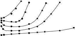
Fig. 13. Measured dc dependence of third-harmonic distor- |
metal–semiconductor ohmic contacts [60]. The mea- |
||||||||||||||
surements were carried out on 33 randomly chosen |
|||||||||||||||
tion for chains of 196 Al–Si(1%)/n+-Si or Al–Si(1%)/Al– |
|||||||||||||||
chips with B-doped Al–Si(1%)/n+-Si contacts. The con- |
|||||||||||||||
Si(1%) [60]. Lines 1–4 refer to the metal–semiconductor |
|||||||||||||||
structures (1) with |
unprepared |
|
contact |
windows or |
tact region is characterized by a doping concentration |
||||||||||
(2−4) with those prepared by three different techniques. |
of 8 × 1019 cm–3 and a semiconductor sheet resistance |
||||||||||||||
The structures represented by line 4 are subjected to amor- |
of 9 Ω/ . Reliability was assessed by 264-h bias–tem- |
||||||||||||||
phization by ion implantation. Line 5 represents the metal– |
|||||||||||||||
perature stressing at 5 × 10⁵ A/cm2 and 398 K. The mea- |
|||||||||||||||
metal contacts. The measurements were made at f1 = |
|||||||||||||||
0.2 MHz and U1 = 250 mV. |
|
|
|
|
|
|
|
sured characteristics were the prestress third-harmonic |
|||||||
|
|
|
|
|
|
|
|
|
|
|
|
|
distortion KN(0) (t = 0), the prestress contact resistance |
||
and calculated (6) power spectral densities of 1/f noise |
RC(0), and the poststress contact resistance RC(t). Aging |
||||||||||||||
was evaluated by the ratio |
|
||||||||||||||
for the contact chains [60]. Lines 1–4 refer to metal– |
KR(t) = [RC(t) – RC(0)]/RC(0). |
(34) |
|||||||||||||
semiconductor (n+-Si) structures with unprepared win- |
|||||||||||||||
dows (line 1) or with windows prepared by three differ- |
A correlation coefficient of 0.95 was found between |
||||||||||||||
ent techniques. The structures represented by line 4 are |
|||||||||||||||
subjected to amorphization by 20-keV argon-ion |
KN(0) and KR(t) (t = 264 h), indicating strong correla- |
||||||||||||||
implantation to a dose of 150 µC/cm2 (optimal condi- |
tion between long-term reliability and prestress third- |
||||||||||||||
tions). Line 5 is for metal–metal contacts. Line 6 is cal- |
harmonic distortion. A reason for this may be that the |
||||||||||||||
culated by Eq. (1) with the effective volume of the con- |
original thermal instability of contacts, due to micro- |
||||||||||||||
tact region being taken as 6 × 10–12 cm3 (nc = 1.8 × |
scopic structural defects, manifests itself in harmonic |
||||||||||||||
1023 cm–3). It is seen that Eq. (1) provides an accurate |
distortion and leads to contact-resistance degradation |
||||||||||||||
approximation in the case of metal–metal contacts, the |
under stressing. |
|
|||||||||||||
The relationship between the 1/f-noise level and har- |
|||||||||||||||
minor errors being attributable to an error in the effec- |
|||||||||||||||
tive volume or to the vacancy-induced equilibrium 1/f |
monic distortion in ohmic contacts makes it possible to |
||||||||||||||
noise of the contacts. |
|
|
|
|
|
|
|
|
|
test their reliability by measuring third-harmonic dis- |
|||||
The contacts were also assessed in terms of third- |
tortion rather than noise. As the former approach uses a |
||||||||||||||
deterministic signal, it appears to be more suitable for |
|||||||||||||||
harmonic distortion. This was measured as a function |
|||||||||||||||
industrial applications. |
|
||||||||||||||
of the direct current I0 by 0.2-MHz sinusoidal driving |
|
||||||||||||||
Gradual failures of ICs often stem from degradation |
|||||||||||||||
such that the fundamental-harmonic amplitude U1 was |
|||||||||||||||
of ohmic contacts caused by intrinsic factors or operat- |
|||||||||||||||
held at 250 mV. |
|
|
|
|
|
|
|
|
|
||||||
|
|
|
|
|
|
|
|
|
ing conditions. The harmonic-distortion–reliability |
||||||
Third-harmonic distortion was also calculated by |
|||||||||||||||
relationship appears to be linked to unstable micro- |
|||||||||||||||
Eq. (28b). |
|
|
|
|
|
|
|
|
|
scopic structural defects originally present in contact |
|||||
Figure 12 is the third-harmonic distortion plotted |
regions, such as vacancies in the metal film. These con- |
||||||||||||||
tribute to the harmonic distortion according to Eq. (11). |
|||||||||||||||
against the concentration of the doping impurity in the |
|||||||||||||||
The degradation is mainly due to diffusion of impurities |
|||||||||||||||
semiconductor, NP. The fact that the harmonic distor- |
|||||||||||||||
[61], particularly doping impurities, from the semicon- |
|||||||||||||||
tion falls with an increase in the doping level, especially |
|||||||||||||||
ductor to the metal. An increased vacancy density in the |
|||||||||||||||
in the range (0.1–5.0) × 1020 cm–3, indicates the forma- |
|||||||||||||||
film will enhance the diffusion. As a result, the semi- |
|||||||||||||||
tion of an ohmic contact. Thus, third-harmonic distor- |
|||||||||||||||
conductor surface becomes depleted of impurities and |
|||||||||||||||
tion can be used to estimate the quality of ohmic con- |
|||||||||||||||
the contact resistance grows (see above). |
|
||||||||||||||
tacts on chips. |
|
|
|
|
|
|
|
|
|
|
|||||
|
|
|
|
|
|
|
|
|
The reliability prediction of ohmic contacts is a |
||||||
Figure 13 shows the variation of third-harmonic dis- |
|||||||||||||||
major issue in microelectronics manufacturing. It fol- |
|||||||||||||||
tortion with I0 [60]. Lines 1–4 refer to metal–semicon- |
lows from the discussion above that this task may be |
||||||||||||||
ductor (n+-Si) structures with unprepared contact win- |
approached by measuring 1/f noise or harmonic distor- |
||||||||||||||
dows or with windows prepared by three different tech- |
tion on test contact structures that can be formed simul- |
||||||||||||||
niques. Line 5 is for metal–metal contacts. |
|
|
|
taneously on a wafer and contact pads. |
|
||||||||||
JOURNAL OF COMMUNICATIONS TECHNOLOGY AND ELECTRONICS Vol. 50 No. 5 2005
NONDESTRUCTIVE QUALITY CONTROL OF INTEGRATED CIRCUITS |
493 |
Another conclusion is that measuring third-har- monic distortion on unstressed contacts as a method for testing long-term reliability is clearly more advantageous than accelerated life testing because it is rapid and inexpensive.
4C. Bond-Strength Prediction by 1/f Noise
In this subsection we discuss an experiment on bond-strength prediction using test contacts [63] made by thermocompression bonding [62]. Such bonds are used in microwave hybrid ICs. The test structure is a 50-µm gold wire bonded to a copper contact pad with an area of 0.6 × 0.6 mm2 and a thickness of 6 µm on a devitrified-glass substrate. Different bonding conditions were applied. The test specimens were fabricated as half-bridges in which each arm contained two bonds. Buses of three gold wires in parallel were used to connect contact pads to package leads in order to reduce 1/f noise in the pad–lead interconnections.
Bonding conditions have been found to influence the 1/f noise and harmonic distortion of the bonds. The power spectral density of the noise was measured on asprepared specimens. Then the specimens were kept under normal conditions for ten days before being subjected to a bond-pull test. A connection has thus been discovered between the noise level in as-prepared specimens and the bond strength [63]. More specifically, bond strength is found to increase with a decreasing noise level in the case where detachment occurs along the border of the bonded area or where pulling results in bond peel.
It is known that as-cooled weld seals are characterized by an elevated vacancy density and may contain vacancy complexes, the vacancy density varying with welding conditions [62]. This accounts for the higher level of 1/f noise in specimens of lower bond strength. Moreover, it is fluctuations in excess-vacancy density that are responsible for the 1/f noise observed (see Section 1). The excess vacancies can eventually form microand macroscopic pores [1, 28] to reduce the bond strength.
Thus, 1/f-noise measurement enables one to optimize thermocompression-bonding conditions for microwave hybrid ICs.
4D. Solder-Bonding Quality Control
by the DC Component of the Voltage Response to a Pulsed Test Action
This subsection reports on an experimental investigation into the quality control of solder bonding. Test specimens were fabricated that contained a chain of 20 identical soldered bonds. These specimens were based on a general-purpose flip-chip assembly in which the contacts on a chip were joined to the corresponding polyimide-contact structure (50 µm thick) using POS-61 solder [64]. The flip-chip assembly was
Solder-bonding quality control: the contact resistance R and the dc component Udc of voltage response for test specimens based on a general-purpose flip-chip assembly. Each specimen contains a chain of 20 identical soldered bonds
Specimen no. |
R, Ω |
Udc , µV |
|
|
|
1 |
4.68 |
18.49 |
2 |
4.34 |
16.62 |
3 |
4.28 |
372 |
4 |
4.13 |
16.20 |
5 |
3.97 |
16.37 |
6 |
3.97 |
21.12 |
7 |
3.88 |
16.69 |
8 |
3.39 |
17.06 |
9 |
3.30 |
15.39 |
10 |
3.88 |
18.78 |
11 |
3.69 |
17.29 |
12 |
4.10 |
17.72 |
13 |
4.20 |
19.60 |
14 |
4.22 |
18.55 |
15 |
4.67 |
2885 |
16 |
4.45 |
17.97 |
17 |
4.25 |
16.43 |
18 |
4.47 |
19.14 |
19 |
4.40 |
17.30 |
|
|
|
designed by the Mnogokristal’nye Tekhnologii Company, Zelenograd, Russia.
For 19 specimens, the dc component Udc of voltage response to pulsed driving was measured at room temperature, as in Section 3C. The driving pulse train had τV1 = 16 µs and Q = 10 (see Fig. 8). The results are presented in the table.
Specimens have been found that differed in Udc by more than two orders of magnitude while having close contact resistances. The table shows that the dc voltage component and contact resistance vary over the ranges 15.39–2885 µV and 3.30–4.68 Ω , respectively. Furthermore, specimens 3 and 15 are unique in having values of Udc as high as 372 and 2885 µV, respectively.
Figure 14 is a graph of Udc against τV1 at Ip = 0.5 A [3]. The strong nonlinearity of the CVC can be attributed to
different types of latent defects in the solder bonds (inhomogeneities, pores, thin dielectric layers, corrosion, and local stresses). The defects mainly affect Udc and slightly influence R. Notice that the specimens with strongly nonlinear CVCs display insignificant variation of Udc with τV1. The other specimens (R = 3.30 to 4.68 Ω) exhibit marked dependence of Udc on τV1 , indicating thermal diffusion.
JOURNAL OF COMMUNICATIONS TECHNOLOGY AND ELECTRONICS Vol. 50 No. 5 2005
494 |
|
|
|
|
|
|
|
ZHIGAL’SKII |
||
Udc , V |
|
|
|
|
|
A significant correlation has also been established |
||||
|
|
|
|
|
|
|
|
|
between third-harmonic distortion KN and dielectric- |
|
|
|
|
|
|
|
|
|
|
||
|
|
|
|
|
|
1 |
|
breakdown voltage Ub. For Al/SiO2 /Si structures with a |
||
|
|
|
|
|
|
|
|
|
50-nm-thick oxide, KN was calculated by Eq. (28a) |
|
|
|
|
|
|
|
|
|
|
from measurements at 10 kHz under a bias U = |
|
103 |
|
|
|
|
|
|
|
|
(0.6−0.9)Ub [3]. Next, Ub was ascertained by a sharp |
|
|
|
|
|
|
|
|
|
|||
|
|
|
|
|
|
2 |
|
increase in current under a voltage ramp of about |
||
|
|
|
|
|
|
|
0.3 V/s, the breakdown being irreversible. The correla- |
|||
|
|
|
|
|
|
|
|
|
tion is such that KN increases with a decrease in Ub . The |
|
|
|
|
|
|
|
3 |
|
correlation coefficient was found to be –0.94 [3]. It has |
||
|
|
|
|
|
|
|
been observed that KN grows with bias as it approaches |
|||
|
|
|
|
|
|
4 |
|
|||
|
|
|
|
|
|
|
the breakdown level; this is suggestive that KN can be |
|||
102 |
|
|
|
|
|
|
|
|
||
|
|
|
|
|
|
|
|
used to estimate Ub . Biases in the range 0.5 to 0.7 of Ub |
||
|
|
|
|
|
|
|
|
|||
|
|
|
|
|
|
|
|
|
are recommended. |
|
|
|
|
|
|
|
|
|
|
Moreover, a correlation has been discovered |
|
|
|
|
|
|
|
|
|
|
between the power spectral density of 1/f noise and |
|
|
|
|
|
|
|
|
|
|
breakdown voltage [75]. The data were obtained from |
|
|
|
|
|
|
|
|
|
|
200 MOS structures having a 30-nm-thick textured gate |
|
101 |
|
|
|
|
|
|
|
|
oxide and a 900-nm-thick field oxide. The correlation |
|
|
|
|
|
|
|
|
|
|||
|
|
|
|
|
|
|
|
|
coefficient varies between –0.72 and –0.67, depending |
|
|
|
|
|
|
|
|
|
|
on fabrication process. |
|
|
|
|
|
|
|
|
|
|
The magnitudes of voltage–current nonlinearity and |
|
|
|
|
|
|
|
|
|
|
excess noise in MOS structures determine the mecha- |
|
|
|
|
|
|
|
|
|
|
nism of electrical transport through the insulator. An |
|
0 |
|
|
|
|
|
|
|
|
overview of excess-noise mechanisms in MOS struc- |
|
|
|
|
|
|
|
|
|
|
||
10 |
100 |
101 |
102 |
|
tures was given by Zhigal’skii [75]. The noise level is |
|||||
|
|
|
|
|
|
τV1, µs |
related to the density of process-induced traps in the |
|||
|
|
|
|
|
|
bulk and at the surface of the oxide. The noise and non- |
||||
Fig. 14. Solder-bonding quality control: the dc component |
linearity are low in high-quality oxides. As the bias |
|||||||||
Udc of voltage response vs. the pulse width τV1 at Ip = 0.5 A |
approaches the breakdown level, a change to RTS noise |
|||||||||
[3]. Lines 1 and 2 refer to specimens 15 and 3 (R = 4.67 and |
is often observed (see Section 1F). This phenomenon is |
|||||||||
4.28 Ω), respectively, which show strong nonlinearity. |
also found in MOS structures with an oxide layer |
|||||||||
Line 3 is for specimen 6 (R = 3.97 Ω). Line 4 is for the other |
2−5 nm thick [75]. |
|||||||||
weakly nonlinear specimens (R = 3.30 to 4.68 Ω). α ≈ (1) 0, |
||||||||||
(2) 0.22, (3, 4) 1.16. |
|
|
|
|
|
Thus, the breakdown voltage of MOS structures can |
||||
|
|
|
|
|
|
|
|
|
be estimated from the magnitude and character of |
|
Specimens that are free from latent defects are char- |
excess noise and from the magnitude of nonlinearity. It |
|||||||||
is important to note that suitable bias levels are low |
||||||||||
acterized by the relation Udc τV1, which is connected |
||||||||||
enough to avoid irreversible changes in the oxide. |
||||||||||
with their thermal properties. In defective specimens, |
|
|||||||||
Udc remains at a high fixed level with varying τV1 |
5. QUALITY CONTROL OF FILM RESISTORS |
|||||||||
(Fig. 14, curves 1, 2). The behavior of Udc in this case |
||||||||||
is controlled by defects in the solder bonds rather than |
BY 1/f NOISE AND HARMONIC DISTORTION |
|||||||||
by the factors that make for the dependence of Udc on |
Kirbi [51] was the first to advance the idea of using |
|||||||||
τV1. The defects are also responsible for a highly non- |
third-harmonic distortion for the quality control of |
|||||||||
linear CVC. |
|
|
|
|
|
resistors other than the wire-wound variety. This |
||||
Thus, the above results indicate that the quality of |
method of quality control became popular for finished- |
|||||||||
solder bonding can be assessed by measuring the dc |
resistor testing in many countries including the Soviet |
|||||||||
component of voltage response to a pulsed signal. |
Union. A significant correlation has also been discov- |
|||||||||
|
|
|
|
|
|
|
|
|
ered between the third-harmonic amplitude of the volt- |
|
age response and the 1/f-noise level [51].
4E. Breakdown-Voltage Prediction
for MOS Structures
Zhigal’skii and Gal’chenko [3] provided evidence that for different types of MOS structures there is a significant correlation between the 1/f-noise level measured at a tolerable voltage and the breakdown field determined by destructive measurement.
Numerous later publications extend the harmonicdistortion approach to other electronic components. Difference-frequency voltage [65] and 1/f-noise level have also been used for the purpose.
For example, Zhigal’skii et al. [66, 67] investigated the dependence of 1/f noise on process conditions (deposition temperature, deposition rate, and annealing
JOURNAL OF COMMUNICATIONS TECHNOLOGY AND ELECTRONICS Vol. 50 No. 5 2005
NONDESTRUCTIVE QUALITY CONTROL OF INTEGRATED CIRCUITS |
495 |
temperature) for film resistors made of a metal–silicide alloy. It has been established that the noise is weakest if the resistors are made by a process ensuring maximum reliability, as determined by long-term life tests with bias–temperature stressing.
It is known that the reliability of film resistors depends mainly on the quality of their contacts. Therefore, during the quality control of film resistors, one should first of all estimate the quality of their contacts. Furthermore, it should be born in mind that the 1/f noise of a film resistor is a combination of noise from the film and the contacts and each of these two noise sources may generate equilibrium or nonequilibrium noise. The noise of a contact is much weaker in general than that of the film. The problem thus arises of how to extract the noise of an individual contact from the total noise; the same problem arises for contact harmonic distortion. The former issue is resolved by noise measurements on a test structure with a sufficiently large number of identical film contacts in series; a comparison is then made with the noise from an unpatterned film of the same length that is fabricated of the same material but has only two contacts [68].
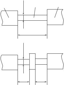
Touboul et al. [4] reported 1/f-noise measurements on two configurations of a Ni–Cr test film resistor with two Al film contacts, the films differing in length, as shown in Fig. 15. For each Ni–Cr film, let l, b, h, and n = l/b be the length, width, thickness, and aspect ratio, respectively. If the same current is passed through each resistor, volume power spectral densities SV1 and SV2 of the individual resistors are written
|
|
|
(a) |
|
|
|
|
Sc |
Sb |
1 |
Sc |
||
|
|
|
|
|
|
|
|
|
|
|
|
|
|
|
|
|
|
|
|
|
|
|
|
(b) |
|
|
|
|
Sc |
|
Sb |
|
|
Sc |
|
|
|
2 |
|
|
|
|
|
|
|
|
|
|
|
|
|
|
|
|
|
|
|
|
|
|
|
|
Fig. 15. Test film resistors used in an experiment on the extraction of contact noise from the total noise, the films differing in length [4].
|
|
(a) |
|
Cu |
b |
TaxNy |
Cu |
|
a1
(b)
b
SV1 = Sb1 + 2Sc , SV2 = Sb2 + 2Sc , |
(35) |
where Sc is the noise power spectral density of an individual contact and Sb1 and Sb2 are those of the two Ni−Cr films; furthermore, Sb1 = n 1Sb , Sb2 = n 2Sb ,
n 1 = l1/b1 , and n 2 = l2/b2 , where Sb is the noise of a square film with sides of length b [4].
Equations (35) enable one to find Sb1, Sb2 , Sc1, and Sc2 from measured SV1 and SV2. It is established that the noise of the film contacts is similar to 1/f noise; the level of the contact-pad noise depends on the current but not on the resistance of the Ni–Cr film [4]. However, the contact-pad noise has been found to account for less than 10% of the total resistor noise, a level that is difficult to measure [4].
Zhigal’skii and Karev [24] addressed the same problem in the context of test film resistors differing in length and in the number of film contacts, as shown in Fig. 16. The resistors share a substrate and have two or four film contacts. Note that their design allows one to use more film contacts.
Let SV1 and SV2 be the respective power spectral densities of 1/f noise from the two resistors, Sc be that of a film contact, b be the width of the resistive film, N1 and N2 be the respective numbers of film contacts on the two resistors, and Sb1 be the noise power spectral den-
a2 a2
Fig. 16. Test film resistors used in an experiment on the extraction of contact noise from the total noise, the films differing in length and the number of film contact joints [24].
sity for a square resistive film with sides of length b. We
also use this notation: n1 = a1/b, n2 = 2a2/b, t1 = N1/n1 , and t2 = N2/n2 . Let the current density be the same for
both resistors. If we assume that the respective excess noises of the resistor film and the contacts are uncorrelated, then
SV1 |
= N1Sc |
+ n1Sb1, |
|
(36) |
SV2 |
= N2Sc + n2Sb1. |
|
||
|
|
|||
Solving system (36) for Sc and Sb1 yields |
|
|||
Sc |
n1SV2n2SV1 |
|
(37) |
|
= ---------------------------- |
|
|
||
|
n1n2( t2 – t1 ) |
|
|
|
and |
|
|
|
|
|
N1SV2 |
– N2SV1 |
. |
(38) |
Sb1 = ----------------------------------- |
|
|||
|
n1n2( t1 – t2 ) |
|
|
|
JOURNAL OF COMMUNICATIONS TECHNOLOGY AND ELECTRONICS Vol. 50 No. 5 2005
496 |
ZHIGAL’SKII |
SE × 1016, Hz– 1 |
|
SN × 1012, Hz– 1 |
||
103 |
(a) |
|
103 |
(b) |
102 |
|
|
102 |
|
101 |
|
|
101 |
|
100 |
|
|
100 |
|
|
101 |
103 |
101 |
103 |
|
|
|
f, Hz |
|
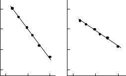
Fig. 17. Normalized power spectral densities of (a) equilib-
rium 1/f noise under dc driving and (b) nonequilibrium 1/f γ noise under pulsed test signal for TaxNy film resistors of
type 2 [24].
The contribution of film contacts to nonlinear behavior and 1/f noise is investigated most closely in the case of TaxNy thin films made by mass-production technology, using the configuration of Fig. 16 [24, 53, 69, 70]. The nonlinearity of the CVC was measured by secondand third-harmonic distortion [69] or by the dc component of a voltage response to pulsed driving [70], as in Section 3C.
Another line of research aims to identify the mechanism of nonequilibrium 1/f noise in TaxNy resistive films and Cu film contacts [24, 53, 69, 70] by considering the influence of process conditions on the noise. The resistive films were deposited on glass ceramic substrates by magnetron sputtering of a Ta target in a mixture of argon and nitrogen (10%) at different deposition rates [28]. The gas pressure was (7–10) × 10–2 Pa in all the cases. The deposition rate was varied via the
voltage at the target, the ion current Iion through the target being monitored. The substrate temperature was set
to 350°C.
The resistive films had a sheet resistance of 100 ± 10 Ω/ . The film contacts, 1 µm thick, were deposited on a Cr interlayer used to enhance adhesion. The metal films were produced by vacuum evaporation at a base pressure not greater than 7 × 10⁻⁴ Pa. Four types of thinfilm resistors were fabricated.
The resistors of types 1 and 2 differ in deposition rate. Type 1 is produced by a rapid process that lasts
6 min 40 s, with Iion = 1.5 A. For type 2, the deposition time is 52 min and Iion = 0.3 A.
The resistors of types 3 and 4 differ only in that with the latter the resistive film and film contacts are formed without breaking vacuum, the interval between the respective process stages being 3 min at most.
To reduce flicker noise, a resistive film of type 3 or 4 is made as a two-layer, in which the lower part is deposited at Iion = 1.2 A in 9 min and the higher part at
Iion = 0.3 A in 10 min [71]. A distinctive feature of the samples of type 4 was formation of both the resistive
layer and the contacts in one technological circuit without depressurizing the vacuum chamber, that is, the film deposition was followed within 3 min by the deposition of the chromium sublayer and then of the copper layer.
Once the film contacts are formed, resistors are subjected to vacuum annealing at 350°C for 30 min in order to stabilize the microstructure [72] and to reduce 1/f noise. Afterward, layers of Cu, Ni, and Au with thicknesses of 5, 0.5, and 2 µm, respectively, are electroplated serially on the film contacts.
The aspect ratios of the resistive films are n1 = 25 (Fig. 16a) and n2 = 10 (Fig. 16b). The other dimensions are a1 = 2500 µm, a2 = 500 µm, and b = 100 µm.
Nonequilibrium 1/f noise was examined in the frequency range 20–1000 Hz by measuring the power spectral density of fluctuations in Udc under pulsed current driving with a period of Tp = 8 µs and a length of τV1 = 1 µs having a different amplitude of Ip , the measurements being accurate to within 20% [24, 53]. In addition, noise power spectral density was measured under dc driving such that the voltage V0 across the resistor was equal to voltage-pulse height Vp under the pulsed test signal. A comparison was made between the results obtained in the two regimes.
For an individual film contact under dc driving at 6 mA, the noise power spectral density at 130 Hz varies with the resistor type as follows [24]:
Resistor type |
1 |
2 |
3 |
4 |
Sc × 1016, V2/Hz |
3500 |
Not available |
4 |
0.32 |
Notice that resistors of type 4 have a 1/f-noise level four orders of magnitude lower than that of type 1. Thus, the contribution of film contacts to the total noise is negligible only when the resistive film and film contacts are made without breaking vacuum (as with type 4).
The highest 1/f-noise level was observed in resistors made at a high deposition rate, the nonequilibrium flicker noise of the film contacts being as high as that of the film.
In general, the contribution of film contacts to the total 1/f noise may be much smaller than, comparable with, or larger than that of the resistive film, depending on fabrication conditions and rated resistance.
In resistors of type 2 (low deposition rate), the noise of the film contacts was much weaker than that of the film, and it was not possible to extract the noise by dc measurement. Pulsed test signal was used instead [24, 53]. Measurements of nonequilibrium 1/f noise obtained under pulsed test signal were compared with measurements of flicker noise under dc driving at V0 = Vp = 5 V (Fig. 17).
JOURNAL OF COMMUNICATIONS TECHNOLOGY AND ELECTRONICS Vol. 50 No. 5 2005