

AC and DC Parameters
7.19Boundary scan general timing
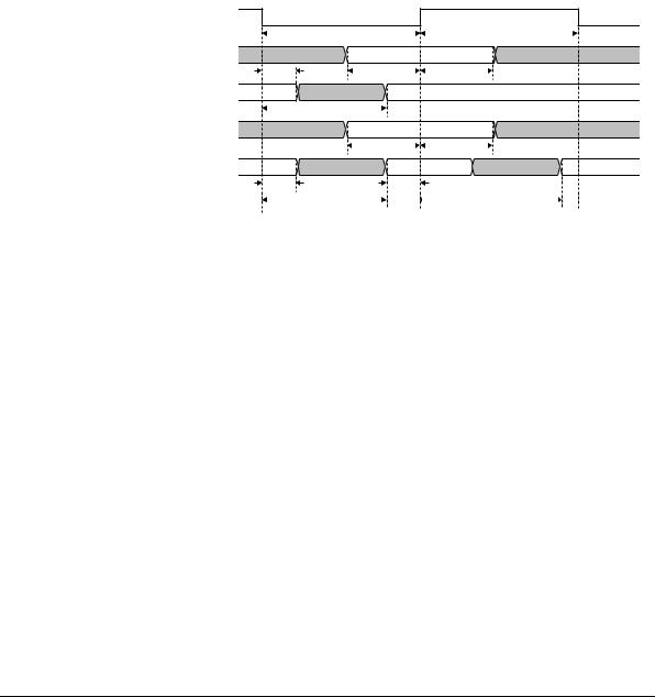
Figure 7-18 shows the ARM7TDMI processor boundary scan general timing. The timing parameters used in Figure 7-18 are listed in Table 7-18.
TCK
|
|
|
|
Tbscl |
|
|
|
|
|
|
|
|
|
|
|
|
|
|
|
|
Tbsch |
|
|
|
|
||||
TMS |
|
|
|
|
|
|
|
|
|
|
|
|
|
|
|
|
|
|
|
|
|||||||||
|
|
|
|
|
|
|
|
|
|
|
|
|
|
|
|
|
|
|
|
|
|
|
|
||||||
TDI |
|
|
|
|
|
|
|
|
|
|
|
|
|
|
|
|
|
|
|
|
|
|
|
||||||
|
|
|
|
|
|
|
|
|
|
|
|
|
|
|
|
|
|
|
|
|
|
|
|||||||
|
Tbsoh |
|
|
|
Tbsis |
|
|
|
|
|
Tbsih |
|
|
|
|
|
|
|
|
|
|||||||||
|
|
|
|
|
|
|
|
|
|
|
|
||||||||||||||||||
TDO |
|
|
|
|
|
|
|
|
|
|
|
|
|
|
|
|
|
|
|
|
|
|
|
||||||
|
|
|
|
|
|
|
|
|
|
|
|
|
|
|
|
|
|
|
|
|
|
|
|
|
|
|
|
|
|
|
|
|
Tbsod |
|
|
|
|
|
|
|
|
|
|
|
|
|
|
|
|
|
|
|
|
|
|
|
|
|
|
|
|
|
|
|
|
|
|
|
|
|
|
|
|
|
|
|
|
|
|
|
|
|
|
|
|
|
|||
Data in |
|
|
|
|
|
|
|
|
|
|
|
|
|
|
|
|
|
|
|
|
|
|
|
||||||
|
|
|
|
|
|
|
|
|
|
|
|
|
|
|
|
|
|
|
|
|
|
|
|
|
|
|
|
|
|
|
|
|
|
|
|
|
|
|
|
Tbsss |
|
|
|
|
|
|
Tbssh |
|
|
|
|
|
|
|
|
|
|||
Data out |
|
|
|
|
|
|
|
|
|
|
|||||||||||||||||||
|
|
|
|
|
|
|
|
|
|
|
|
|
|
|
|
|
|
|
|
|
|
|
|||||||
|
Tbsdh |
|
|
|
|
Tbsdh |
|
|
|
|
|
|
|
|
|
|
|
||||||||||||
|
|
|
Tbsdd |
|
|
|
|
|
|
|
|
|
|
|
|
|
|
|
|
|
Tbsdd |
|
|
|
|
||||
|
|
|
|
|
|
|
|
|
|
|
|
|
|
|
|
|
|
|
|
|
|
|
|||||||
|
|
|
|
|
|
|
|
|
|
|
Figure 7-18 Boundary scan general timing |
||||||||||||||||||
|
|
|
Table 7-18 Boundary scan general timing parameters |
||||||||||||||||||||||||||
|
|
|
|
|
|
|
|
|
|
|
|
|
|
|
|
|
|
|
|
|
|
|
|
|
|
|
|
|
|
|
|
Symbol |
|
Parameter |
|
|
|
|
|
|
|
|
Parameter type |
||||||||||||||||
|
|
|
|
|
|
|
|
|
|
|
|
|
|
|
|
|
|
|
|
|
|
|
|
|
|
|
|
|
|
|
|
Tbsch |
|
TCK high period |
Minimum |
||||||||||||||||||||||||
|
|
Tbscl |
|
TCK low period |
|
|
|
|
|
|
|
|
Minimum |
||||||||||||||||
|
|
Tbsdd |
|
TCK to data output valid |
Maximum |
||||||||||||||||||||||||
|
|
Tbsdh |
|
Data output hold time from TCK |
Minimum |
||||||||||||||||||||||||
|
|
Tbsih |
|
TDI, TMS hold from TCKr |
Minimum |
||||||||||||||||||||||||
|
|
Tbsis |
|
TDI, TMS setup to TCKr |
Minimum |
||||||||||||||||||||||||
|
|
Tbsod |
|
TCKf to TDO valid |
Maximum |
||||||||||||||||||||||||
|
|
Tbsoh |
|
TDO hold time from TCKf |
Minimum |
||||||||||||||||||||||||
|
|
Tbssh |
|
I/O signal setup from TCKr |
Minimum |
||||||||||||||||||||||||
|
|
Tbsss |
|
I/O signal setup to TCKr, |
Minimum |
||||||||||||||||||||||||
ARM DDI 0029G |
Copyright © 1994-2001. All rights reserved. |
7-23 |
AC and DC Parameters
7.20Reset period timing
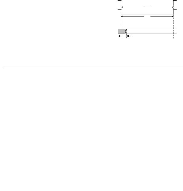
Figure 7-19 shows the ARM7TDMI reset period timing. The timing parameters used in Figure 7-19 are listed in Table 7-19.
nRESET
Trstl
nTRST
Tbsr
D[31:0]
DBGACK |
|
nCPI |
|
nENOUT |
|
nEXEC |
Trstd |
nMREQ |
|
SEQ |
|
Figure 7-19 Reset period timing
Table 7-19 Reset period timing parameters
Symbol |
Parameter |
Parameter type |
|
|
|
Tbsr |
nTRST reset period |
Minimum |
Trstd |
nRESETf to D[31:0], DBGACK, nCPI, nENOUT, nEXEC, nMREQ, SEQ valid |
Maximum |
Trstl |
nRESET LOW for guaranteed reset |
Minimum |
7-24 |
Copyright © 1994-2001. All rights reserved. |
ARM DDI 0029G |
AC and DC Parameters
7.21Output enable and disable times
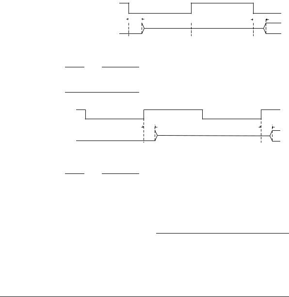
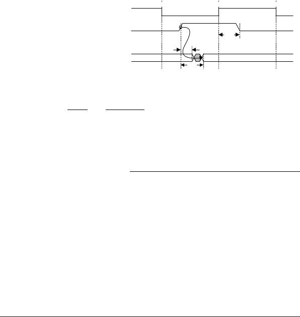
Figure 7-20 shows the output enable and disable times due to a HIGHZ TAP instruction. Figure 7-21 shows the output enable and disable times due to data scanning.The timing parameters used in Figure 7-20 and Figure 7-21 are listed in Table 7-20.
TCK
|
|
Tbsz |
|
|
|
|
Tbse |
|
|
|
|
||||
|
|
|
|
A[ ]
D[ ]
Figure 7-20 Output enable and disable times due to HIGHZ TAP instruction
Note
Figure 7-20 shows the Tbse, output enable time, parameter and Tbsz, output disable time, when the HIGHZ TAP instruction is loaded into the instruction register.
TCK
Tbsz |
Tbse |
A[ ]
D[ ]
Figure 7-21 Output enable and disable times due to data scanning
Note
Figure 7-21 shows the Tbse, output enable time, parameter and Tbsz, output disable time when data scanning, due to different logic levels being scanned through the scan cells for ABE and DBE.
Table 7-20 Output enable and disable timing parameters
Symbol |
Parameter |
Parameter type |
|
|
|
Tbse |
Output enable time |
Maximum |
Tbsz |
Output disable time |
Maximum |
ARM DDI 0029G |
Copyright © 1994-2001. All rights reserved. |
7-25 |
AC and DC Parameters
7.22Address latch enable control
Figure 7-22 shows the ARM7TDMI reset period timing. The timing parameters used in Figure 7-22 are listed in Table 7-21.
 Phase 1
 Phase 2

MCLK |
|
|
ALE |
|
|
|
Tald |
|
A[31:0] |
|
|
nRW |
Taleh |
|
LOCK |
||
|
||
nOPC |
Tale |
|
nTRANS |
MAS[1:0]
Figure 7-22 ALE control timing
Note
In Figure 7-22, Tald is the time by which ALE must be driven LOW to latch the current address in phase 2. If ALE is driven LOW after Tald, then a new address is latched. This is known as address breakthrough.
Table 7-21 ALE address control timing parameters
Symbol |
Parameter |
Parameter |
|
type |
|||
|
|
||
|
|
|
|
Tald |
Address group latch output time |
Maximum |
|
Tale |
Address group latch open output delay |
Maximum |
|
Taleh |
Address group latch output hold time |
Minimum |
7-26 |
Copyright © 1994-2001. All rights reserved. |
ARM DDI 0029G |