
- •Contents
- •List of Tables
- •List of Figures
- •Preface
- •About this document
- •Intended audience
- •Using this manual
- •Typographical conventions
- •Timing diagram conventions
- •Further reading
- •ARM publications
- •Other publications
- •Feedback
- •Feedback on the ARM7TDMI core
- •Feedback on this document
- •Introduction
- •1.1 About the ARM7TDMI core
- •1.1.1 The instruction pipeline
- •1.1.2 Memory access
- •1.1.3 Memory interface
- •1.1.4 EmbeddedICE Logic
- •1.2 Architecture
- •1.2.1 Instruction compression
- •1.2.2 The Thumb instruction set
- •1.3 Block, core, and functional diagrams
- •1.4 Instruction set summary
- •1.4.1 Format summary
- •1.4.2 ARM instruction summary
- •1.4.3 Thumb instruction summary
- •Programmer’s Model
- •2.1 About the programmer’s model
- •2.2 Processor operating states
- •2.2.1 Switching state
- •2.3 Memory formats
- •2.3.1 Little-endian
- •2.3.2 Big-Endian
- •2.4 Data types
- •2.5 Operating modes
- •2.6 Registers
- •2.6.4 Accessing high registers in Thumb state
- •2.7 The program status registers
- •2.7.1 Condition code flags
- •2.7.2 Control bits
- •2.7.3 Reserved bits
- •2.8 Exceptions
- •2.8.1 Exception entry and exit summary
- •2.8.2 Entering an exception
- •2.8.3 Leaving an exception
- •2.8.4 Fast interrupt request
- •2.8.5 Interrupt request
- •2.8.6 Abort
- •2.8.7 Software interrupt instruction
- •2.8.8 Undefined instruction
- •2.8.9 Exception vectors
- •2.8.10 Exception priorities
- •2.9 Interrupt latencies
- •2.9.1 Maximum interrupt latencies
- •2.9.2 Minimum interrupt latencies
- •2.10 Reset
- •Memory Interface
- •3.1 About the memory interface
- •3.2 Bus interface signals
- •3.3 Bus cycle types
- •3.3.1 Nonsequential cycles
- •3.3.2 Sequential cycles
- •3.3.3 Internal cycles
- •3.3.4 Merged IS cycles
- •3.3.5 Coprocessor register transfer cycles
- •3.3.6 Summary of ARM memory cycle timing
- •3.4 Addressing signals
- •3.4.4 nOPC
- •3.4.5 nTRANS
- •3.4.6 LOCK
- •3.4.7 TBIT
- •3.5 Address timing
- •3.6 Data timed signals
- •3.6.1 D[31:0], DOUT[31:0], and DIN[31:0]
- •3.6.2 ABORT
- •3.6.3 Byte latch enables
- •3.6.4 Byte and halfword accesses
- •3.7 Stretching access times
- •3.7.1 Modulating MCLK
- •3.7.2 Use of nWAIT to control bus cycles
- •3.8 Action of ARM7TDMI core in debug state
- •3.9 Privileged mode access
- •3.10 Reset sequence after power up
- •Coprocessor Interface
- •4.1 About coprocessors
- •4.1.1 Coprocessor availability
- •4.2 Coprocessor interface signals
- •4.3 Pipeline following signals
- •4.4 Coprocessor interface handshaking
- •4.4.1 The coprocessor
- •4.4.2 The ARM7TDMI processor
- •4.4.3 Coprocessor signaling
- •4.4.5 Coprocessor register transfer instructions
- •4.4.6 Coprocessor data operations
- •4.4.7 Coprocessor load and store operations
- •4.5 Connecting coprocessors
- •4.5.1 Connecting a single coprocessor
- •4.5.2 Connecting multiple coprocessors
- •4.6 If you are not using an external coprocessor
- •4.7 Undefined instructions
- •4.8 Privileged instructions
- •Debug Interface
- •5.1 About the debug interface
- •5.1.1 Stages of debug
- •5.1.2 Clocks
- •5.2 Debug systems
- •5.2.1 Debug host
- •5.2.2 Protocol converter
- •5.2.3 Debug target
- •5.3 Debug interface signals
- •5.3.1 Entry into debug state
- •5.3.2 Action of the processor in debug state
- •5.4 ARM7TDMI core clock domains
- •5.4.1 Clock switch during debug
- •5.4.2 Clock switch during test
- •5.5 Determining the core and system state
- •5.6 About EmbeddedICE Logic
- •5.7 Disabling EmbeddedICE
- •5.8 Debug Communications Channel
- •5.8.1 DCC registers
- •5.8.2 Communications through the DCC
- •Instruction Cycle Timings
- •6.1 About the instruction cycle timing tables
- •6.2 Branch and branch with link
- •6.3 Thumb branch with link
- •6.4 Branch and Exchange
- •6.5 Data operations
- •6.6 Multiply and multiply accumulate
- •6.7 Load register
- •6.8 Store register
- •6.9 Load multiple registers
- •6.10 Store multiple registers
- •6.11 Data swap
- •6.12 Software interrupt and exception entry
- •6.13 Coprocessor data operation
- •6.14 Coprocessor data transfer from memory to coprocessor
- •6.15 Coprocessor data transfer from coprocessor to memory
- •6.16 Coprocessor register transfer, load from coprocessor
- •6.17 Coprocessor register transfer, store to coprocessor
- •6.18 Undefined instructions and coprocessor absent
- •6.19 Unexecuted instructions
- •6.20 Instruction speed summary
- •AC and DC Parameters
- •7.1 Timing diagram information
- •7.2 General timing
- •7.3 Address bus enable control
- •7.4 Bidirectional data write cycle
- •7.5 Bidirectional data read cycle
- •7.6 Data bus control
- •7.8 Unidirectional data write cycle timing
- •7.9 Unidirectional data read cycle timing
- •7.10 Configuration pin timing
- •7.11 Coprocessor timing
- •7.12 Exception timing
- •7.13 Synchronous interrupt timing
- •7.14 Debug timing
- •7.15 Debug communications channel output timing
- •7.16 Breakpoint timing
- •7.17 Test clock and external clock timing
- •7.18 Memory clock timing
- •7.19 Boundary scan general timing
- •7.20 Reset period timing
- •7.21 Output enable and disable times
- •7.22 Address latch enable control
- •7.23 Address pipeline control timing
- •7.24 Notes on AC Parameters
- •7.25 DC parameters
- •Signal Description
- •A.1 Signal description
- •A.1.1 Transistor dimensions
- •A.1.2 Signal types
- •A.1.3 Signals
- •Debug in Depth
- •B.1 Scan chains and JTAG interface
- •B.1.1 Scan chain implementation
- •B.1.2 TAP state machine
- •B.2 Resetting the TAP controller
- •B.3 Pullup resistors
- •B.4 Instruction register
- •B.5 Public instructions
- •B.5.1 EXTEST (0000)
- •B.5.2 SCAN_N (0010)
- •B.5.3 SAMPLE/PRELOAD (0011)
- •B.5.4 RESTART (0100)
- •B.5.5 CLAMP (0101)
- •B.5.6 HIGHZ (0111)
- •B.5.7 CLAMPZ (1001)
- •B.5.8 INTEST (1100)
- •B.5.9 IDCODE (1110)
- •B.5.10 BYPASS (1111)
- •B.6 Test data registers
- •B.6.1 Bypass register
- •B.6.2 ARM7TDMI core device IDentification (ID) code register
- •B.6.5 Scan chains 0, 1, 2, and 3
- •B.7 The ARM7TDMI core clocks
- •B.7.1 Clock switch during debug
- •B.7.2 Clock switch during test
- •B.8 Determining the core and system state
- •B.8.1 Determining the core state
- •B.8.2 Determining system state
- •B.8.3 Exit from debug state
- •B.9 Behavior of the program counter during debug
- •B.9.1 Breakpoints
- •B.9.2 Watchpoints
- •B.9.3 Watchpoint with another exception
- •B.9.4 Debug request
- •B.9.5 System speed access
- •B.9.6 Summary of return address calculations
- •B.10 Priorities and exceptions
- •B.10.1 Breakpoint with Prefetch Abort
- •B.10.2 Interrupts
- •B.10.3 Data Aborts
- •B.11 Scan chain cell data
- •B.11.1 Scan chain 0 cells
- •B.11.2 Scan chain 1 cells
- •B.12 The watchpoint registers
- •B.12.1 Programming and reading watchpoint registers
- •B.12.2 Using the mask registers
- •B.12.3 The control registers
- •B.13 Programming breakpoints
- •B.13.1 Hardware breakpoints
- •B.13.2 Software breakpoints
- •B.14 Programming watchpoints
- •B.15 The debug control register
- •B.16 The debug status register
- •B.17 Coupling breakpoints and watchpoints
- •B.17.1 Breakpoint and watchpoint coupling example
- •B.17.2 RANGEOUT signal
- •B.18 EmbeddedICE timing
- •B.19 Programming Restriction
- •Glossary
- •Index

AC and DC Parameters
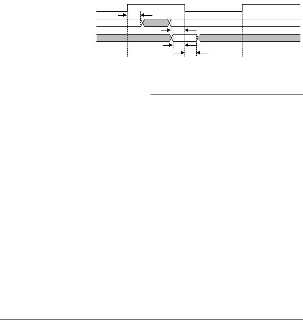
7.8Unidirectional data write cycle timing
Figure 7-7 shows the ARM7TDMI processor unidirectional data write cycle timing. The timing parameters used in Figure 7-6 on page 7-10 are listed in Table 7-6 on page 7-10.
MCLK
Tnen
nENOUT
Tdohu
DOUT[31:0]
Tdoutu
Figure 7-7 Unidirectional data write cycle timing
Table 7-7 Unidirectional data write cycle timing parameters
Symbol |
Parameter |
Parameter type |
|
|
|
Tdohu |
DOUT[31:0] hold time from MCLKf |
Minimum |
Tdoutu |
MCLKf to DOUT[31:0] valid |
Maximum |
Tnen |
MCLKf to nENOUT valid |
Maximum |
ARM DDI 0029G |
Copyright © 1994-2001. All rights reserved. |
7-11 |

AC and DC Parameters
7.9Unidirectional data read cycle timing
Figure 7-8 shows the ARM7TDMI processor unidirectional data read cycle timing. The timing parameters used in Figure 7-7 on page 7-11 are listed in Table 7-7 on page 7-11.
MCLK
nENOUT
|
Tnen |
|
|
|
|
|
|
|
Tdisu |
|
|
|
|
||||||
|
|
|
|
|
|
|
|
|
|
DIN[31:0]
Tdihu
BL[3:0]
Tbylh
Tbyls
Figure 7-8 Unidirectional data read cycle timing
Table 7-8 Unidirectional data read cycle timing parameters
Symbol |
Parameter |
Parameter type |
|
|
|
Tbylh |
BL[3:0] hold time from MCLKf |
Minimum |
Tbyls |
BL[3:0] set up to from MCLKr |
Minimum |
Tdihu |
DIN[31:0] hold time from MCLKf |
Minimum |
Tdisu |
DIN[31:0] set up time to MCLKf |
Minimum |
Tnen |
MCLKf to nENOUT valid |
Maximum |
7-12 |
Copyright © 1994-2001. All rights reserved. |
ARM DDI 0029G |

AC and DC Parameters
7.10Configuration pin timing
Figure 7-9 shows the ARM7TDMI processor configuration pin timing. The timing parameters used in Figure 7-9 are listed in Table 7-9.
MCLK
Tcth
BIGEND
Tcts
ISYNC
Tcts
Tcth
Figure 7-9 Configuration pin timing
Table 7-9 Configuration pin timing parameters
Symbol |
Parameter |
Parameter type |
|
|
|
Tcth |
Configurations hold time |
Minimum |
Tcts |
Configuration setup time |
Minimum |
ARM DDI 0029G |
Copyright © 1994-2001. All rights reserved. |
7-13 |

AC and DC Parameters
7.11Coprocessor timing
Figure 7-10 shows the ARM7TDMI processor coprocessor timing. The timing parameters used in Figure 7-10 are listed in Table 7-10.
Phase 1 |
Phase 2 |
|
MCLK |
|
|
Tcpi |
Tcpih |
|
nCPI |
|
|
CPA |
Tcps |
|
|
||
CPB |
Tcph |
|
nMREQ |
||
|
||
SEQ |
|
Tcpms
Figure 7-10 Coprocessor timing
Note
In Figure 7-10, usually nMREQ and SEQ become valid Tmsd after the falling edge of MCLK. In this cycle the core has been busy-waiting for a coprocessor to complete the instruction. If CPA and CPB change during phase 1, the timing of nMREQ and SEQ depends on Tcpms. Most systems can generate CPA and CPB during the previous phase 2, and so the timing of nMREQ and SEQ is always Tmsd.
Table 7-10 Coprocessor timing parameters
Symbol |
Parameter |
Parameter type |
|
|
|
Tcph |
CPA,CPB hold time from MCLKr |
Minimum |
Tcpi |
MCLKf to nCPI valid |
Maximum |
Tcpih |
nCPI hold time from MCLKf |
Minimum |
Tcpms |
CPA, CPB to nMREQ, SEQ |
Maximum |
Tcps |
CPA, CPB setup to MCLKr |
Minimum |
7-14 |
Copyright © 1994-2001. All rights reserved. |
ARM DDI 0029G |