

Memory Interface
3.6Data timed signals
This section describes:
•D[31:0], DOUT[31:0], and DIN[31:0]
•ABORT on page 3-24
•Byte latch enables on page 3-24
•Byte and halfword accesses on page 3-26.
3.6.1D[31:0], DOUT[31:0], and DIN[31:0]
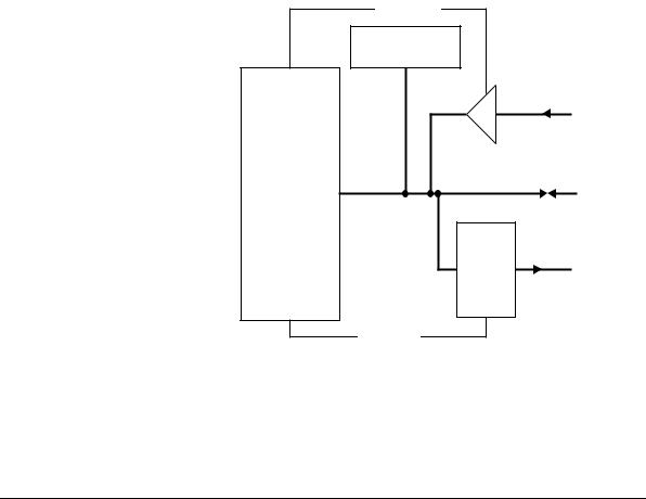
The ARM7TDMI processor provides both unidirectional data buses, DIN[31:0], DOUT[31:0], and a bidirectional data bus, D[31:0]. The configuration input BUSEN is used to select which is active. Figure 3-11 shows the arrangement of the data buses and bus-splitter logic.
Buffer control
EmbeddICE |
|
Logic |
|
|
DIN[31:0] |
ARM7TDMI |
D[31:0] |
Latch |
DOUT[31:0] |
G |
|
Latch control
Figure 3-11 External bus arrangement
When the bidirectional data bus is being used then you must disable the unidirectional buses by driving BUSEN LOW. The timing of the bus for three cycles, load-store-load, is shown in Figure 3-12 on page 3-18.
ARM DDI 0029G |
Copyright © 1994-2001. All rights reserved. |
3-17 |

Memory Interface
read cycle write cycle read cycle
MCLK
D[31:0]
Figure 3-12 Bidirectional bus timing
Unidirectional data bus
When BUSEN is HIGH, all instructions and input data are presented on the input data bus, DIN[31:0]. The timing of this data is similar to that of the bidirectional bus when in input mode. Data must be set up and held to the falling edge of MCLK. For the exact timing requirements refer to Chapter 7 AC and DC Parameters.
In this configuration, all output data is presented on DOUT[31:0]. The value on this bus only changes when the processor performs a store cycle. Again, the timing of the data is similar to that of the bidirectional data bus. The value on DOUT[31:0] changes after the falling edge of MCLK.
The bus timing of a read-write-read cycle combination is shown in Figure 3-13.
|
read cycle |
write cycle |
read cycle |
MCLK |
|
|
|
DIN[31:0] |
D1 |
|
D2 |
DOUT[31:0] |
|
|
Dout |
D[31:0] |
D1 |
Dout |
D2 |
Figure 3-13 Unidirectional bus timing
When the unidirectional data buses are being used, and BUSEN is HIGH, the bidirectional bus, D[31:0], must be left unconnected.
The unidirectional buses are typically used internally in ASIC embedded applications. Externally, most systems still require a bidirectional data bus to interface to external memory. Figure 3-14 on page 3-19 shows how you can join the unidirectional buses up at the pads of an ASIC to connect to an external bidirectional bus.
3-18 |
Copyright © 1994-2001. All rights reserved. |
ARM DDI 0029G |

Memory Interface
nENOUT
PAD
DOUT[31:0]
XDATA[31:0]
ARM7TDMI
DIN[31:0]
Figure 3-14 External connection of unidirectional buses
Bidirectional data bus
When BUSEN is LOW, the buffer between DIN[31:0] and D[31:0] is disabled. Any data presented on DIN[31:0] is ignored. Also, when BUSEN is LOW, the value on DOUT[31:0] is forced to 0x00000000.
When the ARM7TDMI processor is reading from memory DIN[31:0] is acting as an input. During write cycles the ARM7TDMI core must output data. During phase 2 of the previous cycle, the signal nRW is driven HIGH to indicate a write cycle. During the actual cycle, nENOUT is driven LOW to indicate that the processor is driving D[31:0] as an output. Figure 3-15 on page 3-20 shows the bus timing with the data bus enabled. Figure 3-16 on page 3-20 shows the circuit that exists in the processor for controlling exactly when the external bus is driven out.
ARM DDI 0029G |
Copyright © 1994-2001. All rights reserved. |
3-19 |
Memory Interface
 memory cycle

MCLK
A[31:0] 

nRW
nENOUT
D[31:0]
Figure 3-15 Data write bus cycle
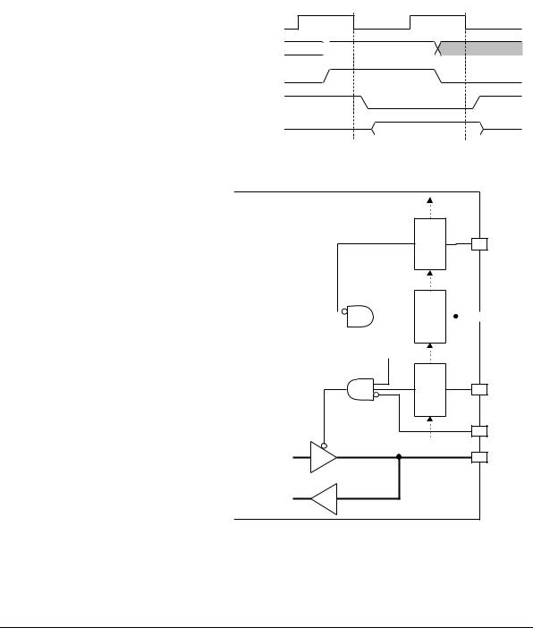
ARM7TDMI
scan
DBE
cell
data direction |
|
|
|
|
scan |
|
|
|
nENOUT |
|||
control from |
|
|
|
|
|
cell |
|
|
|
|
|
|
|
|
|
||||||||||
core |
|
|
|
|
|
|
|
|
|
|||
|
|
|
|
|
|
|
|
|
|
|
|
|
scan
nENIN
cell
TBE
write data
D[31:0]
from core
read data to core
Figure 3-16 Data bus control circuit
3-20 |
Copyright © 1994-2001. All rights reserved. |
ARM DDI 0029G |
Memory Interface
The macrocell has an additional bus control signal, nENIN that allows the external system to manually tristate the bus. In the simplest systems, nENIN can be tied LOW and nENOUT can be ignored. In many applications, when the external data bus is a shared resource, greater control might be required. In this situation, nENIN can be used to delay when the external bus is driven.
Note
For backwards compatibility, DBE is also included. At the macrocell level, DBE and nENIN have almost identical functionality and in most applications one can be tied to keep the data bus enabled.
The processor has another output control signal called TBE. This signal is usually only used during test and must be tied HIGH when not in use. When driven LOW, TBE forces all tristateable outputs to high impedance, it is as though both DBE and ABE have been driven LOW, causing the data bus, the address bus, and all other signals normally controlled by ABE to become high impedance.
Note
There is no scan cell on TBE. Therefore, TBE is completely independent of scan data and can be used to put the outputs into a high impedance state while scan testing takes place.
Table 3-6 lists the tristate control of the processor outputs.
Table 3-6 Tristate control of processor outputs
Processor output |
ABE |
DBE |
TBE |
|
|
|
|
A[31:0] |
Yes |
- |
Yes |
|
|
|
|
D[31:0] |
- |
Yes |
Yes |
|
|
|
|
nRW |
Yes |
- |
Yes |
|
|
|
|
LOCK |
Yes |
- |
Yes |
|
|
|
|
MAS[1:0] |
Yes |
- |
Yes |
|
|
|
|
nOPC |
Yes |
- |
Yes |
|
|
|
|
nTRANS |
Yes |
- |
Yes |
|
|
|
|
ARM DDI 0029G |
Copyright © 1994-2001. All rights reserved. |
3-21 |

Memory Interface
ARM7TDMI core test chip example system
Connecting the ARM7TDMI processor data bus, D[31:0] to an external shared bus requires additional logic that varies between applications in the case of a test chip.
In this application, care must be taken to prevent bus clash on D[31:0] when the data bus drive changes direction. The timing of nENIN, and the pad control signals must be arranged so that when the core starts to drive out, the pad drive onto D[31:0] is disabled before the core starts to drive. Similarly, when the bus switches back to input, the core must stop driving before the pad is enabled.
The circuit implemented in the ARM7TDMI processor test chip is shown in Figure 3-17 on page 3-23.
3-22 |
Copyright © 1994-2001. All rights reserved. |
ARM DDI 0029G |

Memory Interface
ARM7TDMI test chip or product
ARM7TDMI core
MCLK
|
|
|
MCLK |
|
|
Vdd |
|
scan |
DBE |
|
nEDBE |
cell |
|
|
EDBE |
|
|
|
|
|
|
|
nEN2 |
scan |
nENOUT |
|
|
cell |
|
|
|
scan |
nENIN |
|
nEN1 |
cell |
|
|
|
|
|
|
|
|
Vdd |
Vss |
Pad |
|
|
|
|
|
TBE |
|
|
|
|
|
XD[31:0] |
|
D[31:0] |
|
|
Figure 3-17 Test chip data bus circuit
Note
At the core level, TBE and DBE are inactive, tied HIGH, because in a packaged part you do not have to manually force the internal buses into a high impedance state. At the pad level, the test chip signal EDBE is used by the bus control logic to allow the external memory controller to arbitrate the bus and asynchronously disable the ARM7TDMI core test chip if necessary.
ARM DDI 0029G |
Copyright © 1994-2001. All rights reserved. |
3-23 |