

chapter7_pub.fm Page 310 Wednesday, November 22, 2000 8:41 AM
310 |
DESIGNING SEQUENTIAL LOGIC CIRCUITS |
Chapter 7 |
notorious example is the address transition detection (ATD) circuit, used for the timing generation in static memories. This circuit detects a change in a signal, or group of signals, such as the address or data bus, and produces a pulse to initialize the subsequent circuitry.
The most common approach to the implementation of one-shots is the use of a simple delay element to control the duration of the pulse. The concept is illustrated in Figure 7.51. In the quiescent state, both inputs to the XOR are identical, and the output is low. A transition on the input causes the XOR inputs to differ temporarily and the output to go high. After a delay td (of the delay element), this disruption is removed, and the output goes low again. A pulse of length td is created. The delay circuit can be realized in many different ways, such as an RC-network or a chain of basic gates.
In |
|
|
DELAY |
Out |
|
td |
||
t |
||
|
d |
|
Figure 7.51 Transition-triggered one-shot. |
|
7.9.3Astable Circuits
An astable circuit has no stable states. The output oscillates back and forth between two quasi-stable states with a period determined by the circuit topology and parameters (delay, power supply, etc.). One of the main applications of oscillators is the on-chip generation of clock signals. This application is discussed in detail in a later chapter (on timing).
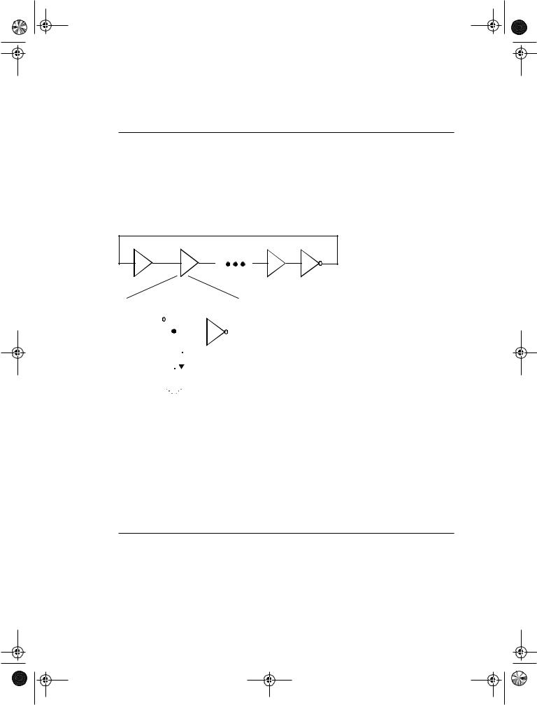
The ring oscillator is a simple, example of an astable circuit. It consists of an odd number of inverters connected in a circular chain. Due to the odd number of inversions, no stable operation point exists, and the circuit oscillates with a period equal to 2 × tp × N, with N the number of inverters in the chain and tp the propagation delay of each inverter.
Example 7.8 Ring oscillator
The simulated response of a ring oscillator with five stages is shown in Figure 7.52 (all gates use minimum-size devices). The observed oscillation period approximately equals 0.5 nsec, which corresponds to a gate propagation delay of 50 psec. By tapping the chain at various points, different phases of the oscillating waveform are obtained (phases 1, 3, and 5 are dis-
Volts
3.0 |
|
v1 v3 v5 |
|
|
|
|
|
||
|
|
|
|
|
2.5 |
|
|
|
|
2.0 |
|
|
|
|
1.5 |
|
|
|
|
1.0 |
|
|
|
|
0.5 |
|
|
|
|
0.0 |
|
|
|
Figure 7.52 Simulated |
|
|
|
waveforms of five-stage ring |
|
|
|
|
|
|
-0.5 |
|
|
|
oscillator. The outputs of stages 1, |
|
|
|||
|
|
|
|
0.0 |
0.5 |
1.0 |
1.5 |
3, and 5 are shown. |
|
|
time (nsec) |
|
|
chapter7_pub.fm Page 311 Wednesday, November 22, 2000 8:41 AM
Section 7.9 |
Non-Bistable Sequential Circuits |
311 |
played in the plot). A wide range of clock signals with different duty-cycles and phases can be derived from those elementary signals using simple logic operations.
The ring oscillator composed of cascaded inverters produces a waveform with a fixed oscillating frequency determined by the delay of an inverter in the CMOS process. In many applications, it is necessary to control the frequency of the oscillator. An example of such a circuit is the voltage-controlled oscillator (VCO), whose oscillation frequency is a function (typically non-linear) of a control voltage. The standard ring oscillator can be modified into a VCO by replacing the standard inverter with a current-starved inverter as shown in Figure 7.53 [Jeong87]. The mechanism for controlling the delay of each inverter is to limit the current available to discharge the load capacitance of the gate.
|
|
|
|
|
VDD |
|
|
|
|
|
|||||
|
|
|
|
|
|
|
|
|
|
|
|
|
|
|
|
|
|
|
|
|
|
|
|
|
|
|
|
|
|
|
|
In |
|
|
|
|
M2 |
|
|
Out |
|
||||||
|
|
|
|
|
|
|
|||||||||
|
|
|
|
|
|
|
|
|
|
||||||
|
|
|
|
|
|
|
|
|
|
|
|
|
|
|
|
|
|
|
|
|
|
|
|
|
|
|
|
|
|
|
|
|
|
|
|
|
|
M1 |
Iref |
|
|||||||
|
|
|
|
|
|
|
|||||||||
|
|
|
|
|
|
|
|
|
|
|
|
||||
|
|
|
|
|
|
|
|
|
|
|
|
||||
|
|
|
|
|
|
|
|
|
|
|
|
||||
|
|
|
|
|
|
M3 |
|
|
|
Figure 7.53 |
Voltage-controlled oscillator based on |
||||
|
|
Vcntl |
|
|
|
|
current-starved inverters. |
||||||||
|
|
|
|
|
|
|
|
|
|
|
|||||
|
|
|
|
|
|
|
|
|
|
|
|
|
|
|
|
|
|
|
|
|
|
|
|
|
|
|
|
|
|
|
|
In this modified inverter circuit, the maximal discharge current of the inverter is limited by adding an extra series device. Note that the low-to-high transition on the inverter can also be controlled by adding a PMOS device in series with M2. The added NMOS transistor M3, is controlled by an analog control voltage Vcntl, which determines the available discharge current. Lowering Vcntl reduces the discharge current and, hence, increases tpHL. The ability to alter the propagation delay per stage allows us to control the frequency of the ring structure. The control voltage is generally set using feedback techniques. Under low operating current levels, the current-starved inverter suffers from slow fall times at its output. This can result in significant short-circuit current. This is resolved by feeding its output into a CMOS inverter or better yet a Schmitt trigger. An extra inverter is needed at the end to ensure that the structure oscillates.
Example 7.9 Current-Starved Inverter Simulation
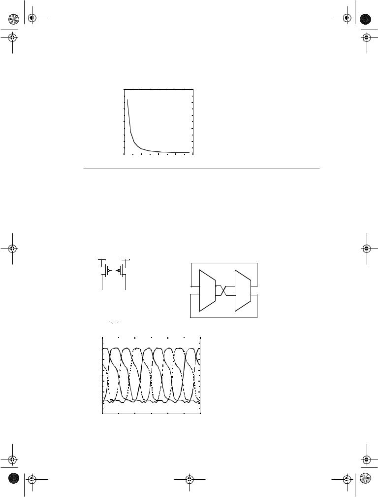
Figure 7.54 show the simulated delay of the current-starved inverter as a function of the con-
trol voltage Vcntl. The delay of the inverter can be varied over a large range. When the control voltage is smaller than the threshold, the device enters the sub-threshold region. This results
in large variations of the propagation delay, as the drive current is exponentially dependent on the drive voltage. When operating in this region, the delay is very sensitive to variations in the control voltage, and, hence, to noise.
chapter7_pub.fm Page 312 Wednesday, November 22, 2000 8:41 AM
312 |
DESIGNING SEQUENTIAL LOGIC CIRCUITS |
Chapter 7 |
tpHL (nsec)
5.0 
4.0 
3.0 
2.0 
|
|
|
|
|
|
Figure 7.54 tpHL of current-starved |
1.0 |
|
|
|
|
|
inverter as a function of the control |
|
|
|
|
|
|
voltage. |
0.0 |
|
|
|
|
|
|
|
1.0 |
1.5 |
2.0 |
2.5 |
||
0.5 |
||||||
Vctrl (V)
Another approach to implement the delay element is to use a differential element as shown in Figure 7.55a. Since the delay cell provides both inverting and non-inverting outputs, an oscillator with an even number of stages can be implemented. Figure 7.55b shows a two-stage differential VCO, where the feedback loop provides 180o phase shift through two gate delays, one non-inverting and the other inverting, therefore forming an oscillation. The simulated waveforms of this two stage VCO are shown in Figure 7.55c. The inphase and quadrature phase outputs are available simultaneously. The differential type VCO has better immunity to common mode noise (for example, supply noise) compared to the common ring oscillator. However, it consumes more power due to the increased complexity, and the static current.
Vo- 
 Vo+
Vo+
in+ |
|
|
|
|
|
|
|
|
|
|
|
|
|
in- |
|
|
|
|
|
|
|
|
|
|
|
|
|
||
|
|
|
|
|
|
|
|
|
|
|
|
|
||
|
|
|
|
|
|
|
|
|
|
|
|
|
|
|
|
|
|
|
|
|
|
|
|
|
|
|
|
|
|
|
Vctrl |
|
|
|
|
|
|
|
|
|
|
|||
|
|
|
|
|
|
|
|
|
|
|
||||
|
|
|
|
|
|
|
|
|
|
|
||||
|
|
|
|
|
|
|
|
|
|
|
|
|
|
|
v1 |
i+ o+ |
v3 |
i+ o+ |
||
|
|||||
v2 |
i- |
o- |
v4 |
i- |
o- |
|
|
|
|
|
|
Volts
(a) delay cell |
|
(b) two stage VCO |
||
3.0 |
|
|
|
|
v1 v2 v3 |
v4 |
|||
2.5 |
||||
|
|
|
||
2.0 |
|
|
|
|
1.5 |
|
|
|
|
1.0 |
|
|
|
|
0.5 |
|
|
|
|
0.0 |
|
|
|
|
-0.5 |
|
|
Figure 7.55 Differential delay |
|
0.5 |
1.5time (nsec)2.5 |
3.5 |
||
element and VCO topology. |
||||
|
|
|
(c) simulated waveforms of 2-stage VCO

chapter7_pub.fm Page 313 Wednesday, November 22, 2000 8:41 AM
Section 7.10 |
Perspective: Choosing a Clocking Strategy |
313 |
7.10Perspective: Choosing a Clocking Strategy
A crucial decision that must be made in the earliest phases of a chip design is to select the appropriate clocking methodology. The reliable synchronization of the various operations occurring in a complex circuit is one of the most intriguing challenges facing the digital designer of the next decade. Choosing the right clocking scheme affects the functionality, speed and power of a circuit.
A number of widely-used clocking schemes were introduced in this chapter. The most robust and conceptually simple scheme is the two-phase master-slave design. The predominant approach is use the multiplexer-based register, and to generate the two clock phases locally by simply inverting the clock. More exotic schemes such as the glitch register are also used in practice. However, these schemes require significant hand tuning and must only be used in specific situations. An example of such is the need for a negative setup time to cope with clock skew.
The general trend in high-performance CMOS VLSI design is therefore to use simple clocking schemes, even at the expense of performance. Most automated design methodologies such as standard cell employ a single-phase, edge-triggered approach, based on static flip-flops. But the tendency towards simpler clocking approaches is also apparent in high-performance designs such as microprocessors. The use of latches between logic is also very common to improve circuit performance.
7.11Summary
This chapter has explored the subject of sequential digital circuits. The following topics were discussed:
•The cross-coupling of two inverters creates a bistable circuit, called a flip-flop. A third potential operation point turns out to be metastable; that is, any diversion from this bias point causes the flip-flop to converge to one of the stable states.
•A latch is a level-sensitive memory element that samples data on one phase and holds data on the other phase. A register (sometime also called a flip-flop) on the other hand samples the data on the rising or falling edge. A register has three important parameter the set-up time, the hold time, and the propagation delay. These parameters must be carefully optimized since they may account for a significant portion of the clock period.
•Registers can be static or dynamic. A static register holds state as long as the power supply is turned on. It is ideal for memory that is accessed infrequently (e.g., reconfiguration registers or control information). Dynamic memory is based on temporary charge store on capacitors. The primary advantage is the reduced complexity and higher performance/lower power. However, charge on a dynamic node leaks away with time, and hence dynamic circuits have a minimum clock frequency.
•There are several fundamentally different approaches towards building a register. The most common and widely used approach is the master-slave configuration which involves cascading a positive latch and negative latch (or vice-versa).

chapter7_pub.fm Page 314 Wednesday, November 22, 2000 8:41 AM
314 |
DESIGNING SEQUENTIAL LOGIC CIRCUITS |
Chapter 7 |
•Registers can also be constructed using the pulse or glitch concept. An intentional pulse (using a one shot circuit) is used to sample the input around an edge. Generally, the design of such circuits requires careful timing analysis across all process corners. Sense-amplifier based schemes are also used to construct registers and are to be used when high performance or low signal swing signalling is required.
•Choice of clocking style is an important consideration. Two phase design can result in race problems. Circuit techniques such as C2MOS can be used to eliminate race
conditions in two-phase clocking. Another option is to use true single phase clocking. However, the rise time of clocks must be carefully optimized to eliminate races.
•The combination of dynamic logic with dynamic latches can produce extremely fast computational structures. An example of such an approach, the NORA logic style, is very effective in pipelined datapaths.
•Monostable structures have only one stable state. They are useful as pulse generators.
•Astable multivibrators, or oscillators, possess no stable state. The ring oscillator is the best-known example of a circuit of this class.
•Schmitt triggers display hysteresis in their dc characteristic and fast transitions in their transient response. They are mainly used to suppress noise.
7.12To Probe Further
The basic concepts of sequential gates can be found in many logic design textbooks (e.g., [Mano82] and [Hill74]). The design of sequential circuits is amply documented in most of the traditional digital circuit handbooks.
References
[Dopperpuhl92] D. Dopperpuhl et al., “A 200 MHz 64-b Dual Issue CMOS Microprocessor,” IEEE JSSC, vol. 27, no. 11, Nov. 1992, pp. 1555–1567.
[Gieseke97] B. Bieseke et al., “A 600MHz Superscalar RISC Microprocessor with Out-Of-Order Execution,” IEEE ISSCC, pp. 176-177, Feb. 1997.
[Goncalves83] N. Goncalves and H. De Man, “NORA: a racefree dynamic CMOS technique for pipelined logic structures,” IEEE JSSC, vol. SC-18, no. 3, June 1983, pp. 261–266.
[Haznedar91] H. Haznedar, Digital Microelectronics, Benjamin/Cummings, 1991.
[Hill74] F. Hill and G. Peterson, Introduction to Switching Theory and Logical Design, Wiley, 1974.
[Hodges88] D. Hodges and H. Jackson, Analysis and Design of Digital Integrated Circuits, McGraw-Hill, 1988.
[Jeong87] D. Jeong et al., “Design of PLL-based clock generation circuits,” IEEE JSSC, vol. SC-22, no. 2, April 1987, pp. 255–261.
[Kuzo96] S. Kuzo et al., “A 100MHz 0.4W RISC Processor with 200MHz Multiply-Adder, using Pulse-Register Technique,” IEEE ISSCC, pp. 140-141, February 1996.
[Mano82] M. Mano, Computer System Architecture, Prentice Hall, 1982.
[Montanaro96] J. Montanaro et al., “A 160-MHz, 32-b, 0.5-W CMOS RISC Microprocessor,” IEEE JSSC, pp. 1703-1714, November 1996.
chapter7_pub.fm Page 315 Wednesday, November 22, 2000 8:41 AM
Section 7.12 |
To Probe Further |
315 |
[Mutoh95] S. Mutoh et al., “1-V Power Supply High-Speed Digital Circuit Technology with Multi- threshold-Voltage CMOS,” IEEE JSSC , pp. 847-854, August 1995.
[Partovi96] H. Partovi, “Flow-Through Latch and Edge-Triggered Flip Flop Hybrid Elements,” IEEE ISSCC, pp. 138-139, February 1996.
[Schmitt38] O. H. Schmitt, “A Thermionic Trigger,” Journal of Scientific Instruments, vol. 15, January 1938, pp. 24–26.
[Shoji88] M. Shoji, CMOS Digital Circuit Technology, Prentice Hall, 1988.
[Suzuki73] Y. Suzuki, K. Odagawa, and T. Abe, “Clocked CMOS calculator circuitry,” IEEE Journal of Solid State Circuits, vol. SC-8, December 1973, pp. 462–469.
[Veendrick92] H. Veendrick, MOS ICs: From Basics to ASICs, VCH, Weinheim, 1992.
[Yuan89] J. Yuan and Svensson C., “High-Speed CMOS Circuit Technique,” IEEE JSSC, vol. 24, no. 1, February 1989, pp. 62–70.