

chapter7_pub.fm Page 300 Wednesday, November 22, 2000 8:41 AM
300 |
DESIGNING SEQUENTIAL LOGIC CIRCUITS |
Chapter 7 |
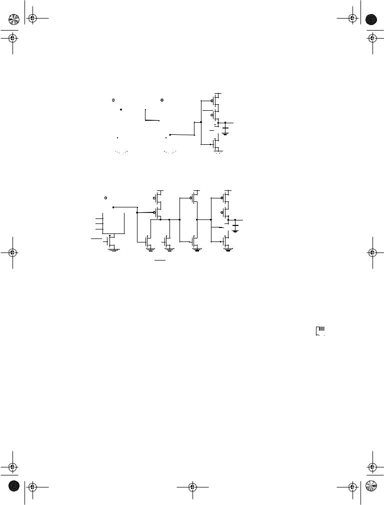
present in heavily loaded wires. There are many techniques to construct these amplifiers, with the use of feedback (e.g., cross-coupled inverters) being one common approach. The circuit shown in Figure 7.38 uses a precharged front-end amplifier that samples the differential input signal on the rising edge of the clock signal. The outputs of front-end are fed into a NAND cross-coupled SR FF that holds the data and gurantees that the differential outputs switch only once per clock cycle. The differential inputs in this implementation don’t have to have rail-to-rail swing and hence this register can be used as a receiver for a reduced swing differential bus.
The core of the front-end consists of a cross-coupled inverter (M5-M8) whose outputs (L1 and L2) are precharged using devices M9 and M10 during the low phase of the clock. As a result, PMOS transistors M7 and M8 to be turned off and the NAND FF is holding its previous state. Transistor M1 is similar to an evaluate switch in dynamic circuits and is turned off ensuring that the differential inputs don’t affect the output during the low phase of the clock. On the rising edge of the clock, the evaluate transistor turns on and the differential input pair (M2 and M3) is enabled, and the difference between the input signals is amplified on the output nodes on L1 and L2. The cross-coupled inverter pair flips to one of its the stable states based on the value of the inputs. For example, if IN is 1, L1 is pulled to 0, and L2 remains at VDD. Due to the amplifying properties of the input stage, it is not necessary for the input to swing all the way up to VDD and enables the use of lowswing signaling on the input wires.
|
|
|
|
|
|
|
|
|
|
|
|
|
|
|
|
|
|
|
|
|
0 |
|
L1 |
|
|
|
|
|
|
|
Initially |
|
|
|
|
|
|
|
|
|
|
|
|
|
|
|
|
|
|
|
||||||||||||
|
|
|
|
|
|
|
|
|
|
|
|
|
|
|
|
|
|
|
|
|
|
|
|
|
|
|
|
|
|
|
L2 |
|
1 |
|
|
|
|
|
|
|
|
|
|
|
|
|
||||||||||||||||
|
|
|
|
|
|
|
|
|
|
|
|
|
|
|
|
|
|
|
|
|
|
|
|
|
|
|
|
|
|
|
|
|
|
|
|
|
|
|
|
|
|
|
|
|
|
|
|
|
|
|
|
|
|
|
|
|||||||
|
|
|
|
|
|
|
|
|
|
|
|
|
|
|
|
|
|
|
|
|
|
|
|
|
|
|
|
|
|
|
|
|
|
|
|
|
|
|
|
|
|
|
|
|
|
|
|
|
|
|
|
|
|
|
||||||||
|
|
|
|
|
|
|
|
|
|
|
|
|
|
|
|
|
|
|
|
|
|
|
|
|
|
|
|
|
|
|
|
|
|
|
|
|
|
|
|
|
|
|
|
|
|
|
|
|
|
|
|
|
|
|
|
|
|
|||||
|
|
|
|
|
|
|
|
|
|
|
|
|
|
|
|
|
|
|
|
|
|
|
|
|
|
|
|
|
|
|
|
|
|
|
|
|
|
|
|
|
|
|
|
|
|
|
|
|
|
|
|
|
|
|
|
|
|
|
|
|||
|
|
|
|
|
|
|
|
|
|
|
|
|
|
|
|
|
high |
|
|
|
|
|
|
|
|
|
|
|
|
|
|
|
|
|
|
|
|
|
|
|
|
|
|
|
|
|
|
|
|
|
|
|
|
|
|
|
|
|
||||
|
|
|
|
|
|
|
|
|
|
|
|
|
|
|
|
|
|
|
|
|
|
|
|
|
|
|
|
|
|
|
|
|
|
|
|
|
|
|
|
|
|
|
|
|
|
|
|
|
|
|
|
|
|
|
|
|
|
|
||||
|
|
|
|
|
|
|
|
|
|
|
|
|
|
|
impedance |
|
|
|
|
|
|
|
|
|
|
|
|
|
|
|
|
|
|
|
|
|
|
|
|
|
|
|
|
|
|
|
|
|
|
|
|
|
||||||||||
|
|
|
|
|
|
|
|
|
|
|
|
|
|
|
|
0 |
|
|
|
|
|
|
|
|
|
|
1 |
|
|
0 |
|
|
|
|
|
|
|
|
|
|
|
|
|
|
|
|
|
|
||||||||||||||
|
|
|
|
|
|
|
|
|
|
|
|
|
|
|
|
|
|
IN |
|
L3 |
|
|
|
|
|
|
|
|
|
|
|
|
L4 |
|
|
|
|
|
|
|
|
|
|
|
|
|
|
|
||||||||||||||
|
|
|
|
|
|
|
|
|
|
|
|
|
|
|
|
|
|
|
|
|
|
|
|
|
|
|
|
|
|
|
|
|
|
|
|
|
|
|
|
|
|
|
|
|
|
|
|
|
|
|
|
|
|
|
|
|
||||||
|
w/o shorting |
|
|
|
|
|
|
|
|
|
|
|
|
|
|
|
|
|
|
|
|
|
|
|
|
|
|
|
|
|
|
|
IN |
|||||||||||||||||||||||||||||
|
1 |
|
0 |
|
|
|
|
|
|
|
|
|
|
|
|
|
|
|
|
|
|
|
|
|
|
|
|
|
0 |
|
|
1 |
|
|
|
|
|
|
||||||||||||||||||||||||
|
|
|
|
|
device |
|
|
|
|
|
|
|
|
|
|
|
|
|
|
|
|
|
|
|
|
|
|
|
|
|
|
|
|
|
|
|
|
|
|
|||||||||||||||||||||||
|
|
|
|
|
|
|
|
|
|
|
|
|
|
|
|
|
|
|
|
|
|
|
|
|
|
|
|
|
|
|
|
|
|
|
|
|
|
|
|
|
|
|
|
|
|
|
|
|
|
|
|
|
||||||||||
|
|
|
|
|
|
|
|
|
|
|
|
|
|
|
|
|
|
|
|
|
|
|
Inputs Change (CLK still high) |
|
|
|
|
|
|
|
|
|
|
|||||||||||||||||||||||||||||
|
|
|
|
|
|
|
|
|
|
|
|
|
|
|
|
|
|
|
|
|
|
|
|
|
|
|
|
|
|
|
|
|
|
|
|
|
|
|
|
|
|
|
|
|
|
|
|
|
|
|
|
|
|
|
|
|
|
|
|
L1 |
||
|
|
|
|
|
|
|
|
|
|
|
|
|
|
|
|
|
|
|
|
|
|
|
|
|
|
|
|
|
|
|
|
|
|
|
|
|
|
|
|
|
|
|
|
|
|
|
|
|
|
|
|
|
|
|
|
|
|
|
|
|||
|
|
|
|
|
|
|
|
|
|
|
|
|
|
|
|
|
|
|
|
|
|
|
|
|
|
|
|
|
|
|
|
|
|
|
|
|
|
|
|
|
|
|
|
|
|
|
|
|
|
|
|
|
|
|
|
|
|
|
|
|||
|
0 |
|
1 |
L1 |
|
|
|
|
|
|
|
|
|
|
|
|
|
|
|
|
L2 |
1 |
|
0 |
|
|
|
|
|
|
|
|
|
|
|
|
|
|
|
|
|
|
|
|
|
|
|
|
0 |
|
0 |
|
|
|||||||||
|
|
|
|
|
|
|
|
|
|
|
|
|
|
|
|
|
|
|
|
|
|
|
|
|
|
|
|
|
|
|
|
|
|
|
|
|
|
|
|
|
|
|
|
|
|
|
|
|
|
|
|
|
|
|
||||||||
leakage path |
|
|
|
|
|
|
|
|
|
|
|
|
|
|
|
|
|
|
|
|
|
|
|
|
|
|
|
|
|
|
|
|
|
|
|
|
leakage path |
|||||||||||||||||||||||||
|
|
|
|
|
|
|
|
|
|
|
|
|
|
|
|
|
|
|
|
|
|
|
|
|
|
|
|
|
|
|
|
|
|
|
|
|
|
|||||||||||||||||||||||||
|
|
|
|
|
|
|
|
|
|
|
|
|
|
|
|
|
|
|
|
|
|
|
|
|
|
|
|
|
|
|
|
|
|
|
|
|
|
|
|
|||||||||||||||||||||||
|
|
|
|
|
|
|
|
|
|
|
|
|
|
|
|
|
|
|
|
|
|
|
|
|
|
|
|
|
|
|
|
|
|
|
|
|
|
|
|
|
|
|
|
|
|
|
|
|
|
|
|
|
|
|
|
|
|
|
|
|
L3 |
|
|
|
|
|
|
|
L3 |
|
0 |
|
|
1 |
|
|
|
|
|
|
0 |
L4 |
|
|
|
|
|
|
|
|
|
|
|
|
|
|
|
|
|
|
|
|
|
|
|
|
|
|
|
|
IN |
|
|||||||||||||
|
|
|
|
|
|
|
|
|
|
|
|
|
|
|
|
|
|
|
|
|
|
|
|
|
|
|
|
|
|
|
|
|
|
|
|
|
|
|
|
|
|
|
|
|
||||||||||||||||||
|
|
|
|
|
|
|
|
|
|
|
|
|
|
|
|
|
|
|
|
|
|
|
|
|
|
|
|
|
|
|
|
|
|
|
|
|
|
|
|
|
|
|
|
|
|
|
|
|
|
|
|
|
|
|
|
|||||||
IN |
|
|
|
|
|
|
|
|
|
|
|
|
|
|
|
|
|
|
|
|
|
|
|
|
IN |
|
|
|
|
|
|
|
|
|
|
|
|
|
|
|
|
|
|
|
|
1 |
|
0 |
|
|
|
|
||||||||||
1 |
|
0 |
|
|
|
|
|
|
|
|
|
|
|
|
|
|
|
|
|
|
|
|
|
|
0 |
|
|
1 |
|
|
|
|
|
|
|
|
|
|
|
|
|
|
|
|
|
|
|
|
|
|
|
|
|
|
|
|
|
|
||||
|
|
|
|
|
|
|
|
|
|
|
|
|
|
|
|
|
|
|
|
|
|
|
|
|
|
|
|
|
|
|
|
|
|
|
|
|
|
|
|
|
|
|
|
|
|
|
|
|
|
|
|
|
|
|
||||||||
w/shorting device
L2 1 1
1
|
|
|
|
|
|
|
|
|
|
|
|
|
|
0 |
|
0 |
|
|
|
|
1 |
|
0 |
L4 |
|||
|
|
|
|
|
|
||||||||
|
|
|
|
|
|
|
|
|
|
|
|
|
|
IN
0 1
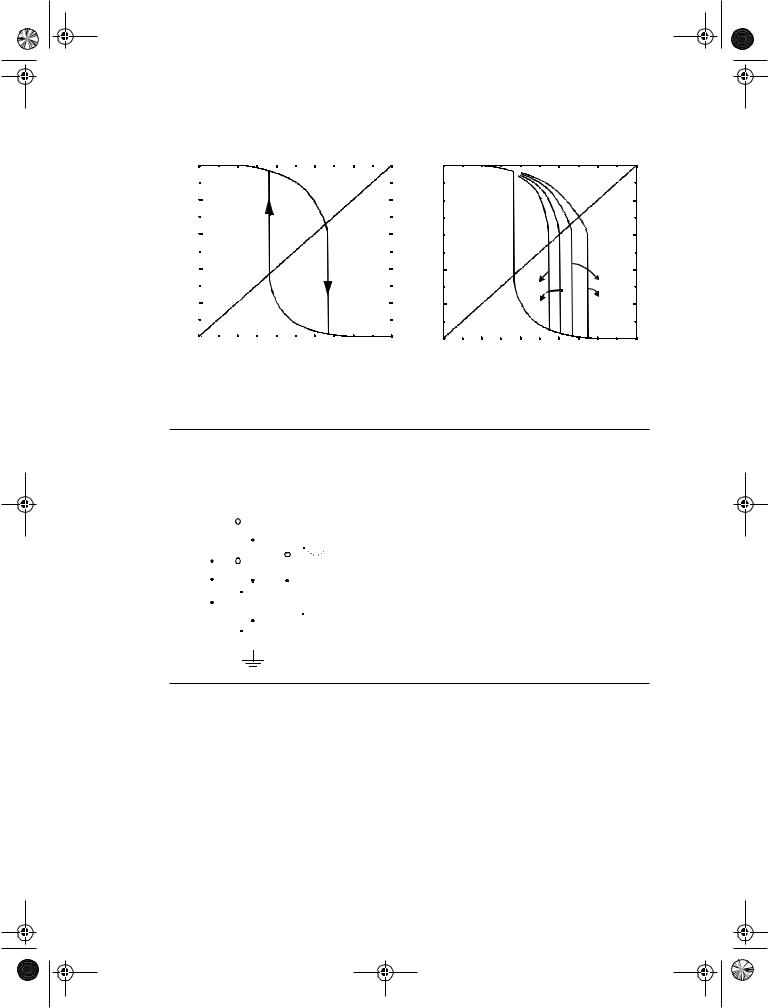
1
L3 is isolated so charge accumulates until L1/L3 change state, causing L2 to change state as well.
As a result the flip-flop outputs change.
The leakage current attempts to charge L1/L3 but the DC path through the shorting transistor allows it to leak away to ground.
Figure 7.39 The need for the shorting transistor M4.
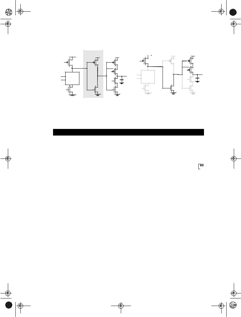
The shorting transistor, M4, is used to provide a DC leakage path from either node L3, or L4, to ground. This is necessary to accommodate the case where the inputs change their value after the positive edge of CLK has occurred, resulting in either L3 or L4 being left in a high-impedance state with a logical low voltage level stored on the node. Without the leakage path that node would be susceptible to charging by leakage currents. The latch
chapter7_pub.fm Page 301 Wednesday, November 22, 2000 8:41 AM
Section 7.8 |
Pipelining: An approach to optimize sequential circuits |
301 |
could then actually change state prior to the next rising edge of CLK! This is best illustrated graphically, as shown in Figure 7.39.
7.8Pipelining: An approach to optimize sequential circuits
Pipelining is a popular design technique often used to accelerate the operation of the datapaths in digital processors. The idea is easily explained with the example of Figure 7.40a. The goal of the presented circuit is to compute log(|a − b|), where both a and b represent streams of numbers, that is, the computation must be performed on a large set of input values. The minimal clock period Tmin necessary to ensure correct evaluation is given as:
Tmi n = tc-q + tpd,logic + ts u |
(7.6) |
where tc-q and tsu are the propagation delay and the set-up time of the register, respectively.
We assume that the registers are edge-triggered D registers. The term tpd,logic stands for the worst-case delay path through the combinatorial network, which consists of the adder,
absolute value, and logarithm functions. In conventional systems (that don’t push the edge of technology), the latter delay is generally much larger than the delays associated with the registers and dominates the circuit performance. Assume that each logic module has an equal propagation delay. We note that each logic module is then active for only 1/3 of the clock period (if the delay of the register is ignored). For example, the adder unit is active during the first third of the period and remains idle—this is, it does no useful computation— during the other 2/3 of the period. Pipelining is a technique to improve the resource utilization, and increase the functional throughput. Assume that we introduce registers between the logic blocks, as shown in Figure 7.40b. This causes the computation for one set of input data to spread over a number of clock periods, as shown in Table 7.1. The
a
b
|
REG |
|
|
|
|
|
|
|
|
|
|
|
|
|
|
|
|
|
|
|
|
|
|
|
|
|
|
|
|
CLK |
|
|
|
|
|
||||
|
|
|
. |
|
|
||||
|
|
||||||||
|
|
|
|
|
|
|
|
|
|
|
|
|
|
|
|
|
|
|
|
|
REG |
|
|
|
|
|
|
|
|
|
|
|
|
|
|
|
|
|
|
|
|
|
|
|
|
|
|
|
|
CLK |
|
|
|
|
|||||
log
|
REG |
|
|
Out |
|
|
|
|
(a) Nonpipelined version |
CLK |
|
|||
|
|
|||
a |
|
|
REG |
|
|
|
|
|
|
|
|
|
|
|
|
|
|
|
|
|
|
|
|
|
|
|
|
|
|
|
|
|
|
|
|
|
|
|
|
|
|
|
|
|
|
|
|
|
|
|
|
|
|
|
|
|
|
|
|
|
|
|
|
|
|
|
|
|
|
|
|
|
|
|
|
|
|
|
|
|
|
|
|
|
|
|
|
|
|
|
|
|
|
|
|
|
|
|
|
|
|
|
|
|
|
|
|
REG |
|
|
|
. |
|
|
|
REG |
|
|
log |
|
|
REG |
|
|
|
|
CLK |
|
|
|
|
|
|
|
|
|
|
|
|
|
Out |
||||||||
|
|
|
|
|
|
|
|
|
|
|
|
|
|
|
||||||||||
|
|
|
|
|
|
|
|
|
|
|
|
|
|
|
|
|
|
|||||||
|
|
|
|
|
|
|
|
|
|
|
|
|
|
|
|
|
|
|
|
|
|
|
|
|
|
|
|
|
|
|
|
|
|
|
|
|
|
|
|
|
|
|
|
|
|
|
|
|
|
b |
|
|
REG |
|
|
|
CLK |
|
|
|
|
CLK |
|
|
CLK |
|
||||||||
|
|
|
|
|
|
|
|
|
|
|
|
|||||||||||||
|
|
|
|
|
|
|
|
|
|
|
|
|
|
|
|
|
|
|
|
|
|
|
|
|
|
|
|
|
|
|
|
|
|
|
|
|
|
|
|
|
|
|
|
|
|
|
|
|
|
|
|
CLK |
|
|
|
|
|
|
|
|
|
|
|
|
|
|
|
|
|
|
|
|||
|
|
|
Figure 7.40 Datapath for the computation of log(|a + b|). |
|
||||||||||||||||||||
(b) Pipelined version
chapter7_pub.fm Page 302 Wednesday, November 22, 2000 8:41 AM
302 |
DESIGNING SEQUENTIAL LOGIC CIRCUITS |
Chapter 7 |
result for the data set (a1, b1) only appears at the output after three clock-periods. At that time, the circuit has already performed parts of the computations for the next data sets, (a2, b2) and (a3,b3). The computation is performed in an assembly-line fashion, hence the name pipeline.
Table 7.1 Example of pipelined computations.
Clock Period |
Adder |
Absolute Value |
Logarithm |
|
|
|
|
|
|
|
|
1 |
a1 + b1 |
|
|
2 |
a2 + b2 |
|a1 + b1| |
|
3 |
a3 + b3 |
|a2 + b2| |
log(|a1 + b1|) |
4 |
a4 + b4 |
|a3 + b3| |
log(|a2 + b2|) |
|
|
|
|
5 |
a5 + b5 |
|a4 + b4| |
log(|a3 + b3|) |
|
|
|
|
The advantage of pipelined operation becomes apparent when examining the minimum clock period of the modified circuit. The combinational circuit block has been partitioned into three sections, each of which has a smaller propagation delay than the original function. This effectively reduces the value of the minimum allowable clock period:
Tmin,pipe = tc-q + max(tpd,add,tpd,abs, tpd,log) |
(7.7) |
Suppose that all logic blocks have approximately the same propagation delay, and that the register overhead is small with respect to the logic delays. The pipelined network
outperforms the original circuit by a factor of three under these assumptions, or T min,pipe= Tmin/3. The increased performance comes at the relatively small cost of two additional reg-
isters, and an increased latency.1 This explains why pipelining is popular in the implementation of very high-performance datapaths.
7.8.1Latchvs. Register-Based Pipelines
Pipelined circuits can be constructed using level-sensitive latches instead of edge-trig- gered registers. Consider the pipelined circuit of Figure 7.41. The pipeline system is implemented based on pass-transistor-based positive and negative latches instead of edgetriggered registers. That is, logic is introduced between the master and slave latches of a master-slave system. In the following discussion, we use without loss of generality the CLK-CLK notation to denote a two-phase clock system. Latch-based systems give significantly more flexibility in implementing a pipelined system, and often offers higher performance. When the clocks CLK and CLK are nonoverlapping, correct pipeline operation is obtained. Input data is sampled on C1 at the negative edge of CLK and the computation of logic block F starts; the result of the logic block F is stored on C2 on the falling edge of
CLK, and the computation of logic block G starts. The nonoverlapping of the clocks
1 Latency is defined here as the number of clock cycles it takes for the data to propagate from the input to the output. For the example at hand, pipelining increases the latency from 1 to 3. An increased latency is in general acceptable, but can cause a global performance degradation if not treated with care.
chapter7_pub.fm Page 303 Wednesday, November 22, 2000 8:41 AM
Section 7.8 |
Pipelining: An approach to optimize sequential circuits |
303 |
|
|
CLK |
|
|
CLK |
|
CLK |
||||||||||||||||||||||||
In |
|
|
|
|
|
|
|
|
F |
|
|
|
|
|
|
|
|
|
|
|
G |
|
|
|
|
|
|
|
|
Out |
|
|
|
|
|
|
|
|
|
|
|
|
|
|
|
|
|
|
|
|
|
|
|
|
|
|
|
|
|
|
|||
|
|
|
|
|
|
|
C1 |
|
|
|
|
|
|
|
|
C2 |
|||||||||||||||
|
|
|
|
|
|
|
|
|
|
|
|
|
|
|
|
|
|
|
C |
||||||||||||
|
|
|
|
|
|
|
|
|
|
|
|
|
|
|
|
|
|
|
|
|
|
|
|
||||||||
|
|
|
|
|
|
|
|
|
|
|
|
|
|
|
|
|
|
|
|
|
|
|
|
||||||||
|
|
|
|
|
|
|
|
|
|
|
|
|
|
|
|
|
|
|
|
|
|
|
|
|
|
|
|
3 |
|
|
|
|
|
|
|
|
|
|
|
|
|
|
|
|
|
|
|
|
|
|
|
|
|
|
|
|
|
|
|
|
|
|
|
|
|
|
|
|
|
|
|
|
|
|
|
|
|
|
|
|
|
|
|
|
|
|
|
|
|
|
|
|
|
|
|
CLK
CLK
|
|
Figure 7.41 Operation of two-phase |
|
|
|
Compute F |
compute G |
pipelined circuit using dynamic registers. |
|
ensures correct operation. The value stored on C2 at the end of the CLK low phase is the result of passing the previous input (stored on the falling edge of CLK on C1) through the
logic function F. When overlap exists between CLK and CLK, the next input is already being applied to F, and its effect might propagate to C2 before CLK goes low (assuming that the contamination delay of F is small). In other words, a race develops between the previous input and the current one. Which value wins depends upon the logic function F, the overlap time, and the value of the inputs since the propagation delay is often a function of the applied inputs. The latter factor makes the detection and elimination of race conditions non-trivial.
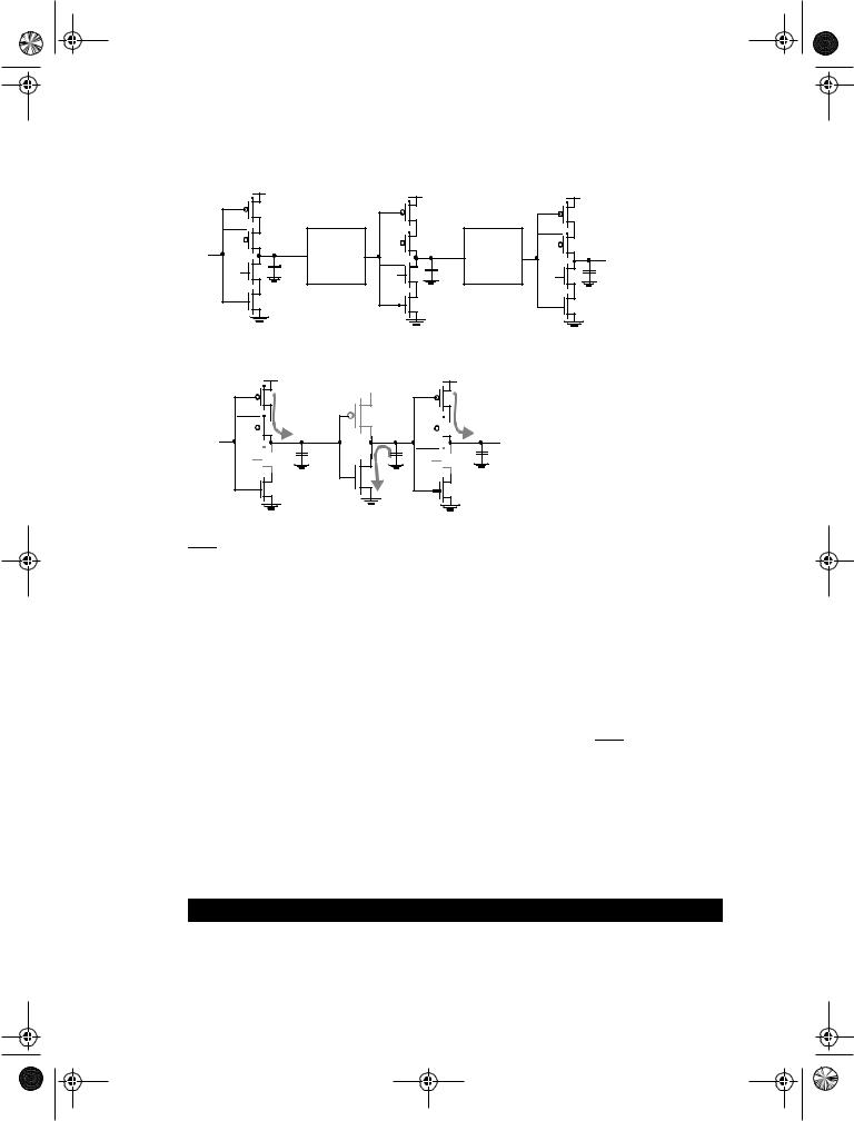
7.8.2NORA-CMOS—A Logic Style for Pipelined Structures
The latch-based pipeline circuit can also be implemented using C2MOS latches, as shown in Figure 7.42. The operation is similar to the one discussed above. This topology has one additional, important property:
A C2MOS-based pipelined circuit is race-free as long as all the logic functions F (implemented using static logic) between the latches are noninverting.
The reasoning for the above argument is similar to the argument made in the construction of a C2MOS register. During a (0-0) overlap between CLK and CLK, all C2MOS latches, simplify to pure pull-up networks (see Figure 7.27). The only way a signal can race from stage to stage under this condition is when the logic function F is inverting, as illustrated in Figure 7.43, where F is replaced by a single, static CMOS inverter. Similar considerations are valid for the (1-1) overlap.
Based on this concept, a logic circuit style called NORA-CMOS was conceived [Goncalves83]. It combines C2MOS pipeline registers and NORA dynamic logic function blocks. Each module consists of a block of combinational logic that can be a mixture of static and dynamic logic, followed by a C2MOS latch. Logic and latch are clocked in such a way that both are simultaneously in either evaluation, or hold (precharge) mode. A block
chapter7_pub.fm Page 304 Wednesday, November 22, 2000 8:41 AM
304 |
DESIGNING SEQUENTIAL LOGIC CIRCUITS |
Chapter 7 |
|
VDD |
V |
V |
|
|
DD |
DD |
|
CLK |
|
CLK |
|
CLK |
|
|
In |
F |
|
G |
|
Out |
|
CLK |
|
|
||||
C1 |
CLK |
C2 |
CLK |
C3 |
||
|
Figure 7.42 Pipelined datapath using C2MOS latches.
VDD |
VDD |
VDD |
||
|
|
|
|
|
CLK

0
CLK 

CLK

CLK

Figure 7.43 Potential race condition
during (0-0) overlap in C2MOS-based design.
that is in evaluation during CLK = 1 is called a CLK-module, while the inverse is called a CLK-module. Examples of both classes are shown in Figure 7.44 a and b, respectively. The operation modes of the modules are summarized in Table 7.2.
Table 7.2 Operation modes for NORA logic modules.
|
|
CLK block |
|
CLK block |
||
|
|
|
|
|
|
|
|
Logic |
|
Latch |
Logic |
|
Latch |
|
|
|
|
|
|
|
|
|
|
|
|
|
|
CLK = 0 |
Precharge |
|
Hold |
Evaluate |
|
Evaluate |
|
|
|
|
|
|
|
CLK = 1 |
Evaluate |
|
Evaluate |
Precharge |
|
Hold |
|
|
|
|
|
|
|
A NORA datapath consists of a chain of alternating CLK and CLK modules. While one class of modules is precharging with its output latch in hold mode, preserving the previous output value, the other class is evaluating. Data is passed in a pipelined fashion from module to module.
NORA offers designers a wide range of design choices. Dynamic and static logic can be mixed freely, and both CLKp and CLKn dynamic blocks can be used in cascaded or in pipelined form. With this freedom of design, extra inverter stages, as required in DOMINO-CMOS, are most often avoided.
Design Rules
In order to ensure correct operation, two important rules should always be followed:
chapter7_pub.fm Page 305 Wednesday, November 22, 2000 8:41 AM
Section 7.8 |
Pipelining: An approach to optimize sequential circuits |
305 |
|
|
|
|
VDD |
|
|
|
|
|
|
|
VDD |
|||||
|
CLK |
|
|
|
|
|
|
|
|
|
|
|
|
|
|
||
|
|
|
|
|
|
|
|
|
|
|
|
|
|
|
|||
In1 |
|
|
|
|
|
CLK |
|
|
|
|
|
|
|||||
|
|
|
|
|
|
|
|||||||||||
|
|
|
|
|
|
|
|
|
|
|
|
|
|
|
|
|
|
|
|
|
|
|
|
|
|
|
|
|
|
|
|
|
|
|
|
|
|
|
|
|
|
|
|
|
|
|
|
|
PUN |
|
|||
|
|
|
|
|
|
|
|
|
|
|
|
|
|
||||
|
|
|
|
|
|
|
|
|
|||||||||
In2 |
|
|
|
PDN |
|
|
|
|
|
|
|
|
|
|
|
||
|
|
|
|
|
|
|
|
|
|
|
|
|
|||||
In3 |
|
|
|
|
|
|
|
|
|
|
|
|
|
|
|
|
|
|
|
|
|
|
|
|
|
|
|
|
|
|
|
|
|
|
|
|
|
|
|
|
|
|
|
|
|
|
|
|
|
|
|
|
|
|
|
|
|
|
|
|
|
|
|
|
CLK |
|
|
|
|
|
|
|
CLK |
|
|
|
|
||||||||||||
|
|
|
|
|
|
|
|
|
|
|
|
|
|
|
|
|
|
|
|
|
|
|
|
|
|
|
|
|
|
|
|
|
|
|
|
|
|
|
|
|
|
|
|
|
|
|
|
|
|
|
|
|
|
VDD
CLK
Out
CLK 

|
|
|
|
|
|
|
|
Combinational logic |
|
Latch |
|||||
|
(a) CLK-module |
|
|
|
|
|
|
VDD |
V |
V |
|
|
|
|
V |
|
DD |
DD |
|
|
|
|
DD |
|
|
|
|
|
|
|
|
|
|
|
|
|
|
|
|
|
|
|
|
|
|
|
|
CLK |
|
|
|
|
|
|
|
|
In4 |
|
|
|
|
|
|
|
|
|
|||||
|
|
|
|
|
|
|
|
|
|
|
|
|
|
|
|
|
|
|
|
|
|
|
|
In1
In2 PDN
In3
CLK |
In4 |
|
CLK
Out
CLK 

(b) CLK-module
Figure 7.44 Examples of NORA CMOS Modules.
• The dynamic-logic rule: Inputs to a dynamic CLKn (CLKp) block are only allowed to make a single 0 → 1 (1 → 0) transition during the evaluation period (Chapter 6).
•The C2MOS rule: In order to avoid races, the number of static inversions between C2MOS latches should be even.
The presence of dynamic logic circuits requires the introduction of some extensions to the latter rule. Consider the situation pictured in Figure 7.45a. During precharge (CLK = 0), the output register of the module has to be in hold mode, isolating the output node from the internal events in the module. Assume now that a (0-0) overlap occurs. Node A gets precharged to VDD, while the latch simplifies to a pull-up network (Figure 7.45b). It can be observed that under those circumstances the output node charges to VDD, and the stored value is erased! This malfunctioning is caused by the fact that the number of static inversions between the last dynamic node in the module and the latch is odd, which creates an active path between the precharged node and the output. This translates into the following rule: The number of static inversions between the last dynamic block in a logic function and the C2MOS latch should be even. This and similar considerations lead to a reformulated C2MOS rule [Goncalvez83].
chapter7_pub.fm Page 306 Wednesday, November 22, 2000 8:41 AM
306 |
|
DESIGNING SEQUENTIAL LOGIC CIRCUITS |
Chapter 7 |
|||
VDD |
|
|
VDD |
V |
V |
|
V |
||||||
V |
DD |
DD |
||||
|
DD |
DD |
|
|
|
|
|
|
|
|
|||
|
CLK |
|
CLK |
|
|
|
A |
||
|
A |
|
||
|
|
|
||
|
CLK |
|
CLK |
|
|
In1 |
Out |
||
In1 |
Out |
|||
PDN |
||||
PDN |
In2 |
|||
In2 |
||||
CLK |
|
CLK |
||
|
|
|
||
|
CLK |
|
CLK |
|
|
|
|
(a)Circuit with odd number of static inversions between dynamic logic stage and register
Figure 7.45 Extended C2MOS rules.
(b) Same circuit during (0-0) clock overlap.
Revised C2MOS Rule
•The number of static inversions between C2MOS latches should be even (in the absence of dynamic nodes); if dynamic nodes are present, the number of static inverters between a latch and a dynamic gate in the logic block should be even. The number of static inversions between the last dynamic gate in a logic block and the latch should be even as well.
Adhering to the above rules is not always trivial and requires a careful analysis of the logic equations to be implemented. This often makes the design of an operational NORA-CMOS structure cumbersome. Its use should only be considered when maximum circuit performance is a must.
7.9Non-Bistable Sequential Circuits
In the preceding sections, we have focused on one single type of sequential element, this is the latch (and its sibling the register). The most important property of such a circuit is that it has two stable states, and is hence called bistable. The bistable element is not the only sequential circuit of interest. Other regenerative circuits can be catalogued as astable and monostable. The former act as oscillators and can, for instance, be used for on-chip clock generation. The latter serve as pulse generators, also called one-shot circuits. Another interesting regenerative circuit is the Schmitt trigger. This component has the useful property of showing hysteresis in its dc characteristics—its switching threshold is variable and depends upon the direction of the transition (low-to-high or high-to-low). This peculiar feature can come in handy in noisy environments.
chapter7_pub.fm Page 307 Wednesday, November 22, 2000 8:41 AM
Section 7.9 |
Non-Bistable Sequential Circuits |
307 |
7.9.1The Schmitt Trigger
Definition
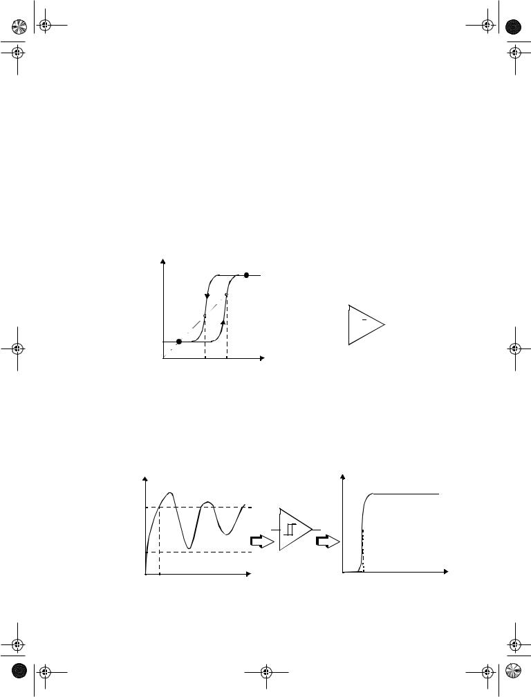
A Schmitt trigger [Schmitt38] is a device with two important properties:
1.It responds to a slowly changing input waveform with a fast transition time at the output.
2.The voltage-transfer characteristic of the device displays different switching thresholds for positiveand negative-going input signals. This is demonstrated in Figure 7.46, where a typical voltage-transfer characteristic of the Schmitt trigger is shown (and its schematics symbol). The switching thresholds for the low-to-high and high-
to-low transitions are called VM+ and VM− , respectively. The hysteresis voltage is defined as the difference between the two.
Vout |
|
VOH |
VOL |
|
|
VM– |
VM+ |
V |
|
|
in |
(a) Voltage-transfer characteristic
Figure 7.46 Non-inverting Schmitt trigger.
In |
|
|
|
|
|
|
|
Out |
|
|
|
|
|
|
(b) Schematic symbol
One of the main uses of the Schmitt trigger is to turn a noisy or slowly varying input signal into a clean digital output signal. This is illustrated in Figure 7.47. Notice how the hysteresis suppresses the ringing on the signal. At the same time, the fast low-to-high (and high-to-low) transitions of the output signal should be observed. For instance, steep signal slopes are beneficial in reducing power consumption by suppressing direct-path currents. The “secret” behind the Schmitt trigger concept is the use of positive feedback.
Vin
VM+
VM–
t0
Vout
t |
t0 + tp |
t |
Figure 7.47 Noise suppression using a Schmitt trigger.
chapter7_pub.fm Page 308 Wednesday, November 22, 2000 8:41 AM
308 |
DESIGNING SEQUENTIAL LOGIC CIRCUITS |
Chapter 7 |
CMOS Implementation
One possible CMOS implementation of the Schmitt trigger is shown in Figure 7.48. The idea behind this circuit is that the switching threshold of a CMOS inverter is determined by the (kn/kp) ratio between the NMOS and PMOS transistors. Increasing the ratio results in a reduction of the threshold, while decreasing it results in an increase in VM. Adapting the ratio depending upon the direction of the transition results in a shift in the switching threshold and a hysteresis effect. This adaptation is achieved with the aid of feedback.
|
|
|
|
|
|
|
|
VDD |
|
|
|
|
|
|
|
||||
|
|
|
|
|
|
|
|
|
|
|
|
|
|
|
|
|
|
|
|
|
|
|
|
|
|
|
|
|
|
|
|
|
|
|
|
|
|
|
|
|
|
|
|
|
|
|
|
|
|
|
|
|
|
|
|
|
|
|
|
|
|
|
|
|
|
|
M2 |
|
M4 |
|
|||||||||
|
|
|
|
||||||||||||||||
Vin |
|
|
|
|
|
|
X |
|
|
|
|
|
|
V |
|||||
|
|
|
|
|
|
|
|
|
|
|
|||||||||
|
|
|
|
|
|
|
|
|
|
|
|
|
|
|
|
|
|
|
out |
|
|
|
|
|
|
|
|
|
|
|
|
|
|
|
|
|
|
|
|
|
|
|
|
|
|
|
|
|
|
|
|
|
|
|
|
|
|
|
|
|
|
|
|
|
|
|
M1 |
|
|
|
|
M3 |
|
||||||
|
|
|
|
|
|
|
|
|
|
|
|
|
|
|
|
|
|
|
|
|
|
|
|
|
|
|
|
|
|
|
|
|
|
|
|
|
|
|
|
|
|
|
|
|
|
|
|
|
|
|
|
|
|
|
|
|
|
|
|
Figure 7.48 CMOS Schmitt trigger.
Suppose that Vin is initially equal to 0, so that Vout = 0 as well. The feedback loop biases the PMOS transistor M4 in the conductive mode while M3 is off. The input signal effectively connects to an inverter consisting of two PMOS transistors in parallel (M2 and M4) as a pull-up network, and a single NMOS transistor (M1) in the pull-down chain. This modifies the effective transistor ratio of the inverter to kM1/(kM2+kM4), which moves the switching threshold upwards.
Once the inverter switches, the feedback loop turns off M4, and the NMOS device M3 is activated. This extra pull-down device speeds up the transition and produces a clean output signal with steep slopes.
A similar behavior can be observed for the high-to-low transition. In this case, the pull-down network originally consists of M1 and M3 in parallel, while the pull-up network is formed by M2. This reduces the value of the switching threshold to VM–.
Example 7.7 CMOS Schmitt Trigger
Consider the schmitt trigger with the following device sizes. Devices M1 and M2 are 1 m/0.25 m, and 3 m/0.25 m, respectively. The inverter is sized such that the switching threshold is around VDD/2 (= 1.25 V). Figure 7.49a shows the simulation of the Schmitt trigger assuming that devices M3 and M4 are 0.5 m/0.25 m and 1.5 m/0.25 m, respectively. As apparent from the plot, the circuit exhibits hysteresis. The high-to-low switching point (VM- = 0.9 V) is lower than VDD/2, while the low-to-high switching threshold (VM+ = 1.6 V) is larger than VDD/2.
It is possible to shift the switching point by changing the sizes of M3 and M4. For example, to modify the low-to-high transition, we need to vary the PMOS device. The high- to-low threshold is kept constant by keeping the device width of M3 at 0.5 m. The device width of M4 is varied as k * 0.5 m. Figure 7.49b demonstrates how the switching threshold increases with raising values of k.
chapter7_pub.fm Page 309 Wednesday, November 22, 2000 8:41 AM
Section 7.9 |
Non-Bistable Sequential Circuits |
309 |
V (V) X
2.5 |
|
|
|
|
|
|
|
|
|
|
|
|
|
|
|
|
|
2.0 |
|
|
|
|
|
|
|
|
1.5 |
|
|
|
|
|
VM+ |
|
|
|
|
|
|
|
|
|
||
|
|
|
|
|
|
|
||
|
|
|
|
|
|
|
|
|
1.0 |
|
|
VM- |
|
|
|
|
|
|
|
|
|
|
|
|||
0.5 |
|
|
|
|
|
|
|
|
0.0 |
|
|
|
|
|
|
|
|
|
|
|
|
|
|
|
|
|
0.0 |
0.5 |
1.0 |
1.5 |
2.0 |
2.5 |
|||
Vin(V)
V (V) x
2.5 


2.0 
1.5 
1.0 |
|
|
|
|
|
|
|
|
|
|
|
k=1 |
k=3 |
|
|
0.5 |
|
|
|
k=2 |
k=4 |
|
|
|
|
|
|
|
|
||
0.0 |
|
|
|
|
|
|
|
|
|
|
|
|
|
|
|
0.0 |
0.5 |
1.0 |
1.5 |
2.0 |
2.5 |
||
Vin(V)
(a) Voltage-transfer characteristics with hysteresis. |
(b) The effect of varying the ratio of the |
|
PMOS device M4. The width is k * 0.5 m. |
Figure 7.49 Schmitt trigger simulations.
Problem 7.8 An Alternative CMOS Schmitt Trigger
Another CMOS Schmitt trigger is shown in Figure 7.50. Discuss the operation of the gate, and derive expressions for VM− and VM+.
|
|
|
|
VDD |
|
|
|
|
|
|
|
||||
|
|
|
|
|
|
|
|
|
|
|
|
|
|
|
|
|
|
|
|
|
|
|
|
|
|
|
|
|
|
|
|
|
|
|
|
|
|
M4 |
|
M6 |
|
|
|
||||
|
|
|
|
|
|
|
|
|
|
||||||
|
|
|
|
|
|
|
|
|
|
|
|
|
|||
|
|
|
|
|
|
|
|
|
|
|
|
||||
|
|
|
|
|
|
|
|
|
|
||||||
|
|
|
|
|
|
|
|
|
|
|
|
||||
|
|
|
|
|
|
|
|
|
|
|
|
|
|
|
|
In |
|
|
|
|
|
M3 |
|
|
|
|
|
|
Out |
||
|
|
|
|
|
|
|
|
|
|
|
|||||
|
|
|
|
|
|
|
|
|
|
|
|
|
|
||
|
|
|
|
|
|
|
|
|
|
|
|
|
|||
|
|
|
|
|
|
|
|
|
|||||||
|
|
|
|
|
|
|
|
|
|
|
|
|
|
|
|
|
|
|
|
|
|
M2 |
|
|
|
|
|
|
|
||
|
|
|
|
|
|
|
|
|
|
|
|
|
|||
|
|
|
|
|
|
|
|
X |
|
|
|
|
|
|
|
|
|
|
|
|
|
|
|
|
|
M5 |
|
|
|
VDD |
|
|
|
|
|
|
|
M1 |
|
|
|
|
|
|
|
||
|
|
|
|
|
|
|
|
|
|
|
|
|
|||
|
|
|
|
|
|
|
|
|
|
|
|
|
|
|
|
|
|
|
|
|
|
|
|
|
|
|
|
|
|
|
|
Figure 7.50 Alternate CMOS Schmitt trigger.
7.9.2Monostable Sequential Circuits
A monostable element is a circuit that generates a pulse of a predetermined width every time the quiescent circuit is triggered by a pulse or transition event. It is called monostable because it has only one stable state (the quiescent one). A trigger event, which is either a signal transition or a pulse, causes the circuit to go temporarily into another quasi-stable state. This means that it eventually returns to its original state after a time period determined by the circuit parameters. This circuit, also called a one-shot, is useful in generating pulses of a known length. This functionality is required in a wide range of applications. We have already seen the use of a one-shot in the construction of glitch registers. Another