

chapter7_pub.fm Page 290 Wednesday, November 22, 2000 8:41 AM
290 |
DESIGNING SEQUENTIAL LOGIC CIRCUITS |
Chapter 7 |
One important consideration for such a dynamic register is that the storage nodes (i.e., the state) has to be refreshed at periodic intervals to prevent a loss due to charge leakage, due to diode leakage as well as sub-threshold currents. In datapath circuits, the refresh rate is not an issue since the registers are periodically clocked, and the storage nodes are constantly updated.
Clock overlap is an important concern for this register. Consider the clock waveforms shown in Figure 7.25. During the 0-0 overlap period, the NMOS of T1 and the PMOS of T2 are simultaneously on, creating a direct path for data to flow from the D input of the register to the Q output. This is known as a race condition. The output Q can change on the falling edge if the overlap period is large — obviously an undesirable effect for a positive edge-triggered register. The same is true for the 1-1 overlap region, where an input-output path exists through the PMOS of T1 and the NMOS of T2. The latter case is taken care off by enforcing a hold time constraint. That is, the data must be stable during the high-high overlap period. The former situation (0-0 overlap) can be addressed by making sure that there is enough delay between the D input and node 2 ensuring that new data sampled by the master stage does not propagate through to the slave stage. Generally the built in single inverter delay should be sufficient and the overlap period constraint is given as:
tover lap0 – 0 < tT1 + tI1 + tT 2 |
(7.4) |
Similarly, the constraint for the 1-1 overlap is given as: |
|
thold > tove rlap1 – 1 |
(7.5) |
(0,0) overlap
CLK
(1,1) overlap
CLK
Figure 7.25 Impact of non-overlapping clocks.
7.5.2C2MOS Dynamic Register: A Clock Skew Insensitive Approach
The C2MOS Register
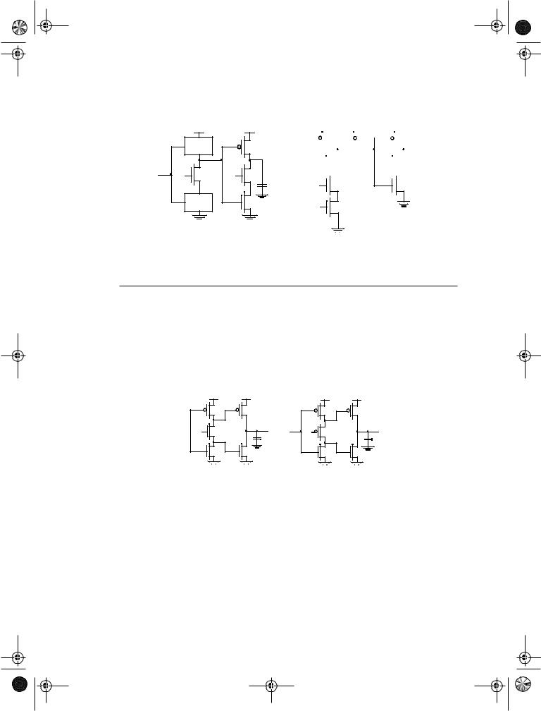
Figure 7.26 shows an ingenious positive edge-triggered register based on the master-slave concept which is insensitive to clock overlap. This circuit is called the C2MOS (Clocked CMOS) register [Suzuki73]. The register operates in two phases.
1.CLK = 0 (CLK = 1): The first tri-state driver is turned on, and the master stage acts as an inverter sampling the inverted version of D on the internal node X. The master stage is in the evaluation mode. Meanwhile, the slave section is in a high-impedance
mode, or in a hold mode. Both transistors M7 and M8 are off, decoupling the output from the input. The output Q retains its previous value stored on the output capacitor
CL2.
chapter7_pub.fm Page 291 Wednesday, November 22, 2000 8:41 AM
Section 7.5 |
Dynamic Latches and Registers |
|
|
|
|
|
|
|
291 |
||||||||||||||||||||||||||||||||||||||
|
|
|
|
|
|
|
|
|
|
|
|
VDD |
|
|
|
|
|
|
|
VDD |
|||||||||||||||||||||||||||
|
|
|
|
|
|
|
|
|
|
|
|
|
|
|
|
|
|
|
|
|
|
|
|
|
|
|
|
|
|
|
|
|
|
|
|
|
|
|
|
|
|
|
|
|
|
|
|
|
|
|
|
|
|
|
|
|
|
|
|
|
|
|
|
|
|
|
|
|
|
|
|
|
|
|
|
|
|
|
|
|
|
|
|
|
|
|
|
|
|
|
|
|
|
|
|
|
|
|
|
|
|
|
|
|
|
|
|
|
|
M2 |
|
|
|
|
|
|
|
|
M6 |
||||||||||||||||||||||||
|
|
|
CLK |
|
|
|
|
|
|
|
|
|
|
|
|
|
|||||||||||||||||||||||||||||||
|
|
|
|
|
|
|
|
|
|
|
|
|
|
|
|
|
|
|
|
|
|
|
|
|
|
|
|
|
|
|
|
|
|
|
|
|
|
|
|
|
|
|
|
||||
|
|
|
|
|
|
|
|
|
|
|
|
|
|
|
|
|
|
|
|
|
|
|
|
|
|
|
|
|
|
|
|
|
|
|
|
|
|
|
|
|
|
|
|
||||
|
|
|
|
|
|
|
|
|
|
|
|
|
|
|
|
|
|
|
|
|
|
|
|
|
|
|
|
|
|
|
|
|
|
|
|
|
|
|
|
|
|
|
|||||
|
|
|
|
|
|
|
|
|
M4 |
CLK |
|
|
|
|
|
M8 |
|||||||||||||||||||||||||||||||
|
|
|
|
|
|
||||||||||||||||||||||||||||||||||||||||||
|
D |
|
|
|
|
|
|
|
|
|
|
|
|
|
|
|
|
|
|
|
|
X |
|
|
|
|
|
|
|
|
|
|
|
|
|
|
|
|
|
|
|
|
|
Q |
|||
|
|
|
|
|
|
|
|
|
|
|
|
|
|
|
|
|
|
|
|
|
|
|
|
|
|
|
|
|
|
|
|
|
|
|
|
||||||||||||
|
|
|
|
|
|
|
|
|
|
|
|
|
|
|
|
|
|
|
|
|
|
|
|
|
|
|
|
|
|
|
|
|
|
|
|
|
|
|
|
|
|
|
|
||||
|
|
|
|
|
|
|
|
|
|
|
|
|
|
|
|
|
|
|
|
|
|
|
|
|
|
|
|
|
|
|
|
|
|
|
|
|
|||||||||||
|
|
|
|
|
|
|
|
|
|
|
|
|
|
|
|
|
|
|
|
|
|
|
|
|
CL1 |
|
|
|
|
|
|
|
|
|
|
|
|
|
|
|
|
|
|
|
|
CL2 |
|
|
|
|
CLK |
|
|
|
|
|
|
M3 |
|
|
|
CLK |
|
|
|
|
M7 |
|
|
|
|
||||||||||||||||||||||||
|
|
|
|
|
|
|
|
|
|
|
|
|
|
|
|
|
|
||||||||||||||||||||||||||||||
|
|
|
|
|
|
|
|
|
|
|
|
|
|
|
|
|
|
|
|
|
|
|
|
|
|
|
|
|
|
|
|
|
|
|
|
|
|
|
|
|
|
|
|
|
|
|
|
|
|
|
|
|
|
|
|
|
|
|
|
|
|
|
|
|
|
|
|
|
|
|
|
|
|
|
|
|
|
|
|
|
|
|
|
|
|
|
|
|
|
|
|
|
|
|
|
|
|
|
|
|
|
|
|
|
|
|
|
|
|
|
|
|
|
|
|
|
|
|
|
|
|
|
|
|
|
|
|
|
|
|
|
|
|
|
|
|
|
|
|
|
|
|
|
|
|
|
|
|
|
|
|
|
|
|
|
|
|
M1 |
|
|
|
|
|
|
|
|
M5 |
||||||||||||||||||||||||
|
|
|
|
|
|
|
|
|
|
|
|
|
|
|
|
|
|
|
|
||||||||||||||||||||||||||||
|
|
|
|
|
|
|
|
|
|
|
|
|
|
|
|
|
|
|
|
|
|
|
|
|
|
|
|
|
|
|
|
|
|
|
|
|
|
|
|
|
|
|
|
|
|
|
|
|
|
|
|
|
|
|
|
|
|
|
|
|
|
|
|
|
|
|
|
|
|
|
|
|
|
|
|
|
|
|
|
|
|
|
|
|
|
|
|
|
|
|
|
|
|
|
|
|
|
|
|
|
|
|
|
|
|
|
|
|
|
|
|
|
|
|
|
|
|
|
|
|
|
|
|
|
|
|
|
|
|
|
|
|
|
|
|
|
|||||||
|
|
|
|
|
|
|
|
|
|
|
|
|
|
|
|
|
|
|
|
|
|
|
|
|
|
|
|
|
|
|
|
|
|
|
|
|
|
|
|
|
|
|
|
|
|
|
|
|
|
|
|
|
|
|
|
|
|
|
|
|
|
|
|
||||||||||||||||||||||||||||||||
|
|
|
|
|
Master Stage |
|
Slave Stage |
||||||||||||||||||||||||||||||||||||||||
|
Figure 7.26 C2MOS master-slave positive edge-triggered register. |
||||||||||||||||||||||||||||||||||||||||||||||
2.The roles are reversed when CLK = 1: The master stage section is in hold mode (M3- M4 off), while the second section evaluates (M7-M8 on). The value stored on CL1 propagates to the output node through the slave stage which acts as an inverter.
The overall circuit operates as a positive edge-triggered master-slave register — very similar to the transmission-gate based register presented earlier. However, there is an important difference:
A C2MOS register with CLK-CLK clocking is insensitive to overlap, as long as the rise and fall times of the clock edges are sufficiently small.
To prove the above statement, we examine both the (0-0) and (1-1) overlap cases (Figure 7.25). In the (0-0) overlap case, the circuit simplifies to the network shown in Figure 7.27a in which both PMOS devices are on during this period. The question is does any new data sampled during the overlap window propagate to the output Q. This is not desirable since data should not change on the negative edge for a positive edge-triggered register. Indeed new data is sampled on node X through the series PMOS devices M2-M4, and node X can make a 0-to-1 transition during the overlap period. However, this data cannot propagate to the output since the NMOS device M7 is turned off. At the end of the overlap
period, CLK=1 and both M7 and M8 turn off, putting the slave stage is in the hold mode. Therefore, any new data sampled on the falling clock edge is not seen at the slave output Q, since the slave state is off till the next rising edge of the clock. As the circuit consists of a cascade of inverters, signal propagation requires one pull-up followed by a pull-down, or vice-versa, which is not feasible in the situation presented.
The (1-1) overlap case (Figure 7.27b), where both NMOS devices M3 and M7 are turned on, is somewhat more contentious. The question is again if new data sampled during the overlap period (right after clock goes high) propagates to the Q output. A positive edge-triggered register may only pass data that is presented at the input before the rising
chapter7_pub.fm Page 292 Wednesday, November 22, 2000 8:41 AM
292 |
DESIGNING SEQUENTIAL LOGIC CIRCUITS |
Chapter 7 |
edge. If the D input changes during the overlap period, node X can make a 1-to-0 transition, but cannot propagate to the output. However, as soon as the overlap period is over, the PMOS M8 is turned on and the 0 propagates to output. This effect is not desirable. The
|
VDD |
|
VDD |
VDD |
|
VDD |
|
|
M |
|
|
M |
M2 |
|
M |
|
2 |
|
|
|
6 |
||
|
|
|
6 |
|
|
|
|
0 |
M4 |
0 |
M8 |
X |
|
|
|
D |
|
|
X |
Q D |
|
Q |
|
|
|
|
|
|
|||
|
|
|
|
1 |
M3 |
1 |
M |
|
|
|
|
|
7 |
||
|
M |
1 |
|
M |
M1 |
|
M |
|
|
|
5 |
|
|
5 |
|
|
|
(a) (0-0) overlap |
|
(b) (1-1) overlap |
|
|
|
Figure 7.27 C2MOS D FF during overlap periods. No feasible signal path can exist between In and D, as illustrated by the arrows.
problem is fixed by imposing a hold time constraint on the input data, D, or, in other words, the data D should be stable during the overlap period.
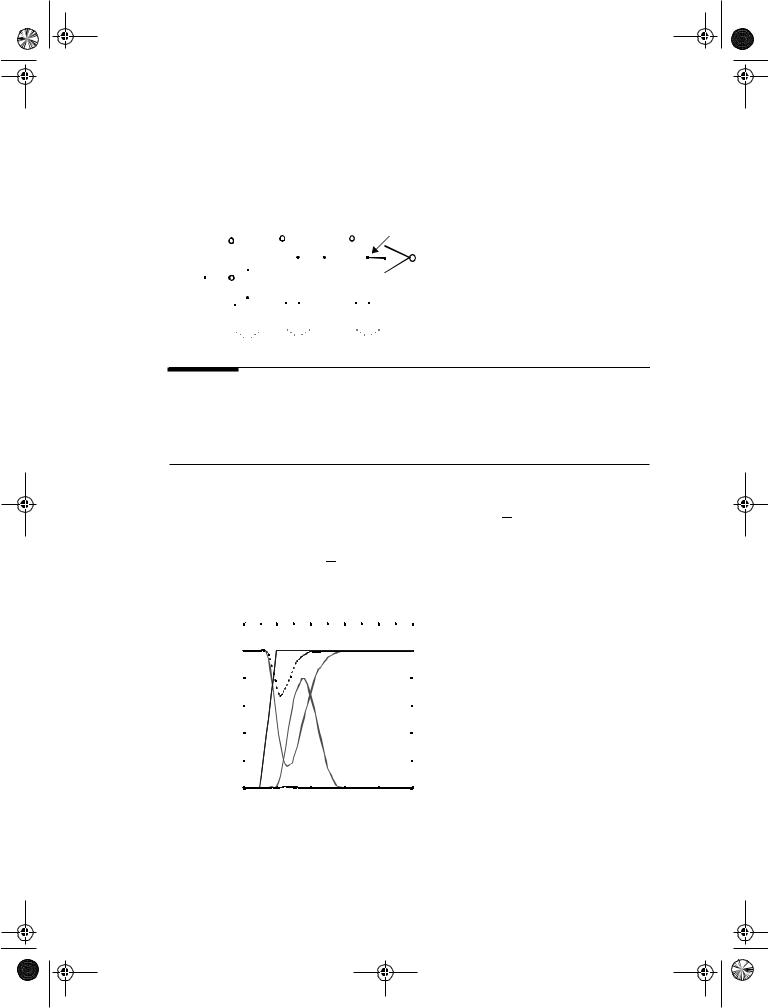
In summary, it can be stated that the C2MOS latch is insensitive to clock overlaps because those overlaps activate either the pull-up or the pull-down networks of the latches, but never both of them simultaneously. If the rise and fall times of the clock are sufficiently slow, however, there exists a time slot where both the NMOS and PMOS transistors are conducting. This creates a path between input and output that can destroy the state of the circuit. Simulations have shown that the circuit operates correctly as long as the clock rise time (or fall time) is smaller than approximately five times the propagation delay of the register. This criterion is not too stringent, and is easily met in practical designs. The impact of the rise and fall times is illustrated in Figure 7.28, which plots the simulated transient response of a C2MOS D FF for clock slopes of respectively 0.1 and 3 nsec. For slow clocks, the potential for a race condition exists.
|
3.0 |
|
|
|
|
|
2.5 |
|
|
Q(3) |
|
|
|
X(3) |
|
|
|
|
2.0 |
|
|
|
|
|
|
|
|
|
|
|
1.5 |
|
CLK(3) |
|
|
Volts |
|
|
|
Q(0.1) |
|
|
X(0.1) |
|
CLK(0.1) |
||
|
|
|
|||
|
1.0 |
|
|
|
|
|
|
|
|
|
|
|
0.5 |
|
|
|
|
|
0.0 |
|
|
|
|
|
-0.5 |
|
|
|
|
|
0 |
2 |
4 |
6 |
8 |
|
|
|
time (nsec) |
|
|
Figure 7.28 Transient response of C2MOS FF for 0.1 nsec and 3 nsec clock rise (fall) times assuming In = 1.
chapter7_pub.fm Page 293 Wednesday, November 22, 2000 8:41 AM
Section 7.5 |
Dynamic Latches and Registers |
293 |
Dual-edge Triggered Registers
So far, we have focused on edge-triggered registers that sample the input data on only one of the clock edges (rising or falling). It is also possible to design sequential circuits that sample the input on both edges. The advantage of this scheme is that a lower frequency clock (half of the original rate) is distributed for the same functional throughput, resulting in power savings in the clock distribution network. Figure 7.29 shows a modification of the C2MOS register to enable sampling on both edges [REFERENCE]. It consists of two parallel master-slave based edge-triggered registers, whose outputs are multiplexed using the tri-state drivers.
When clock is high, the positive latch composed of transistors M1-M4 is sampling the inverted D input on node X. Node Y is held stable, since devices M9 and M10 are turned off. On the falling edge of the clock, the top slave latch M5-M8 turns on, and drives the inverted value of X to the Q output. During the low phase, the bottom master latch (M1, M4, M9, M10) is turned on, sampling the inverted D input on node Y. Note that the devices M1 and M4 are reused, reducing the load on the D input. On the rising edge, the bottom slave latch conducts, and drives the inverted version of Y on node Q. Data hence changes on both edges. Note that the slave latches operate in a complementary fashion — this is, only one of them is turned on during each phase of the clock.
VDD |
VDD |
|
M4 |
|
|
M |
|
|
|
|
8 |
|
n1 |
|
|
|
CLK |
M3 X |
|
CLK |
M7 |
D |
|
|
|
|
CLK |
M2 |
|
CLK |
M |
|
n2 |
|
|
6 |
|
|
|
|
|
|
M1 |
|
|
M |
|
|
|
|
5 |
|
|
|
VDD |
|
|
n1 |
|
|
M14 |
CLK |
M10 |
Y |
CLK |
M13 |
CLK |
M9 |
|
CLK |
M12 |
|
|
|||
|
n2 |
|
|
M11 |
|
|
|
|
Q
Figure 7.29 C2MOS based dual-edge triggered register.
Problem 7.6 Dual-edge Registers
Determine how the adoption of dual-edge registers influences the power-dissipation in the clock-distribution network.
chapter7_pub.fm Page 294 Wednesday, November 22, 2000 8:41 AM
294 |
DESIGNING SEQUENTIAL LOGIC CIRCUITS |
Chapter 7 |
7.5.3True Single-Phase Clocked Register (TSPCR)
In the two-phase clocking schemes described above, care must be taken in routing the two clock signals to ensure that overlap is minimized. While the C2MOS provides a skew-tol- erant solution, it is possible to design registers that only use a single phase clock. The True Single-Phase Clocked Register (TSPCR) proposed by Yuan and Svensson uses a single clock (without an inverse clock) [Yuan89]. The basic single-phase positive and negative latches are shown in Figure 7.30. For the positive latch, when CLK is high, the latch is in
V |
V |
VDD |
VDD |
DD |
|
DD |
|
|
|
Out |
|
In |
CLK |
In |
CLK |
|
|||
CLK |
|
|
CLK
Out
Negative Latch
Positive Latch
Figure 7.30 True Single Phase Latches.
the transparent mode and corresponds to two cascaded inverters; the latch is non-invert- ing, and propagates the input to the output. On the other hand, when CLK = 0, both inverters are disabled, and the latch is in hold-mode. Only the pull-up networks are still active, while the pull-down circuits are deactivated. As a result of the dual-stage approach, no signal can ever propagate from the input of the latch to the output in this mode. A register can be constructed by cascading positive and negative latches. The clock load is similar to a conventional transmission gate register, or C2MOS register. The main advantage is the use of a single clock phase. The disadvantage is the slight increase in the number of transistors — 12 transistors are required.
TSPC offers an additional advantage: the possibility of embedding logic functionality into the latches. This reduces the delay overhead associated with the latches. Figure 7.31a outlines the basic approach for embedding logic, while Figure 7.31b shows an example of a positive latch that implements the AND of In1 and In2 in addition to performing the latching function. While the set-up time of this latch has increased over the one shown in Figure 7.30, the overall performance of the digital circuit (that is, the clock period of a sequential circuit) has improved: the increase in set-up time is typically smaller than the delay of an AND gate. This approach of embedding logic into latches has been used extensively in the design of the EV4 DEC Alpha microprocessor [Dobberpuhl92] and many other high performance processors.
Example 7.4 Impact of embedding logic into latches on performance
Consider embedding an AND gate into the TSPC latch, as shown in Figure 7.31b. In a 0.25m, the set-up time of such a circuit using minimum-size devices is 140 psec. A conventional approach, composed of an AND gate followed by a positive latch has an effective set-up time of 600 psec (we treat the AND plus latch as a black box that performs the AND+latching
chapter7_pub.fm Page 295 Wednesday, November 22, 2000 8:41 AM
Section 7.5 |
Dynamic Latches and Registers |
295 |
VDD |
VDD |
|
|
PUN |
|
|
Q |
In |
CLK |
CLK |
|
||
|
|
PDN |
|
|
|
|
|
|
|
VDD |
|
|
|
|
|
|
|
|
|
|
VDD |
|||||
In1 |
|
|
|
|
|
|
|
|
|
|
|
In2 |
|
|
|
|
|||||||
|
|
|
|
|
|
|
|
|
|
|
|
||||||||||||
|
|
|
|
|
|
|
|
|
|
||||||||||||||
|
|
|
|
|
|
|
|
|
|
|
|
|
|
|
|
CLK |
|
|
|
|
Q |
||
CLK |
|
|
|
|
|
|
|
|
|
|
|
|
|
|
|
|
|
||||||
|
|
|
|
|
|
||||||||||||||||||
|
|
|
|
|
|
|
|
|
|
|
|
|
|
|
|
|
|
|
|
|
|
|
|
|
|
|
|
|
|
|
|
|
|
|
|
|
|
|
|
|
|
|
|
|
|
|
|
|
|
|
|
|
|
|
|
|
|
|
|
|
|
|
|
|
|
|
|
|
|
|
|
In1
In2
(a) Including logic into the latch |
|
(b) AND latch |
Figure 7.31 Adding logic to the TSPC approach.
functions). The embedded logic approach hence results in significant performance improvements.
The TSPC latch circuits can be further reduced in complexity as illustrated in Figure 7.32, where only the first inverter is controlled by the clock. Besides the reduced number of transistors, these circuits have the advantage that the clock load is reduced by half. On the other hand, not all node voltages in the latch experience the full logic swing. For instance, the voltage at node A (for Vin = 0 V) for the positive latch maximally equals VDD
– VTn, which results in a reduced drive for the output NMOS transistor and a loss in performance. Similarly, the voltage on node A (for Vin = VDD) for the negative latch is only driven down to |VTp|. This also limits the amount of VDD scaling possible on the latch.
VDD |
VDD |
V |
DD |
V |
|
|
|
DD |
In
 CLK
CLK
A
Out |
In |
CLK |
A |
Out |
|
|
|
|
|
|
|
|
|
|
|
|
|
|
|
|
|
|
|
|
|
|
(a) Positive Latch |
(b) Negative Latch |
||||||||||||||||
Figure 7.32 Simplified TSPC latch (also called split-output).
Figure 7.33 shows the design of a specialized single-phase edge-triggered register. When CLK = 0, the input inverter is sampling the inverted D input on node X. The second (dynamic) inverter is in the precharge mode, with M6 charging up node Y to VDD. The third inverter is in the hold mode, since M8 and M9 are off. Therefore, during the low phase of the clock, the input to the final (static) inverter is holding its previous value and the output Q is stable. On the rising edge of the clock, the dynamic inverter M4-M6 evaluates. If X is high on the rising edge, node Y discharges. The third inverter M7-M8 is on during the high phase, and the node value on Y is passed to the output Q. On the positive phase of the clock, note that node X transitions to a low if the D input transitions to a high level. Therefore, the input must be kept stable till the value on node X before the rising edge of the clock propagates to Y. This represents the hold time of the register (note that the hold time less than 1 inverter delay since it takes 1 delay for the input to affect node X). The propa-
chapter7_pub.fm Page 296 Wednesday, November 22, 2000 8:41 AM
296 |
DESIGNING SEQUENTIAL LOGIC CIRCUITS |
Chapter 7 |
gation delay of the register is essentially three inverters since the value on node X must propagate to the output Q. Finally, the set-up time is the time for node X to be valid, which is one inverter delay.
|
|
|
|
|
VDD |
|
|
|
|
|
|
VDD |
|
|
|
|
|
VDD |
|||||||||||||||
|
|
|
|
|
|
|
|
|
|
|
|
|
|
|
|
|
|
|
|
|
|
|
|
|
|
|
|
|
|
|
|||
|
|
|
|
|
|
|
|
CLK |
|
|
|
|
|
|
|
|
|
|
|
|
|
|
|
|
Q |
|
|||||||
|
|
|
|
|
M |
|
|
|
|
|
|
|
M6 |
|
|
|
|
|
|
M |
|||||||||||||
D |
|
|
|
|
3 |
|
|
|
|
|
|
|
|
|
|
Y |
|
|
|
|
|
9 |
|
|
|
|
|
Q |
|||||
CLK |
|
|
|
|
X |
|
|
|
|
|
CLK |
|
|
|
|
|
|
|
|
|
|
|
|
||||||||||
|
|
|
M5 |
|
|
|
|
|
|
|
|
|
|
|
|
||||||||||||||||||
M |
|
|
|
|
|
|
M |
||||||||||||||||||||||||||
|
|
|
|
|
|
|
|
|
|
|
|
|
|
|
|
|
|
||||||||||||||||
|
|
|
|
|
2 |
|
|
|
|
|
|
|
|
|
|
|
|
|
|
|
8 |
|
|
|
|
|
|
||||||
|
|
|
|
|
|
|
|
|
|
|
|
|
|
|
|
|
|
|
|
|
|
|
|
|
|
|
|
|
|
|
|
|
|
|
|
|
|
|
|
|
|
|
|
|
|
|
|
|
|
|
|
|
|
|
|
|
|
|
|
|
|
|
|
|
|
|
|
|
|
|
|
|
M |
|
CLK |
|
M4 |
|
|
|
|
|
|
|
M |
||||||||||||||||
|
|
|
|
|
|
|
|
|
|
|
|
|
|
|
|
|
|
|
|||||||||||||||
|
|
|
|
|
|
|
|
|
|
|
|
|
|
|
|
|
|
||||||||||||||||
|
|
|
|
|
|
|
|
|
|
|
|
|
|
|
|
|
|
|
|
7 |
|
|
|
|
|
|
|||||||
|
|
|
|
|
1 |
|
|
|
|
|
|
|
|
|
|
|
|
|
|
|
|
|
|
|
|
|
|
Figure 7.33 Positive edge-triggered register |
|||||
|
|
|
|
|
|
|
|
|
|
|
|
|
|
|
|
|
|
|
|
|
|
|
|
|
|
|
|
|
|
||||
|
|
|
|
|
|
|
|
|
|
|
|
|
|
|
|
|
|
|
|
|
|
|
|
|
|
|
|
|
|
TSPC. |
|||
WARNING: Similar to the C2MOS latch, the TSPC latch malfunctions when the slope of the clock is not sufficiently steep. Slow clocks cause both the NMOS and PMOS clocked transistors to be on simultaneously, resulting in undefined values of the states and race conditions. The clock slopes should therefore be carefully controlled. If necessary, local buffers must be introduced to ensure the quality of the clock signals.
Example 7.5 TSPC Edge-Triggered Register
Transistor sizing is critical for achieving correct functionality in the TSPC register. With improper sizing, glitches may occur at the output due to a race condition when the clock transitions from low to high. Consider the case where D is low and Q=1 (Q=0). While CLK is low, Y is pre-charged high turning on M7. When CLK transitions from low to high, nodes Y and Q start to discharge simultaneously (through M4-M5 and M7-M8, respectively). Once Y is suffi-
ciently low, the trend on Q is reversed and the node is pulled high anew through M9. In a sense, this chain of events is comparable to what would happen if we chain dynamic logic gates. Figure 7.34 shows the transient response of the circuit of Figure 7.34 for different sizes of devices in the final two stages.
Volts
3.0 |
|
|
|
|
|
|
|
modified |
|
|
|
|
|
|
|
|
|
|
|
|
|
|
|
|
|
|
|
|
|
|
|
|
|||
|
|
|
|
|
|
|
|
|
|
|
|
|
|
|
|
||
|
|
|
|
|
|
Q |
|
|
|
|
|
|
|||||
|
|
|
|
|
|
Q |
original |
|
|
|
|
|
|
||||
2.0 |
|
|
|
|
|
|
|
|
|
|
|
|
|
|
|
M4, M5 |
M7, M8 |
|
|
|
|
|
|
|
|
|
|
|
|
|
|
|
|
||
|
|
|
|
|
|
|
|
|
|
|
|
|
|
|
|||
|
|
|
|
|
|
|
|
|
|
|
|
|
|
|
|||
|
|
CLK |
|
|
|
|
|
|
|
|
|
Original |
0.5 m |
2 m |
|||
1.0 |
|
|
|
|
|
|
|
|
|
|
|
|
|
|
Width |
|
|
|
|
|
|
|
|
|
|
|
|
|
|
|
|
|
|
|
|
|
|
|
|
|
|
|
|
|
|
Qoriginal |
|
|
|
Modified |
1 m |
1 m |
|
|
|
|
|
|
|
|
|
|
|
|
|
|
|
|
Width |
|
|
|
|
|
|
|
|
|
|
|
Qmodified |
|
|
|
|
|
|
||
|
|
|
|
|
|
|
|
|
|
|
|
|
|
|
|||
0.0 |
|
0.2 |
0.4 |
0.6 |
0.8 |
1.0 |
|
|
|
||||||||
0.0 |
|
|
|
||||||||||||||
time (nsec)
Figure 7.34 Transistor sizing issues in TSPC (for the register of Figure 7.33).
This glitch may be the cause of fatal errors, as it may create unwanted events (for instance, when the output of the latch is used as a clock signal input to another register). It also reduces the contamination delay of the register. The problem can be corrected by resizing the relative strengths of the pull-down paths through M4-M5 and M7-M8, so that Y discharges
chapter7_pub.fm Page 297 Wednesday, November 22, 2000 8:41 AM
Section 7.6 |
Pulse Registers |
297 |
much faster than Q. This is accomplished by reducing the strength of the M7-M8 pulldown path, and by speeding up the M4 -M5 pulldown path.
7.6Pulse Registers
Until now, we have used the master-slave configuration to create an edge-triggered register. A fundamentally different approach for constructing a register uses pulse signals. The idea is to construct a short pulse around the rising (or falling) edge of the clock. This pulse acts as the clock input to a latch (e.g., a TSPC flavor is shown in Figure 7.35a), sampling the input only in a short window. Race conditions are thus avoided by keeping the opening time (i.e, the transparent period) of the latch very short. The combination of the glitchgeneration circuitry and the latch results in a positive edge-triggered register.
Figure 7.35b shows an example circuit for constructing a short intentional glitch on each rising edge of the clock [Kozo96]. When CLK = 0, node X is charged up to VDD (MN is off since CLKG is low). On the rising edge of the clock, there is a short period of time when both inputs of the AND gate are high, causing CLKG to go high. This in turn activates MN, pulling X and eventually CLKG low (Figure 7.35c). The length of the pulse is controlled by the delay of the AND gate and the two inverters. Note that there exists also a delay between the rising edges of the input clock (CLK) and the glitch clock (CLKG) — also equal to the delay of the AND gate and the two inverters. If every register on the chip uses the same clock generation mechanism, this sampling delay does not matter. However, process variations and load variations may cause the delays through the glitch clock circuitry to be different. This must be taken into account when performing timing verification and clock skew analysis (which is the topic of a later Chapter).
|
|
|
|
|
|
|
|
|
|
|
VDD |
|
VDD |
|
|
|
|
|
|
|
|
|
|
|
|
|
|
|
|
|
|
|
|
|
|
|
|||||||||||||
|
|
|
|
|
|
|
|
|
|
|
|
|
|
|
|
|
|
|
|
|
|
|
|
|
|
|
|
|
|
|
|
|
|
VDD |
|
|
|
|
|
||||||||||
|
|
|
|
|
|
|
|
|
M3 |
|
|
|
|
M6 |
|
CLK |
|
|
|
|
|
|
|
|
|
|
|
||||||||||||||||||||||
|
|
|
|
|
|
|
|
|
|
|
|
|
|
||||||||||||||||||||||||||||||||||||
|
|
|
|
|
|
|
|
|
|
|
|
|
|
|
|
|
|
|
|
|
|
|
|
|
|
|
|
Q |
|
|
|
|
|
|
|
|
|
|
|
|
|
|
|
|
CLKG |
||||
D |
|
|
CLKG |
|
|
|
|
|
|
|
|
|
|
CLKG |
|
|
|
|
|
|
|
|
|
|
|
|
|
|
MP X |
|
|
|
|
|
|
|
|
|
|||||||||||
|
|
|
|
|
|
M2 |
|
|
|
|
|
|
M5 |
|
|
|
|
|
|
|
|
|
|
|
|
|
|
|
|
|
|
|
|
|
|
|
|||||||||||||
|
|
|
|
|
|
|
|
|
|
|
|
|
|
|
|
|
|
|
|
|
|
|
|
|
|
|
|
|
|
|
|
|
|
|
|
|
|||||||||||||
|
|
|
|
|
|
|
|
|
|
|
|
|
|
|
|
|
|
|
|
|
|
|
|
|
|
|
|
|
|
|
|
|
|
|
|
|
|
|
|
|
|
|
|
|
|
|
|
|
|
|
|
|
|
|
|
|
|
|
|
|
|
|
|
|
|
|
|
|
|
|
|
|
|
|
|
|
|
|
|
|
|
|
MN |
|
|
|
|
|
|
|
|
|
|
|
|
|
|||
|
|
|
|
|
|
|
|
|
|
|
|
|
|
|
|
|
|
|
|
|
|
|
|
|
|
|
|
|
|
|
|
|
|
|
|
|
|
|
|
|
|
|
|
|
|
||||
|
|
|
|
|
|
|
|
|
|
|
|
|
|
|
|
|
|
|
|
|
|
|
|
|
|
|
|
|
|
|
|
|
|
|
|
|
|
|
|
|
|
|
|
|
|
|
|
|
|
|
|
|
|
|
|
|
|
|
M1 |
|
|
|
|
M4 |
|
|
|
|
|
|
|
|
|
|
|
|
|
|
|
|
|
|
|
|
|
|
|
||||||||||||
|
|
|
|
|
|
|
|
|
|
|
|
|
|
|
|
|
|
|
|
|
|
|
|
|
|
|
|
|
|
|
|
|
|
|
|
|
|
|
|
|
|
|
|
|
|
|
|
|
|
|
|
|
|
|
|
|
|
|
|
|
|
|
|
|
|
|
|
|
|
|
|
|
|
|
|
|
|
|
|
|
|
|
|
|
(b) glitch generation |
|
|
|
|
||||||||||
|
|
|
|
|
|
|
|
|
|
|
|
|
|
|
|
|
|
|
|
|
|
|
|
|
|
|
|
|
|
|
|
|
|
|
|||||||||||||||
|
|
|
|
|
|
|
|
|
|
|
|
|
|
|
|
|
|
|
|
|
|
|
|
|
|
|
|
|
|
|
|
||||||||||||||||||
|
|
|
|
|
|
|
|
|
|
|
|
|
|
|
|
|
|
|
|
|
|
|
|
|
|
|
|
|
|
|
|
|
|
|
|
|
|
|
|||||||||||
|
|
|
|
|
|
|
|
(a) register |
|
|
|
|
|
|
|
|
|
|
|
|
|
|
|
|
|
|
|||||||||||||||||||||||
|
|
CLK |
|
|
|
|
|
|
|
|
|
|
|
|
|
|
|
|
|
|
|
|
|
|
|
|
|
|
|
|
|
|
|
|
|
|
|
|
|
|
|
|
|
|
|||||
|
|
|
|
|
|
|
|
|
|
|
|
|
|
|
|
|
|
|
|
|
|
|
|
|
|
|
|
|
|
|
|
|
|
|
|
|
|
|
|
|
|
|
|
||||||
|
|
|
|
|
|
|
|
|
|
|
|
|
|
|
|
|
|
|
|
|
|
|
|
|
|
|
|
|
|
|
|
|
|
|
|
|
|
|
|
|
|
|
|
|
|
|
|
|
|
CLKG
(c) glitch clock
Figure 7.35 Glitch latch - timing generation and register.
chapter7_pub.fm Page 298 Wednesday, November 22, 2000 8:41 AM
298 |
DESIGNING SEQUENTIAL LOGIC CIRCUITS |
Chapter 7 |
If set-up time and hold time are measured in reference to the rising edge of the glitch clock, the set-up time is essentially zero, the hold time is equal to the length of the pulse (if the contamination delay is zero for the gates), and the propagation delay (tc-q) equals two gate delays. The advantage of the approach is the reduced clock load and the small number of transistors required. The glitch-generation circuitry can be amortized over multiple register bits. The disadvantage is a substantial increase in verification complexity. This has prevented a wide-spread use. They do however provide an alternate approach to conventional schemes, and have been adopted in some high performance processors (e.g., [Kozo96]).
Another version of the pulsed register is shown in Figure 7.36 (as used in the AMDK6 processor [Partovi96]). When the clock is low, M3 and M6 are off and device P1 is turned on. Node X is precharged to VDD, the output node (Q) is decoupled from X and is
held at its previous state. CLKD is a delay-inverted version of CLK. On the rising edge of the clock, M3 and M6 turn on while devices M1 and M4 stay on for a short period, determined by the delay of the three inverters. During this interval, the circuit is transparent and the input data D is sampled by the latch. Once CLKD goes low, node X is decoupled from the D input and is either held or starts to precharge to VDD by PMOS device P2. On the falling edge of the clock, node X is held at VDD and the output is held stable by the cross-coupled inverters.
|
|
|
|
|
|
|
|
|
|
|
|
|
|
|
|
|
|
|
|
|
|
|
|
|
|
|
|
|
|
|
|
|
|
|
|
CLK |
|
|
|
|
|
|
|
|
|
|
|
P1 |
x |
|
|
|
|
|
P3 |
Q |
|||||||||||||||
|
|
|
|
|
|
|
|
|
|
|
|
|
|
|
|
||||||||||||||||||||
|
|
|
|
|
|
|
|
|
|
|
|
|
|
|
|
|
|
|
|
|
|
|
|
|
|
|
|
|
|
|
|
|
|
|
|
D |
|
|
|
|
|
|
|
|
|
|
|
|
M3 |
|
|
|
|
|
|
|
|
|
|
|
M6 |
|
|
|
|
|
|
|
|||
|
|
|
|
|
|
|
|
|
|
|
|
|
|
|
|
|
|
|
|
|
|
|
|
|
|
|
|
|
|
||||||
|
|
|
|
|
|
|
|
|
|
|
|
|
|
|
|
|
|
|
|
|
|
|
|
|
|
|
|
|
|
|
|
|
|||
|
|
|
|
|
|
|
|
|
|
|
|
|
|
|
|
|
|
|
|
|
|
|
|
|
|
|
|
|
|
|
|
|
|||
|
|
|
|
|
|
|
|
|
|
|
|
|
|
|
|
|
|
|
|
|
|
|
|
|
|
|
|
|
|
|
|
||||
|
|
|
|
|
|
|
|
|
|
|
|
|
P2 |
|
|
|
M5 |
|
|
|
|
|
|
|
|||||||||||
|
|
|
|
|
|
|
|
|
|
|
|
|
M2 |
|
|
|
|
|
|
|
|
|
|
Figure 7.36 Flow-through positive |
|||||||||||
|
|
|
|
|
|
|
|
|
|
|
|
|
|
|
|
|
|
|
|
|
|
|
|
|
|
|
|
|
|
|
|
||||
|
|
|
|
|
|
|
|
|
|
|
|
|
|
|
|
|
|
|
|
|
|
|
|
|
|
|
|
|
|
|
|
|
|
||
|
|
|
|
|
|
|
|
|
|
|
|
|
|
|
|
|
|
|
|
|
|
|
|
|
|
|
M4 |
|
|
|
|
|
edge-triggered register. |
||
|
|
|
|
|
|
|
|
|
|
|
|
|
M1 |
|
|
|
|
|
|
|
|
|
|
|
|||||||||||
|
|
|
|
|
|
|
|
|
|
|
|
|
CLKD |
|
|
|
|
|
|
|
|
|
|
|
|
||||||||||
Note that this circuit also uses a one-shot, but the one-shot is integrated into the register. The transparency period also determines the hold time of the register. The window must be wide enough for the input data to propagate to the Q output. In this particular circuit, the set-up time can be negative. This is the case if the transparency window is longer than the delay from input to output. This is attractive, as data can arrive at the register even after the clock goes high, which means that time is borrowed from the previous cycle.
Example 7.6 Set-up time of glitch register
The glitch register of Figure 7.36 is transparent during the (1-1) overlap of CLK and CLKD. As a result, the input data can actually change after the rising edge of the clock, resulting in a negative set-up time (Figure 7.37). The D-input transitions to low after the rising edge of the clock, and transitions high before the falling edge of CLKD (this is, during the transparency period). Observe how the output follows the input. The output Q does go to the correct value of VDD as long as the input D is set up correctly some time before the falling edge of CLKD. When the negative set-up time is exploited, there can be no gurantees on the monotonic behavior of the output. That is, the output can have multiple transitions around the rising edge, and therefore, the output of the register should not be used as a clock to other registers.
chapter7_pub.fm Page 299 Wednesday, November 22, 2000 8:41 AM
Section 7.7 |
Sense-Amplifier Based Registers |
299 |
Volts
3.0 |
|
|
|
|
|
|
|
|
|
|
|
|
|
|
|
|
|
|
|
|
|
|
|
|
|
2.5 |
|
|
|
|
|
|
|
|
|
|
|
|
2.0 |
|
D |
|
|
|
|
|
Q |
|
|
|
|
|
|
|
|
|
|
|
|
|
||||
|
|
|
|
|
|
|
|
|
|
|
|
|
1.5 |
|
|
|
|
|
|
|
|
|
|
|
|
1.0 |
|
|
|
|
|
|
|
|
|
|
|
|
0.5 |
|
|
|
|
|
|
|
|
|
|
|
|
|
CLK |
|
CLKD |
|
|
|
|
|||||
0.0 |
|
|
|
|
|
|
|
|
|
|
|
Figure 7.37 Simulation showing a |
|
|
|
|
|
|
|
|
|
|
|
negative set-up time for the glitch |
|
|
|
|
|
|
|
|
|
|
|
|
|
|
-0.5 |
|
|
|
|
|
|
|
|
|
|
|
register. |
|
0.2 |
|
|
0.4 |
0.6 |
|
|
|
0.8 |
1.0 |
||
0.0 |
|
|
|
|
|
|||||||
time (nsec)
Problem 7.7 Converting a glitch register to a conditional glitch register
Modify the circuit in Figure 7.36 so that it takes an additional Enable input. The goal is to convert the register to a conditional register which latches only when the enable signal is asserted.
7.7Sense-Amplifier Based Registers
So far, we have presented two fundamental approaches towards building edge-triggered registers: the master-slave concept and the glitch technique. Figure 7.38 introduces another technique that uses a sense amplifier structure to implement an edge-triggered register [Montanaro96]. Sense amplifier circuits accept small input signals and amplify them to generate rail-to-rail swings. As we will see, sense amplifier circuits are used extensively in memory cores and in low swing bus drivers to amplify small voltage swings
|
OUT |
OUT |
|
|
VDD |
VDD |
|||
M9 |
M7 |
M8 |
M10 |
|
L1 |
|
|
L2 |
|
M5 |
|
|
M6 |
|
|
|
M4 |
|
|
IN |
L3 |
L4 |
IN |
|
M2 |
M3 |
|||
|
|
|||
|
|
VDD |
|
|
CLK |
|
M1 |
|
|
Figure 7.38 Positive edge-triggered register based on sense-amplifier.