

C H A P T E R
6
D E S I G N I N G C O M B I N A T I O N A L L O G I C G A T E S I N C M O S
In-depth discussion of logic families in CMOS—static and dynamic, pass-transistor, nonratioed and ratioed logic
n
Optimizing a logic gate for area, speed, energy, or robustness
n
Low-power and high-performance circuit-design techniques
6.1 |
Introduction |
|
6.3.2 Speed and Power Dissipation of |
|
6.2 |
Static CMOS Design |
|
Dynamic Logic |
|
|
6.3.3 Issues in Dynamic Design |
|||
|
6.2.1 |
Complementary CMOS |
|
|
|
|
6.3.4 Cascading Dynamic Gates |
||
|
6.5 |
Leakage in Low Voltage Systems |
|
|
|
|
|
||
|
6.2.2 |
Ratioed Logic |
6.4 |
Perspective: How to Choose a Logic Style |
|
6.2.3 |
Pass-Transistor Logic |
6.6 |
Summary |
6.3 |
Dynamic CMOS Design |
6.7 |
To Probe Further |
|
|
6.3.1 |
Dynamic Logic: Basic Principles |
6.8 |
Exercises and Design Problems |
|
|
|
||
197
198 |
DESIGNING COMBINATIONAL LOGIC GATES IN CMOS |
Chapter 6 |
6.1Introduction
The design considerations for a simple inverter circuit were presented in the previous chapter. In this chapter, the design of the inverter will be extended to address the synthesis of arbitrary digital gates such as NOR, NAND and XOR. The focus will be on combinational logic (or non-regenerative) circuits that have the property that at any point in time, the output of the circuit is related to its current input signals by some Boolean expression (assuming that the transients through the logic gates have settled). No intentional connection between outputs and inputs is present.
In another class of circuits, known as sequential or regenerative circuits —to be discussed in a later chapter—, the output is not only a function of the current input data, but also of previous values of the input signals (Figure 6.1). This is accomplished by connecting one or more outputs intentionally back to some inputs. Consequently, the circuit “remembers” past events and has a sense of history. A sequential circuit includes a combinational logic portion and a module that holds the state. Example circuits are registers, counters, oscillators, and memory.
|
|
Combinational |
In |
|
Combinational |
|
|
Out |
|||
In |
|
Logic |
Out |
|
Logic |
|
|
|
|||
|
|
Circuit |
|
|
|
|
Circuit |
|
|
|
|
|
|
|
|
|
|
|
|
|
|
|
|
|
|
|
|
|
|
|
|
|
|
|
|
|
|
|
|
|
|
|
|
|
|
|
|
|
(a) Combinational |
|
|
|
|
State |
|
|
|
|
|
|
|
|
|
|
|
|
|
|
|||
|
|
|
|
|
|
|
|
|
|
||
|
|
|
|
|
(b) Sequential |
|
|
|
|||
Figure 6.1 High level classification of logic circuits.
There are numerous circuit styles to implement a given logic function. As with the inverter, the common design metrics by which a gate is evaluated include area, speed, energy and power. Depending on the application, the emphasis will be on different metrics (e.g., in high performance processor, the switching speed of digital circuits is the primary metric while in a battery operated circuit it is the energy dissipation). In addition to these metrics, robustness to noise is also a very important consideration. We will see that certain logic styles (e.g., Dynamic logic) can significantly improve performance, but can be more sensitive to noise. Recently, power dissipation has also become a very important requirement and significant emphasis is placed on understanding the sources of power and approaches to deal with power.
6.2Static CMOS Design
The most widely used logic style is static complementary CMOS. The static CMOS style is really an extension of the static CMOS inverter to multiple inputs. In review, the primary advantage of the CMOS structure is robustness (i.e, low sensitivity to noise), good performance, and low power consumption (with no static power consumption). As we will
Section 6.2 Static CMOS Design |
199 |
see, most of those properties are carried over to large fan-in logic gates implemented using the same circuit topology.
The complementary CMOS circuit style falls under a broad class of logic circuits called static circuits in which at every point in time (except during the switching transients), each gate output is connected to either VDD or Vss via a low-resistance path. Also, the outputs of the gates assume at all times the value of the Boolean function implemented by the circuit (ignoring, once again, the transient effects during switching periods). This is in contrast to the dynamic circuit class, that relies on temporary storage of signal values on the capacitance of high-impedance circuit nodes. The latter approach has the advantage that the resulting gate is simpler and faster. On the other hand, its design and operation are more involved than those of its static counterpart, due to an increased sensitivity to noise.
In this section, we sequentially address the design of various static circuit flavors including complementary CMOS, ratioed logic (pseudo-NMOS and DCVSL), and passtransistor logic. The issues of scaling to lower power supply voltages and threshold voltages will also be dealt with.
6.2.1Complementary CMOS
A static CMOS gate is a combination of two networks, called the pull-up network (PUN) and the pull-down network (PDN) (Figure 6.2). The figure shows a generic N input logic gate where all inputs are distributed to both the pull-up and pull-down networks. The function of the PUN is to provide a connection between the output and VDD anytime the output of the logic gate is meant to be 1 (based on the inputs). Similarly, the function of the PDN is to connect the output to VSS when the output of the logic gate is meant to be 0. The PUN and PDN networks are constructed in a mutually exclusive fashion such that one and only one of the networks is conducting in steady state. In this way, once the transients have settled, a path always exists between VDD and the output F, realizing a high output (“one”), or, alternatively, between VSS and F for a low output (“zero”). This is equivalent to stating that the output node is always a low-impedance node in steady state.
In constructing the PDN and PUN networks, the following observations should be kept in mind:
|
VDD |
|
||
In1 |
|
|
|
|
|
|
|
||
In2 |
PUN |
pull-up: make a connection from VDD to F when |
||
|
F(In1,In2, ... Inn) = 1 |
|||
InN |
|
|
||
|
|
F (In1,In2, ... Inn) |
||
In1 |
|
|
||
|
|
|
||
In2 |
PDN |
pull-down: make a connection from VDD to Vss when |
||
|
||||
InN |
F(In1,In2, ... Inn) = 0 |
|||
|
|
|||
|
|
|
||
|
|
|
|
|
VSS
Figure 6.2 Complementary logic gate as a combination of a PUN (pull-up network) and a PDN (pull-down network).
200 |
DESIGNING COMBINATIONAL LOGIC GATES IN CMOS |
Chapter 6 |
•A transistor can be thought of as a switch controlled by its gate signal. An NMOS switch is on when the controlling signal is high and is off when the controlling signal is low. A PMOS transistor acts as an inverse switch that is on when the controlling signal is low and off when the controlling signal is high.
•The PDN is constructed using NMOS devices, while PMOS transistors are used in the PUN. The primary reason for this choice is that NMOS transistors produce “strong zeros,” and PMOS devices generate “strong ones”. To illustrate this, consider the examples shown in Figure 6.3. In Figure 6.3a, the output capacitance is ini-
tially charged to VDD. Two possible discharge scenario’s are shown. An NMOS device pulls the output all the way down to GND, while a PMOS lowers the output
no further than |VTp| — the PMOS turns off at that point, and stops contributing discharge current. NMOS transistors are hence the preferred devices in the PDN. Similarly, two alternative approaches to charging up a capacitor are shown in Figure 6.3b, with the output load initially at GND. A PMOS switch succeeds in charging
the output all the way to VDD, while the NMOS device fails to raise the output above VDD-VTn. This explains why PMOS transistors are preferentially used in a PUN.
|
|
|
|
|
Out |
VDD→ 0 |
|
Out VDD→ |VTp| |
|||||||||
VDD |
|
|
|
|
|
|
CL |
|
|
|
|
|
|
|
CL |
||
|
|
|
|
|
|
|
|
|
|
|
|
|
|||||
|
|
|
|
|
|
|
|
|
|
|
|
|
|||||
(a) pulling down a node using NMOS and PMOS switches |
|||||||||||||||||
VDD |
|
|
|
0→ VDD- VTn |
|
|
|
|
|
|
|
|
0 → VDD |
||||
|
|
|
|
|
|
|
|
|
|
|
|
|
|||||
|
|
|
|
|
|
|
|
|
|
|
|
|
|||||
|
|
|
|
|
|
|
|
|
|
|
|
|
|||||
|
|
|
|
|
Out |
|
CL |
|
|
|
|
Out |
|||||
|
|
|
|
|
|
|
|
|
|
CL |
|||||||
|
|
|
|
|
|
|
|
|
|
|
|
||||||
|
|
|
|
|
|
|
|
|
|
|
|
||||||
|
|
|
|
|
|
|
|
|
|
|
|
||||||
|
|
|
|
|
|
|
|
|
|
|
|
|
|
|
|
|
|
|
|
|
|
|
|
|
|
|
|
|
|
|
|
|
|
|
|
(b) pulling down a node using NMOS and PMOS switches
Figure 6.3 Simple examples illustrate why an NMOS should be used as a pulldown transistor, while a PMOS should be used as a pull-up device.
•A set of construction rules can be derived to construct logic functions (Figure 6.4). NMOS devices connected in series corresponds to an AND function. With all the inputs high, the series combination conducts and the value at one end of the chain is transfered to the other end. Similarly, NMOS transistors connected in parallel represent an OR function. A conducting path exists between the output and input terminal if at least one of the inpurs is high. Using similar arguments, construction rules for PMOS networks can be formulated. A series connection of PMOS conducts if both
Section 6.2 |
Static CMOS Design |
|
|
|
|
|
|
|
|
|
|
|
201 |
|||||
|
|
|
B |
|
A |
|
|
|
|
|
|
|||||||
|
|
|
|
|
|
|
|
|
|
|||||||||
|
|
|
|
|
|
|
|
|
|
|||||||||
|
Series Combination |
|
|
|
|
|
A |
|
|
B |
|
|
Parallel Combination |
|||||
|
|
|
|
|
|
|
|
|
|
|||||||||
|
Conducts if A · B |
|
|
|
|
|
|
|
|
|
|
|
|
|
||||
|
|
|
|
|
|
|
|
|
|
|
|
|
|
Conducts if A + B |
||||
|
|
|
|
(a) series |
|
|
|
|
|
|
||||||||
|
|
|
|
|
|
|
|
|||||||||||
|
|
|
|
|
(b) parallel |
|
||||||||||||
|
Figure 6.4 NMOS logic rules — series devices implement an AND, and parallel devices |
|||||||||||||||||
|
implement an OR. |
|
|
|
|
|
|
|
|
|
|
|
|
|||||
inputs are low, representing a NOR function (A.B = A+B), while PMOS transistors in parallel implement a NAND (A+B = A·B.
•Using De Morgan’s theorems ((A + B) = A·B and A·B = A + B), it can be shown that the pull-up and pull-down networks of a complementary CMOS structure are dual networks. This means that a parallel connection of transistors in the pull-up network corresponds to a series connection of the corresponding devices in the pull-down network, and vice versa. Therefore, to construct a CMOS gate, one of the networks (e.g., PDN) is implemented using combinations of series and parallel devices. The other network (i.e., PUN) is obtained using duality principle by walking the hierarchy, replacing series subnets with parallel subnets, and parallel subnets with series subnets. The complete CMOS gate is constructed by combining the PDN with the PUN.
•The complementary gate is naturally inverting, implementing only functions such as NAND, NOR, and XNOR. The realization of a non-inverting Boolean function (such as AND OR, or XOR) in a single stage is not possible, and requires the addition of an extra inverter stage.
•The number of transistors required to implement an N-input logic gate is 2N.
Example 6.1 Two input NAND Gate
Figure 6.5 shows a two-input NAND gate (F = A·B). The PDN network consists of two NMOS devices in series that conduct when both A and B are high. The PUN is the dual network, and consists of two parallel PMOS transistors. This means that F is 1 if A = 0 or B = 0, which is equivalent to F = A·B. The truth table for the simple two input NAND gate is given in Table 6.1. It can be verified that the output F is always connected to either VDD or GND, but never to both at the same time.
Example 6.2 Synthesis of complex CMOS Gate
Using complementary CMOS logic, consider the synthesis of a complex CMOS gate whose function is F = D + A· (B +C). The first step in the synthesis of the logic gate is to derive the pull-down network as shown in Figure 6.6a by using the fact that NMOS devices in series implements the AND function and parallel device implements the OR function. The next step is to use duality to derive the PUN in a hierarchical fashion. The PDN network is broken into smaller networks (i.e., subset of the PDN) called sub-nets that simplify the derivation of the PUN. In Figure 6.6b, the subnets (SN) for the pull-down network are identified At the top level, SN1 and SN2 are in parallel so in the dual network, they will be in series. Since SN1
202 |
|
|
|
|
|
DESIGNING COMBINATIONAL LOGIC GATES IN CMOS |
Chapter 6 |
||||||||||
|
|
|
|
|
|
VDD |
|
|
|
|
|
|
|
||||
A |
|
|
|
B |
|
|
|
Table 6.1Truth Table for 2 input NAND |
|||||||||
|
|
|
|
|
|
||||||||||||
|
|
|
|
|
|
A |
|
B |
|
F |
|
|
|||||
|
|
|
|
|
|
|
|
|
|
|
|
|
|
|
|||
|
|
|
|
|
|
|
|
|
|
|
|
||||||
|
|
|
|
|
|
|
|
|
|
|
|
||||||
|
|
|
|
|
|
|
|
|
|
F |
0 |
|
0 |
|
1 |
|
|
|
A |
|
|
|
|
|
|
0 |
|
1 |
|
1 |
|
|
|||
|
|
|
|
|
|
|
|
|
|
|
|||||||
|
|
|
|
|
|
|
|
||||||||||
|
|
|
|
|
|
|
1 |
|
0 |
|
1 |
|
|
||||
|
|
|
|
|
|
|
|
|
|
|
|
|
|
|
|||
|
|
|
|
|
|
|
|
|
|
|
|
||||||
|
|
|
|
|
|
|
|
|
|
|
1 |
|
1 |
|
0 |
|
|
|
|
|
|
|
|
|
|
|
|
|
|
|
|
|
|||
|
|
|
|
|
|
|
|
|
|
|
|
||||||
|
B |
|
|
|
|
|
|
|
|
|
|
|
|
|
|||
|
|
|
|
|
|
|
|
|
|
|
|
|
|
||||
|
|
|
|
|
|
|
|
|
|
|
|
|
|
|
|
|
|
|
|
|
|
|
|
|
|
|
|||||||||
|
|
Figure 6.5 Two-input NAND gate in complementary static CMOS style. |
|
||||||||||||||
consists of a single transistor, it maps directly to the pull-up network. On the other hand, we need to recursively apply the duality rules to SN2. Inside SN2, we have SN3 and SN4 in series so in the PUN they will appear in parallel. Finally, inside SN3, the devices are in parallel so they will appear in series in the PUN. The complete gate is shown in Figure 6.6c. The reader can verify that for every possible input cobmination, there always exists a path to either VDD or GND.
D |
|
|
|
A |
|
|
|
|
|
F |
||
|
|
|
|
|||||||||
|
|
|
|
|
|
|
|
|
||||
|
|
|
|
|
|
|
|
|
||||
|
|
|
|
|
|
|
|
|
|
|
|
|
|
|
|
B |
|
|
|
C |
|
|
|
||
|
|
|
|
|
|
|
|
|
|
|
|
|
(a) pull-down network
SN1 |
|
F |
|
|
|
|
|
|
|
|
SN4 |
|
D |
|
|
|
A |
|
|
|
|
|
SN2 |
||
|
|
|
|
|||||||||
|
|
|
|
|
||||||||
|
|
|
|
|
|
|
|
SN3 |
||||
|
|
|
|
|
|
|
|
|||||
|
|
|
|
|
|
|
|
|
|
|
||
|
B |
|
|
|
C |
|||||||
|
|
|
|
|
|
|
||||||
|
|
|
|
|
|
|
|
|
||||
|
|
|
|
|
|
|
|
|
||||
|
|
|
|
|
|
|
|
|
|
|
|
|
(b) Deriving the pull-up network hierarchically by identifying subnets
Figure 6.6 Complex complementary CMOS gate.
|
|
|
|
VDD |
|
|
|
|
|
VDD |
|||||
A |
|
|
|
|
C |
|
|
|
|||||||
|
|
|
|
|
|
|
|||||||||
|
|
|
|
||||||||||||
|
|
|
|
B |
|
|
|
|
|
||||||
|
|
|
|
|
|
|
|
|
|||||||
|
|
|
|
|
|
|
|
|
|
||||||
|
|
|
|
|
|
|
|||||||||
|
|
|
|
|
|
|
|
|
|
|
|
|
|
||
|
|
|
|
|
|
|
|
|
|
|
|
|
|
|
|
|
|
|
|
|
|
|
|
|
|
|
|
|
|
|
|
|
D |
|
|
|
|
|
|
|
|
|
|
|
|||
|
|
|
|
|
|
|
|
|
|
|
|
||||
|
|
|
|
|
|
|
|
|
|
|
|
||||
|
|
|
|
|
|
|
|
|
|
|
|
|
|
|
F |
|
|
|
|
|
|
|
|
|
|
|
|
|
|
|
|
|
|
|
|
|
|
|
|
|
|
|
|
|
|
|
|
D |
|
|
|
|
|
|
A |
|
|
|
|
|
|||
|
|
|
|
|
|
|
|
|
|
|
|
||||
|
|
|
|
|
|
|
|
|
|
|
|
||||
|
|
|
|
|
|
|
|
|
|
|
|
|
|
|
|
|
|
|
|
B |
|
|
|
C |
|
|
|||||
|
|
|
|
|
|
|
|
|
|||||||
|
|
|
|
|
|
|
|
|
|
|
|
|
|
|
|
(c) complete gate
Static Properties of Complementary CMOS Gates
Complementary CMOS gates inherit all the nice properties of the basic CMOS inverter, discussed earlier.They exhibit rail to rail swing with VOH = VDD and VOL = GND. The circuits also have no static power dissipation, since the circuits are designed such that the pull-down and pull-up networks are mutually exclusive. The analysis of the DC voltage transfer characteristics and the noise margins is more complicated then for the inverter, as these parameters depend upon the data input patterns applied to gate.
Consider the static two-input NAND gate shown in Figure 6.7. Three possible input combinations switch the output of the gate from high-to-low: (a) A = B = 0 → 1, (b) A= 1,
Section 6.2 Static CMOS Design |
203 |
|
|
|
|
|
|
VDD |
|||||
A |
|
|
|
|
B |
|
|
|
|
||
|
M3 |
|
M4 |
||||||||
|
|
|
|
|
|
|
|||||
|
|
|
|
|
|
|
|
|
|
|
|
|
|
|
|
|
|
|
|
|
|
|
|
|
|
|
|
|
|
|
|
|
|
|
|
|
|
|
|
|
|
|
|
|
|
|
F |
|
|
|
|
|
|
|
|
|
|
|
|
|
|
|
|
|
|
|
|
|
|
|
|
A |
|
M2 |
|||||||||
|
|
|
|
|
|
|
|
|
|
int |
|
|
|
|
|
|
|
||||||
|
|
|
|
|
|
|
|
|
|
||
|
|
|
|
||||||||
B |
|
M1 |
|||||||||
|
|
|
|
|
|
|
|
|
|
|
|
|
|
|
|
|
|
|
|
|
|
|
|
Vout, V
3.0 
A = B = 0→1
2.0 
A=1, B=0→1
1.0 
B=1, A=0→1
0.0 |
1.0 |
2.0 |
3.0 |
0.0 |
Vin, V
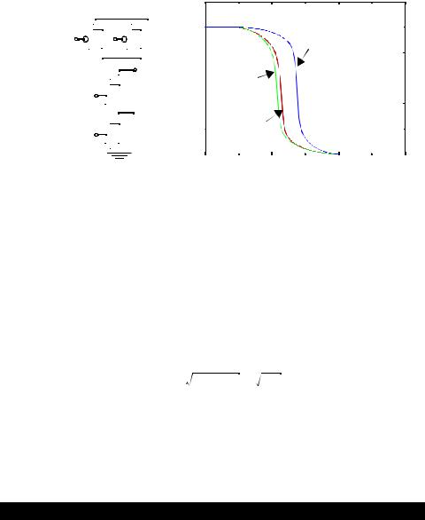
Figure 6.7 The VTC of a two-input NAND is data-dependent. NMOS devices are 0.5μm/0.25μm while the PMOS devices are sized at 0.75μm/0.25μm.
B = 0 → 1, and (c) B= 1, A = 0 → 1. The resulting voltage transfer curves display significant differences. The large variation between case (a) and the others (b & c) is explained by the fact that in the former case both transistors in the pull-up network are on simultaneously for A=B=0, representing a strong pull-up. In the latter cases, only one of the pullup devices is on. The VTC is shifted to the left as a result of the weaker PUN.
The difference between (b) and (c) results mainly from the state of the internal node int between the two NMOS devices. For the NMOS devices to turn on, both gate-to-
source voltages must be above VTn, with VGS2 = VA - VDS1 and VGS1 = VB. The threshold voltage of transistor M2 will be higher than transistor M1 due to the body effect. The
threshold voltages of the two devices are given by:
VTn2 = Vtn 0 + γ(( |
2φf |
+ Vint) – |
2φf |
) |
(6.1) |
VTn 1 |
= Vt n0 |
(6.2) |
|||
For case (b), M3 is turned off, and the gate voltage of M2 is set to VDD. To a first order, M2 may be considered as a resistor in series with M1. Since the drive on M2 is large, this resistance is small and has only a small effect on the voltage transfer characteristics. In case (c), transistor M1 acts as a resistor, causing body effect in M2. The overall impact is quite small as seen from the plot.
Design Consideration
The important point to take away from the above discussion is that the noise margins are inputpattern dependent. For the above example, a smaller input glitch will cause a transition at the output if only one of the inputs makes a transition. Therefore, this condition has a lower low noise margin. A common practice when characterizing gates such as NAND and NOR is to
204 |
DESIGNING COMBINATIONAL LOGIC GATES IN CMOS |
Chapter 6 |
connect all the inputs together. This unfortunately does not represent the worst-case static behavior. The data dependencies should be carefully modeled.
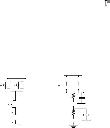
Propagation Delay of Complementary CMOS Gates
The computation of propagation delay proceeds in a fashion similar to the static inverter. For the purpose of delay analysis, each transistor is modeled as a resistor in series with an ideal switch. The value of the resistance is dependent on the power supply voltage and an equivalent large signal resistance, scaled by the ratio of device width over length, must be used. The logic is transformed into an equivalent RC network that includes the effect of internal node capacitances. Figure 6.8 shows the two-input NAND gate and its equivalent RC switch level model. Note that the internal node capacitance Cint —attributable to the source/drain regions and the gate overlap capacitance of M2/M1— is included. While complicating the analysis, the capacitance of the internal nodes can have quite an impact in some networks such as large fan-in gates.
VDD
A 
 B
B
M3 
 M4
M4

 F
F
A 

 M2
M2
B 

 M1
M1
(a) Two-input NAND
Figure 6.8 Equivalent RC model for a NAND gate.
VDD
 RP
RP  RP
RP
A  B
B


 F
F
RN
CL
B

RN
Cint
A 
(b) RC equivalent model
We will initially ignore the effect of the internal capacitance (for a first pass). The most important observation is that delay is also dependent on the input patterns. Consider for instance the low-to-high transition. Three possible input scenarios can be identified for charging the output to VDD. If both inputs are driven low, the two PMOS devices are on. The delay in this case is 0.69 × (Rp/2) × CL, since the two resistors are in parallel. This is not the worst-case low-to-high transition, which occurs when only one device turns on, and is given by 0.69 × Rp × CL. For the pull-down path, the output is discharged only if both A and B are switched high, and the delay is given by 0.69 × (2RN) × CL to a first order. In other words, adding devices in series slows down the circuit, and devices must be made wider to avoid a performance penalty. When sizing the transistors in a gate with multiple fan-in’s, we should pick the combination of inputs that triggers the worst-case conditions.
For example, for a NAND gate to have the same pull-down delay delay (tphl) as a minimum sized inverter (NMOS: 0.375μm/0.25μm and PMOS: 1.125μm/0.25μm), the
Section 6.2 Static CMOS Design |
205 |
NMOS devices in the NAND stack must be made twice as large (i.e., NMOS of NAND should be 0.75μm/0.25μm) so that the equivalent resistance the NAND pull-down is the same as the inverter. The PMOS device can remain unchanged.
This first-order analysis assumes that the extra capacitance introduced by widening the transistors can be ignored. This is not a good assumption in general, but allows for a reasonable first cut at device sizing.
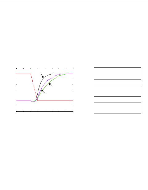
Example 6.3 Delay dependence on input patterns
Consider the NAND gate of Figure 6.8a. Assume NMOS and PMOS devices of 0.5μm/0.25μm and 0.75μm/0.25μm, respectively. This sizing should result in approximately equal worst-case rise and fall times (since the effective resistance of the pull-down is designed to be equal to the pull-up resistance).
Figure 6.9 shows the simulated low-to-high delay for different input patterns. As expected, the case where both inputs transition go low (A = B = 1→0) results in a smaller delay, compared to the case where only one input is driven low. Notice that the worst-case low-to-high delay depends upon which input (A or B) goes low. The reason for this involves the internal node capacitance of the pull-down stack (i.e., the source of M2). For the case that B = 1 and A transitions from 1→0, the pullup PMOS device only has to charge up the output node capacitance since M2 is turned off. On the other hand, for the case where A=1 and B transitions from 1→0, the pull-up PMOS device has to charge up the sum of the output and the internal node capacitances, which slows down the transition.
Voltage, V
3.0 |
|
|
|
|
|
|
Input Data |
Delay |
|
|
|
A = B = 1→0 |
|
|
|
||||
|
|
|
|
|
|
||||
|
|
|
|
|
|
|
Pattern |
(pS) |
|
2.0 |
|
|
|
|
|
|
A = B= 0→1 |
69 |
|
|
|
|
|
|
|
|
|||
1.0 |
|
|
A = 1, B = 1→0 |
|
A = 1, B= 0→1 |
62 |
|||
|
|
|
|
|
|||||
|
|
|
|
|
|
A= 0→1, B = 1 |
50 |
||
|
|
|
A = 1→0, B =1 |
|
|
||||
|
|
|
|
|
A=B=1→0 |
|
|||
0.0 |
|
|
|
|
|
|
35 |
||
|
|
|
|
|
|
A=1, B = 1→0 |
76 |
||
|
|
|
|
|
|
|
|||
|
|
|
|
|
|
|
A= 1→0, B = 1 |
57 |
|
-1.00 |
100 |
200 |
300 |
400 |
|||||
|
|
||||||||
|
|
||||||||
time, ps
Figure 6.9 Example showing the delay dependence on input patterns.
The table in Figure 6.9 shows a compilation of various delays for this circuit. The first-order transistor sizing indeed provides approximately equal rise and fall delays. An important point to note is that the high-to-low propagation delay depends on the state of the internal nodes. For example, when both inputs transition from 0→1, it is important to establish the state of the internal node. The worst-case happens when the internal node is charged up to VDD-VTn. The worst case can be ensured by pulsing the A input from 1 →0→1, while input B only makes the 0→1. In this way, the internal node is initialized properly.
The important point to take away from this example is that estimation of delay can be fairly complex, and requires a careful consideration of internal node capacitances and data patterns. Care must be taken to model the worst-case scenario in the simulations. A brute force approach that applies all possible input patterns, may not always work as it is important to consider the state of internal nodes.
206 |
DESIGNING COMBINATIONAL LOGIC GATES IN CMOS |
Chapter 6 |
The CMOS implementation of a NOR gate (F = A + B) is shown in Figure 6.10. The output of this network is high, if and only if both inputs A and B are low. The worst-case pull-down transition happens when only one of the NMOS devices turns on (i.e., if either A or B is high). Assume that the goal is to size the NOR gate such that it has approximately the same delay as an inverter with the following device sizes: NMOS 0.5μm/0.25μm and PMOS 1.5μm/0.25μm. Since the pull-down path in the worst case is a single device, the NMOS devices (M1 and M2) can have the same device widths as the NMOS device in the inverter. For the output to be pulled high, both devices must be turned on. Since the resistances add, the devices must be made two times larger compared to the PMOS in the inverter (i.e., M3 and M4 must have a size of 3μm/0.25μm). Since PMOS devices have a lower mobility relative to NMOS devices, stacking devices in series must be avoided as much as possible. A NAND implementation is clearly prefered over a NOR implementation for implementing generic logic.
|
|
|
|
|
V |
VDD |
|
|
||||||||
|
|
|
|
|
DD |
|
|
|
|
|
|
|
||||
|
|
|
|
|
|
|
|
|
|
RP |
|
|
||||
B |
|
M4 |
|
|
||||||||||||
|
B |
|
|
|
|
F |
||||||||||
|
|
|
|
|
|
|
|
|
|
|
|
|
||||
|
|
|
|
|
|
|
|
|
|
|||||||
|
|
|
|
|
|
|
|
|
|
|
|
|
|
|
||
A |
|
|
M3 |
RP |
|
|
C |
|||||||||
|
|
|
||||||||||||||
|
|
|
|
|
|
|
|
|
F |
A |
|
|
|
|
|
int |
|
|
|
|
|
|
|
|
|
|
|
|
|
F |
|||
|
|
|
|
|
|
|
|
|
|
|||||||
|
|
|
|
|
|
|
|
|
|
|
|
|
|
|
|
|
A |
|
M1 |
B |
|
M2 |
|
|
|
|
|
||||||
|
|
RN |
RN |
|
||||||||||||
|
|
|
CL |
|||||||||||||
|
|
|
|
|
|
|
|
|
A |
|
||||||
|
|
|
|
|
|
|
|
|
|
B |
|
|
||||
|
|
|
|
|
|
|
|
|
|
|
|
|
|
|
|
|
Figure 6.10Sizing of a NOR gate to produce the same delay as an inverter with size of NMOS: 0.5μm/0.25μm and PMOS: 1.5μm/0.25μm.
Problem 6.1 Transistor Sizing in Complementary CMOS Gates
Determine the transistor sizes of the individual transistors in Figure 6.6c such that it has approximately the same tplh and tphl as a inverter with the following sizes: NMOS: 0.5μm/0.25μm and PMOS: 1.5μm/0.25μm.
So far in the analysis of propagation delay, we have ignored the effect of internal node capacitances. This is often a reasonable assumption for a first-order analysis. However, in more complex logic gates that have large fan-in, the internal node capacitances can become significant. Consider a 4-input NAND gate as shown in Figure 6.11, which shows the equivalent RC model of the gate, including the internal node capacitances. The internal capacitances consist of the junction capacitance of the transistors, as well as the gate-to-source and gate-to-drain capacitances. The latter are turned into capacitances to ground using the Miller equivalence. The delay analysis for such a circuit involves solving distributed RC networks, a problem we already encountered when analyzing the delay of interconnect networks. Consider the pull-down delay of the circuit. The output is discharged when all inputs are driven high. The proper initial conditions must be placed on the internal nodes (this is, the internal nodes must be charged to VDD-VTN) before the inputs are driven high.