

Section 6.3 Dynamic CMOS Design |
237 |
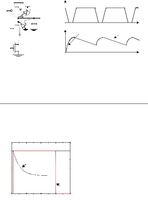
Obviously, the number of switches per segment grows with increasing values of tbuf. In current technologies, mopt typically around 3.
m
Req |
|
Req |
|
|
Req |
Req |
Req |
Req |
||||
In |
|
C |
|
C C |
|
C |
|
C |
|
C C |
|
C |
|
|
|
|
|
|
|||||||
|
|
|
|
|
|
|
||||||
|
|
|
|
|
|
|||||||
|
|
|
|
|
|
|||||||
|
|
|
|
|
|
|
|
|
|
|
|
|
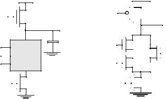
Figure 6.47Breaking up long transmission gate chains by inserting buffers.
Example 6.12 Transmission Gate Chain
Consider the same 16 transmission gate chain. The buffers shown in Figure 6.47 can be implemented as inverters (instead of two cascaded inverters). In some cases, it might be necessay to add an extra inverter to produce the correct polarity. Assuming that each inverter is sized such that the NMOS is 0.5μm/0.25μm and PMOS is 0.5μm /0.25μm, Eq. (6.28) predicts that an inverter must be inserted every 3 transmission gates. The simulated delay when placing an inverter every two transmission gates equals 154ps, for every three transmission gates is 154ps and for four transmission gates is 164ps. The insertion of buffering inverters reduces the delay with a factor of almost 2.
CAUTION: Although many of the circuit styles discussed in the previous sections sound very exciting, and might be superior to static CMOS in many respects, none of them has the robustness and ease of design of complementary CMOS. Therefore, use them sparingly and with caution. For designs that have no extreme area, complexity, or speed constraints, complementary CMOS is the recommended design style.
6.3Dynamic CMOS Design
It was noted earlier that static CMOS logic with a fan-in of N requires 2N devices. A variety of approaches were presented to reduce the number of transistors required to implement a given logic function including pseudo-NMOS, pass transistor logic, etc. The pseudo-NMOS logic style requires only N + 1 transistors to implement an N input logic gate, but unfortunately it has static power dissipation. In this section, an alternate logic style called dynamic logic is presented that obtains a similar result, while avoiding static power consumption. With the addition of a clock input, it uses a sequence of precharge and conditional evaluation phases to realize complex logic functions.
238 |
DESIGNING COMBINATIONAL LOGIC GATES IN CMOS |
Chapter 6 |
6.3.1Dynamic Logic: Basic Principles
The basic construction of a N-type dynamic logic gate is shown in Figure 6.48a. The PDN (pull-down network) is constructed exactly in the same fashion as a complementary CMOS. The operation of this circuit can be divided into two major phases: precharge and evaluation, with the mode of operation determined by the clock signal.
VDD |
VDD |
CLK
 Mp
Mp
Out
CL
In1
In2  PDN
PDN
In3
CLK Me
Me
(a) N-type network
Figure 6.48 Basic concepts of a dynamic gate.
|
|
|
|
|
|
|
|
CLK |
|
Mp |
|
|
|
|
|
|
|
|
|
Out
A


 C B
C B 

CLK 
 Me
Me
(b) Example
Precharge
When CLK = 0, the output node Out is precharged to VDD by the PMOS transistor Mp. During that time, the evaluate NMOS transistor Me is off, so the pull-down path does not fight the pull-up path. The evaluation FETS also eliminate any static power that would be consumed during the precharge period (i.e., if the pull-down path was turned on and the precharge device was turned on, static current would flow between the supplies).
Evaluation
When CLK = 1, the precharge transistor Mp is off, and the evaluation transistor Me is turned on. The output is conditionally discharged based on the input values and the pulldown topology. If the inputs are such that the PDN conducts, then a low resistance path exists between Out and GND and the output is discharged to GND. If the PDN is turned off, the precharged value remains stored on the output capacitance CL, which is a combination of junction capacitances, the wiring capacitance, and the input capacitance of the fanout gates. During the evaluation phase, the only possible path between the output node and a supply rail is to GND. Consequently, once Out is discharged, it cannot be charged again till then next precharge operation. The inputs to the gate can therefore make at most one transition during evaluation. Notice that the output can be in the high impedance state during the evaluation period if the pull-down network is turned off and this behavior is fundamentally different than the static counterpart that always has a low resistance path between the output and one of the power rails.

Section 6.3 Dynamic CMOS Design |
239 |
As as an example of dynamic logic, consider the circuit shown in Figure 6.48b. During the precharge phase (CLK=0), the output is precharged to VDD regardless of the input values since the evaluation device is turned off. During evaluation (CLK=1), a conducting path is created between Out and GND if (and only if) A·B+C is TRUE. Otherwise, the output remains at the precharged state of VDD. The following function is thus realized:
Out = A × B + C (when CLK = 1) |
(6.29) |
A number of important properties can be derived for the dynamic logic gate:
•The logic function is implemented by the NMOS pull-down network. The construction of the PDN proceeds just as it does for static CMOS.
•The number of transistors (for complex gates) is substantially lower than in the static case: N + 2 versus 2N.
•It is nonratioed. The sizing of the PMOS precharge device is not important for realizing proper functionality of the gate. The size of the precharge device can be made large to improve the low-to-high transition time (of course, at a cost to the high-to- low transition time). There is however, a trade-off with power dissipation since a larger precharge device directly increases clock power dissipation.
•It only consumes dynamic power. Ideally, no static current path ever exists between
VDD and GND. The overall power dissipation, however, can be significantly higher compared to a static logic gate.
•The logic gates have faster switching speeds. There are two main reasons for this. The first (obvious) reason is due to the reduced load capacitance attributed to the number of transistors per gate and the single-transistor load per fan-in. Second, the dynamic gate do not have short circuit current, and all the current provided by the pull-down devices go into discharging the load capacitance.
The low and high output levels VOL and VOH are easily identified as GND and VDD and are not dependent upon the transistor sizes. The other VTC parameters are dramatically different from static gates. Noise margins and switching thresholds have been defined as static quantities, which are not influenced by time. To be functional, a dynamic gate requires a periodic sequence of precharges and refreshes. Pure static analysis, therefore, does not apply. During the evaluate period, the pull-down network of a dynamic inverter starts to conduct when the input signal exceeds the threshold voltage (VTn) of the NMOS pull-down transistor. Therefore, it is reasonable to set the switching threshold (VM) as well as VIH and VIL of the gate equal to VTn. This translates to a low value for the NML.
6.3.2Speed and Power Dissipation of Dynamic Logic
The main advantage of dynamic logic is speed and potentially smaller implementation area. Fewer devices to implement a given logic function implies that the overall load capacitance is much smaller. The analysis of the switching behavior of the gate has some interesting peculiarities to it. After the precharge phase, the output is high. For a low input signal, no additional switching occurs. As a result, tpLH = 0! The high-to-low transition, on
240 |
DESIGNING COMBINATIONAL LOGIC GATES IN CMOS |
Chapter 6 |
VDD
CLK 


Out
In1
In2
In3
In4
CLK
Voltage
2.5 
Out
1.5 
IN &
CLK
0.5 
-0.5 0 |
0.5 |
1 |
Time, ns
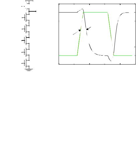
Figure 6.49Schematic of a dynamic four-input NAND gate.
the other hand, requires the discharging of the output capacitance through the pull-down network. Therefore tpHL is proportional to CL and the current-sinking capabilities of the PDN. The presence of the evaluation transistor slows the gate somewhat, as it presents an extra series resistance to the pull-down network. Omitting this transistor, while functionally not forbidden, results in significant performance loss and static power dissipation.
The above analysis is somewhat unfair, because it ignores the influence of the precharge time on the switching speed of the gate. The precharge time is determined by the time it takes to charge CL through the PMOS precharge transistor. During this time, the logic in the gate cannot be utilized. However, very often, the overall digital system can be designed in such a way that the precharge time coincides with other system functions. For instance, the precharge of the arithmetic unit in a microprocessor can coincide with the instruction decode. The designer has to be aware of this “dead zone” in the use of dynamic logic, and should carefully consider the pros and cons of its usage, taking the overall system requirements into account.
Example 6.13 A Four-Input Dynamic NAND Gate
Figure 6.49 shows the design of a four-input NAND example designed using the dynamic-cir- cuit style. Due to the dynamic nature of the gate, the derivation of the voltage-transfer characteristic diverges from the traditional approach. As we had discussed above, we will assume that the switching threshold of the gate equals the threshold of the NMOS pull-down transistor. This results in asymmetrical noise margins, as shown in Table 6.7.
The dynamic behavior of the gate is simulated with SPICE. It is assumed that all inputs are set high as the clock transitions high. On the rising edge of the clock, the output node is discharged. The resulting transient response is plotted in Figure 4.35. The resulting propagation delays are summarized in Table 6.7. The length of the precharge time can be adjusted by changing the size of the PMOS precharge transistor. Making the PMOS too large should be avoided, however, as it both slows down the gate and increases the capacitive load on the clock line. For large designs, the latter factor might become a major design concern because the clock load can become excessive and hard to drive.
Section 6.3 Dynamic CMOS Design |
241 |
Table 6.7 The dc and ac parameters of a four-input dynamic NAND.
Transistors |
VOH |
VOL |
VM |
NMH |
NML |
tpHL |
tpLH |
tpre |
6 |
2.5 V |
0 V |
VTN |
2.5- |
VTN |
110 ps |
0 nsec |
83pS |
|
|
|
|
VTN |
|
|
|
|
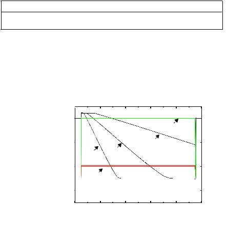
As mentioned earlier, the static parameters are time dependent. To illustrate this, consider the four input NAND gate with all inputs tied together. Assume that the inputs make a partial low-to-high transition. Figure 6.50 shows a simulation of the output voltage for three different input voltages (when input transitions to 0.45V, 0.5V and 0.55V). We have previously defined the switching threshold of the dynamic gate as the device threshold. However, notice that the amount by which the output voltage drops is a strong function of the input voltage and the available evaluation time. In this example, a larger input voltage is necessary to corrupt the output. So the switching threshold is really a function of the evaluation time.
Voltage, V
3.0 
CLK
2.0 
|
|
|
Vout |
|
Vout |
Vout |
(VG=0.45) |
1.0 |
(VG=0.5) |
|
|
(VG=0.55) |
|
||
0.0 |
VG |
|
|
|
|
|
-1.0 0 |
20 |
40 |
60 |
80 |
100 |
Time, ns
Figure 6.50Effect of an input glitch on the output. The switching threshold depends on the time for evaluation. A larger glitch is acceptable if the evaluation phase is smaller. In this example, the input glitches high during evaluation and stays high during the whole period.
When evaluating the power dissipation of a dynamic gate, it would appear that dynamic logic presents significant advantage. There are three reasons for this. First, since dynamic logic uses fewer transistors to implement a given function, it should have a lower physical capacitance. Basically the load seen for each fanout is one transistor instead of two. Second, dynamic logic gates by construction can at most have one transition per clock cycle. The glitching transitions seen in static gates are not seen in dynamic gates. Finally, dynamic gates do not exhibit short circuit power since the pull-up path is not turned on when the gate is evaluating. While the above statements are generally true, several important second order effects causes the number of transistors to be higher than the minimal set required for implementing the logic and short circuit power does exist if the logic is required to be pseudo-static. Also, the clock power of dynamic logic can be significant particularly since the clock node has a guaranteed transition on every single clock cycle.

242 |
DESIGNING COMBINATIONAL LOGIC GATES IN CMOS |
Chapter 6 |
Dynamic logic generally has higher activity due to constant precharge and discharge operations. Earlier, the transition probability for a static gate was shown to be p0 p1 = p0 (1-p0). For dynamic logic, the output transition probability does not depend on the state (history) of the inputs but rather on just the signal probabilities. For an N-tree dynamic gate, the output will make a 0 to 1 transition during the precharge phase only if the output was discharged by the N-tree logic during the evaluate phase. The zero to one transition probability for an N-tree structure is therefore
α0 → 1 = p0 |
(6.30) |
where p0 is the probability that the output is in the zero state. For uniformly distributed inputs, this means that the transition probability is:
N0 |
(6.31) |
α0 → 1 = ------ |
|
2N |
|
where N0 is the number of zero entries in the truth table of the logic function.
Example 6.14Activity estimation in dynamic logic
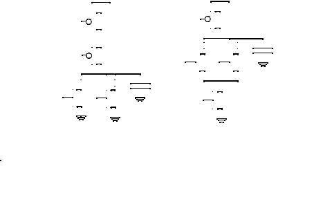
To illustrate the increased activity for a dynamic gate, once again consider a 2 input NOR gate. An N-tree dynamic NOR gate is shown in Figure 6.51 along with its static counterpart. For the dynamic implementation, power is consumed during the precharge operation for the times when the output capacitor was discharged the previous cycle. For equi-probable input, there is then a 75% probability that the output node will discharge immediately after the precharge phase, implying that the activity for such a gate is 0.75 (i.e PNOR= 0.75 CLVdd2fclk). The corresponding activity is a lot smaller, 3/16, for a static implementation. Note that for the dynamic case, the activity depends only on the signal probability, while for the static case the transition probability depends on previous state. If the inputs to a static CMOS gate do not change from the previous sample period, then the gate does not switch. This is not true in the case of dynamic logic in which gates can switch. For a dynamic NAND gate, the transition probability is 1/4 (since there is a 25% probability the output will be discharged) while it is 3/16 for a static implementation. Though this example illustrates that the switching activity can be higher using dynamic
Section 6.3 Dynamic CMOS Design |
243 |
logic, it should be noted that dynamic logic has lower physical capacitance. Both factors must be accounted for when choosing a logic style.
|
|
|
|
|
VDD |
|
|
|
|
|
VDD |
|||||||||||||||
|
A |
|
|
|
|
|
|
|
|
|
|
CLK |
|
|
|
|
|
|
|
|
|
|||||
|
|
|
|
|
|
|
|
|
|
|
|
|
||||||||||||||
|
|
|
|
|
|
|
|
|
|
|
|
|
|
|
|
|
|
|||||||||
|
|
|
|
|
|
|
|
|
|
|
|
|
|
|
|
|
|
|
|
|
|
|
|
|
|
CL |
|
B |
|
|
|
|
|
|
|
|
|
|
|
|
|
|
|
|
|
|
|
|
|
||||
|
|
|
|
|
|
|
|
|
|
|
|
|
|
B |
|
|
|
|||||||||
|
|
|
|
|
|
|
|
|
|
|
|
|
|
|
|
|
||||||||||
|
|
|
|
|
|
|
|
|
|
|
|
|
A |
|
|
|
|
|
|
|
|
|||||
|
|
|
|
|
||||||||||||||||||||||
A |
|
|
|
|
|
|
|
|
|
|
|
|
CL |
|
|
|
|
|
|
|
|
|
|
|
|
|
|
|
B |
|
|
|
|
|
|
|
|
|
|
|
|
|
|
|
|
|
|
||||||
|
|
|
|
|
|
|
CLK |
|
|
|
|
|
|
|
|
|||||||||||
|
|
|
|
|
|
|
|
|
|
|
|
|
|
|
||||||||||||
|
|
|
|
|
|
|
|
|
|
|
||||||||||||||||
|
|
|
|
|
|
|
|
|
|
|
|
|
|
|
|
|
|
|||||||||
|
|
|
|
|
|
|
|
|
|
|
|
|
|
|
|
|
|
|
|
|
|
|
|
|
|
|
|
|
|
|
|
|
|
|
|
|
|
|
|
|
|
|
|
|
|
|
|
|
|
|
|
|
|
|
|
|
|
|
|
|
|
|
|
|
|
|
|
|
|
|
|
|
|
|
|
|
|
|
|
|
Figure 6.51Static NOR vs. N-tree based dynamic NOR.
Problem 6.7 Activity Computation
For the 4-input dynamic NAND gate, compute the activity factor with the following assumption for the inputs. Assume that the inputs are independent and pA=1 = 0.2, pB=1 = 0.3, pC=1 = 0.5, and pD=1 = 0.4.
6.3.3Issues in Dynamic Design
Dynamic logic clearly can result in high performance solutions compared to static circuits. However, there are several important considerations that must be taken into account to make dynamic circuits function properly. This include charge leakage, charge sharing, backgate (and in general capacitive) coupling, and clock feedthrough. Some of these issues are highlighted in this section.
Charge Leakage
The operation of a dynamic gate relies on the dynamic storage of the output value on a capacitor. During the evaluation period, if the pull-down network is off, then ideally the output should remain at the precharged state of VDD. However, due to leakage currents, this charge gradually leaks away, resulting eventually in malfunctioning of the gate. Figure 6.52a shows the different sources of leakage for a simple dynamic inverter circuit.
Source 1 and 2 are the reverse-biased diode and sub-threshold leakage of the NMOS pull-down device M1 respectively. The charge stored on CL will slowly leak away due these leakage sources, assuming that the input is in the low state during evaluation. Charge leakage causes a degradation in the high level (Figure 6.52b). Dynamic circuits therefore require a minimal clock rate, which is typically on the order of a few kHz. This makes the usage of dynamic techniques unattractive for certain low performance products such as watches or processors that need to provide conditional clocks (where there are no
244 |
|
|
|
|
|
|
|
DESIGNING COMBINATIONAL LOGIC GATES IN CMOS |
Chapter 6 |
|||
|
|
|
VDD |
|
|
|
CLK |
|
|
|
||
CLK |
|
|
|
|
(4) |
|
|
|
|
|
|
|
|
|
|
|
|
|
|
|
|
|
|
||
|
|
|
|
|
|
|
|
|
||||
|
|
Mp |
|
|
(3) |
|
|
|
||||
|
|
|
|
|
|
|
|
|||||
|
|
|
|
|
|
(1) |
|
Out |
|
|
|
|
|
|
|
|
|
|
|
|
|
||||
|
|
|
|
|
|
|
|
|
|
|||
A = 0 |
|
|
|
|
|
CL |
|
|
t |
|||
|
M1 |
|
|
|
|
|
||||||
|
|
|
|
|
|
Vout |
Precharge |
Evaluate |
|
|||
|
|
|
|
(2) |
|
|
|
|
||||
|
|
|
|
|
|
|
||||||
|
|
|
|
|
|
|
|
|
|
|
|
|
CLK
Me
t
(a) Leakage sources (b) Effect on waveforms
Figure 6.52 Leakage issues in dynamic circuits.
guarantees on minimum clock rates). Note that the PMOS precharge device also contributes some leakage due the reverse bias diode (source 3) and subthreshold conduction (source 4). To some extent, the leakage current of the PMOS counteracts the leakage due to the pull-down path. As a result the output voltage is going to be set by the resistive divider composed of the pull-down and pull-up paths.
Example 6.15Example of leakage
Consider the simple inverter with all devices set at 0.5μm/0.25μm. Assume that the input is low during the evaluation period. Ideally, the output should remain at the precharged state of VDD. However, as seen from Figure 6.53 the output voltage drops. Once the output drops below the switching threshold of the fan-out logic gate, the output is interpreted as a low voltage. Notice that the output settles to an intermediate voltage. This is due to the leakage provided by the PMOS pull up device.
3.0 
2.0 
VVoltage,
1.0 
0.00
Out
|
|
|
CLK |
10 |
20 |
30 |
40 |
|
time, ms |
|
|
Figure 6.53 Impact of charge leakage. The output settles to an intermediate voltage determined by a resistive divider of the pulldown and pull up devices.
Leakage is caused by the high impedance state of the output node when the pull down path is turned off during the evaluate mode. To deal with the leakage problem, the impedance on the output node must be reduced during evaluate period. This is often done
Section 6.3 Dynamic CMOS Design |
245 |
by adding a bleeder transistor to the output node, as shown in Figure 6.54. The bleeder compensates for the charge lost due to the pull-down leakage paths. When the clock is high and the pull-down network is turned off, the output remains high. In order to avoid the ratioed problems associated with this circuit, the bleeder resistance is made high (small device size). This allows the pull-down devices has to be strong enough to pull-down the Out node below the switching threshold of the inverter. The circuit does have static power dissipation when Out is pulled low during the evaluation period. Often, the bleeder is implemented in a feedback configuration to eliminate static power dissipation.
|
|
VDD |
||||||
|
|
|
|
|
|
|
|
|
|
|
|
|
|
|
|
|
|
CLK |
|
Mp |
Mbl |
|
|
|
||
|
|
|
|
|||||
|
|
|
|
|
|
|
|
|
|
|
|
|
|
|
|
|
|
|
|
|
|
|
|
|
|
|
Out
A 
 Ma
Ma
B 
 Mb
Mb
CLK 
 Me
Me
Figure 6.54Static bleeder to compensate for the charge leakage problem.
Charge Sharing
Another important consideration in dynamic logic is charge sharing. Consider the circuit of Figure 6.55. During the precharge phase, the output node is precharged to VDD. Assume that all inputs are set to 0 during precharge and that the capacitance Ca is discharged. Assume further that input B remains at 0 during evaluation, while input A makes a 0 → 1 transition, turning transistor Ma on. The charge stored originally on capacitor CL is redistributed over CL and Ca. This causes a drop in the output voltage, which cannot be recovered due to the dynamic nature of the circuit.
The influence on the output voltage is readily calculated. Under the above assump-
tions, the following initial conditions are valid: Vout(t = 0) = VDD and VX(t = 0) = 0. Two cases must be considered:
1. |
Vout < VTn—In this case, the final value of VX equals VDD – VTn(VX). Charge conser- |
|
|
vation yields |
|
|
CLVDD = CLVout(t) + Ca[VDD – VTn(VX )] |
|
|
or |
(6.32) |
|
Ca |
|
|
(VX )] |
|
|
Vout = Vout(t) – VDD = –-----[VDD – VTn |
|
|
CL |
|
2. |
Vout > VTn—Vout and VX reach the same value: |
|
246 |
|
|
|
|
|
|
|
|
DESIGNING COMBINATIONAL LOGIC GATES IN CMOS |
Chapter 6 |
|
|
VDD |
|
|
|
|||||
|
|
|
|
|
|
|
|
|
|
|
|
|
|
|
|
|
|
|
|
|
|
CLK |
|
Mp |
|
|
|
|||||
|
|
|
|
|
|
|
|
|
Out |
|
|
|
|
|
|
|
|
|
|
||
|
|
|
|
|
|
|
|
|
||
|
|
|
|
|
|
|
|
|
CL |
|
|
|
|
|
|
|
|
|
|
|
|
A |
|
Ma |
|
|
|
|||||
|
|
|
|
|||||||
|
|
|
X |
|
Ca |
|
||||
|
|
|
|
|
||||||
|
|
|
|
|
|
|
|
|
|
|
|
|
|
|
|
|
|
|
|
|
|
B = 0 |
|
Mb |
|
|
|
|
|
|
||
|
|
|
|
|
|
Cb |
|
|||
|
|
|
|
|
||||||
CLK |
|
|
|
|
|
|
|
|
|
|
|
|
|
|
|
|
|
|
|
||
|
|
|
|
|
|
|
|
|
||
|
|
|
|
|
|
|
|
|||
|
Me |
|
|
|
|
|
||||
|
|
|
|
Figure 6.55 Charge sharing in dynamic networks. |
|
|||||
|
|
|
|
|||||||
|
|
|
|
|
|
|
|
|
|
|
|
|
|
|
|
|
|
|
|
|
|
DV |
|
= –V |
|
Ca |
(6.33) |
|
æ------------------ö |
||||
|
out |
|
DD èCa |
+ CLø |
|
Overall, it is desirable to keep the value of DVout below |VTp|. The output of the dynamic gate might be connected to a static inverter, in which case the low level of Vout would
cause static power consumption. One major concern is circuit malfunction if the output voltage is brought below the switching threshold of the gate it drives.
Example 6.16 Charge Sharing Example
Consider the dynamic logic gate shown in Figure 6.56. It can be easily verified that the function implemented by the logic gate is y = A Å B Å C. To analyze charge sharing, the question we will ask is for the case when the output is nominally supposed to stay high, what is the worst case change in voltage on node y. For simplicity, ignore the load inverter, and assume that all inputs are low during the precharge operation and that all isolated internal nodes (Va, Vb, Vc, and Vd) are initially at 0V.
|
|
|
|
|
|
|
|
|
VDD = 2.5V |
|
|
|
|
|
||||||||||
|
|
|
|
|
|
|
CLK |
|
|
|
|
|
|
|
|
|
|
|
|
|
|
Load Inverter |
||
|
|
|
|
|
|
|
|
|
|
|
||||||||||||||
|
|
|
|
|
|
|
|
|
|
|
|
|
|
|
|
|
|
|
|
y |
||||
|
|
|
|
|
|
|
|
|
|
|
|
|
|
|
|
|
|
|
|
|||||
|
|
|
|
|
|
|
A |
|
|
A |
|
|
|
|
|
Cy = 50 fF |
||||||||
|
|
|
|
|
|
|
|
|
|
|
|
|
|
|||||||||||
Ca = 15 fF |
|
|
a |
|
|
|
|
|
|
|
|
|
|
|
||||||||||
|
|
|
|
|
|
|
|
|
|
|
|
|||||||||||||
|
|
|
|
|
|
|
|
|
|
|
|
|
|
|
|
|
|
|||||||
|
|
|
|
|
|
|
|
|
|
|
|
|
|
|
|
|
|
|
|
|
||||
|
|
|
|
|
|
|
|
|
|
|
|
|
b |
|
B |
|
|
|
|
Cb = 15 fF |
||||
B |
|
|
|
|
|
B |
|
|
B |
|
|
|
|
|
|
|
|
|||||||
|
|
|
|
|
|
|
|
|
|
|
|
|
|
|
|
|
||||||||
|
|
|
c |
|
|
|
|
|
|
|
|
|
|
|
|
|
|
|
|
|
d |
|||
|
|
|
|
|
|
|
|
|
|
|
|
|
|
|
||||||||||
Cc = 15 fF |
|
|
|
|
|
|
C |
|
|
|
|
|
|
|
|
Cd = 10 fF |
||||||||
|
|
|
|
|
|
|
|
|
|
|
|
|
|
|
||||||||||
|
|
|
|
|
|
|
C |
|
|
|
|
|
|
|
|
|
|
|
|
|
||||
|
|
|
|
|
|
|
|
|
|
|
|
|
|
|
|
|
|
|
|
|
|
|
|
|
CLK 

Figure 6.56Example illustrating the charge sharing effect in dynamic logic.