

Section 6.2 Static CMOS Design |
227 |
the availability of both polarities of every signal eliminates the need for extra inverters, as is often the case in static CMOS or pseudo-NMOS.
•CPL belongs to the class of static gates, because the output-defining nodes are
always connected to either VDD or GND through a low resistance path. This is advantageous for the noise resilience.
•The design is very modular. In effect, all gates use exactly the same topology. Only the inputs are permutated. This makes the design of a library of gates very simple. More complex gates can be built by cascading the standard pass-transistor modules.
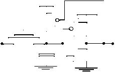
Example 6.9 Four-input NAND in CPL
Consider the implementation of a four-input AND/NAND gate using CPL. Based on the associativity of the boolean AND operation [A·B·C·D = (A·B)·(C·D)], a two-stage approach has been adopted to implement the gate (Figure 6.34). The total number of transistors in the gate
|
|
|
|
|
B |
|
B |
|
|
|
|
|
|
|
|
|
|||||||||||
B |
A |
Out |
C |
D |
A |
|
|
|
|
|
|
|
|
|
|
|
|
|
|
|
|
|
|
|
|
|
|
|
|
|
|
|
|
|
|
|
|
|
|
|
|
|
|
|
|
|
|
|
|||||||
|
|
|
|
|
|
|
|
|
|
|
|
|
|
|
|
|
|
|
|
|
|||||||
|
X |
|
Y |
|
B |
|
|
|
|
|
X |
|
X |
|
X |
||||||||||||
|
|
|
|
|
|
|
|
||||||||||||||||||||
|
|
|
A |
|
|
|
|
|
|
|
|
|
|
|
|
|
|
|
|||||||||
|
|
|
|
|
|
|
|
|
|
|
|
|
|
|
X Y |
|
|
|
|
|
|
|
|
|
|||
|
|
|
|
|
B |
|
|
|
|
|
|
|
|
|
|
|
|
Out |
|||||||||
|
|
|
|
|
|
|
|
|
|
|
|
|
|
|
|
|
|||||||||||
|
|
|
|
|
|
|
|
|
|
|
|
|
|
|
|
|
|||||||||||
|
|
|
|
|
|
|
|
|
D |
|
|
|
|
X |
|
|
|
|
|
|
|
|
|||||
|
|
|
|
|
|
|
|
|
|
|
|
|
|
|
|
|
|
|
|
||||||||
|
|
|
|
|
|
|
|
|
|
D |
|
|
|
|
|
|
|
|
|
||||||||
|
|
|
|
|
|
|
|
|
|
|
|
|
|
|
|
|
|
|
|||||||||
|
X |
|
Y |
|
|
|
|
|
|
|
|
|
|
|
|
|
|
Y |
|
|
|
|
|
|
|
|
|
|
|
|
|
|
C |
|
|
|
|
|
|
|
|
|
|
|
X |
|
|
|
|
|
|
|
|
Out |
|
|
|
|
|
|
|
|
|
|
|
|
|
|
|
|
|
|
|
|
|
|
|||||||
|
|
|
|
|
D |
|
|
|
|
|
Y |
|
|
|
|
|
|
|
|
|
|||||||
|
|
|
|
|
|
|
|
|
|
|
|
|
|
|
|
|
|
||||||||||
|
|
|
|
|
|
|
|
|
|
|
|
|
|
|
|
|
|
||||||||||
B |
A |
Out |
C |
D |
C |
|
|
|
|
|
|
|
|
|
|
|
|
|
|
|
|
|
|
||||
|
|
|
|
|
|
|
|
|
|
|
|
|
|
|
|
|
|
|
|
|
|
||||||
D |
|
|
|
|
Y |
|
|
|
|
|
|
|
|
|
|||||||||||||
|
|
|
|
|
|
|
|
|
|
|
|
|
|
|
|
|
|
||||||||||
|
|
|
|
|
|
|
|
|
|
|
|
|
|
|
|
|
|
||||||||||
Figure 6.34 Layout and schematics of four-input NAND-gate using CPL (the final inverter stage is omitted). See also Colorplate 9.
(including the final buffer) is 14. This is substantially higher than previously discussed gates. This factor, combined with the complicated routing requirements, makes this circuit style not particularly efficient for this gate. One should, however, be aware of the fact that the structure simultaneously implements the AND and the NAND functions, which might reduce the transistor count of the overall circuit.
In summary, CPL is a conceptually simple and modular logic style. Its applicability depends strongly upon the logic function to be implemented. The availability of a simple XOR as well of the ease of implementing some specific gate structures makes it attractive for structures such as adders and multipliers. Some extremely fast and efficient implementations have been reported in that application domain [Yano90]. When considering CPL, the designer should not ignore the implicit routing overhead of the complementary signals, which is apparent in the layout of Figure 6.34.
228 |
DESIGNING COMBINATIONAL LOGIC GATES IN CMOS |
Chapter 6 |
Robust and Efficient Pass-Transistor Design
Unfortunately, differential pass transistor logic, like single-ended pass transistor logic suffers from static power dissipation since the high input to the inverter only charges up to VDD-VTn. Static power is highly undesirable since in many portable electronics, the devices are idle for extended periods of time. Therefore, the voltage drop of pass transistors that causes lower noise margins and static power is not acceptable. There are several solutions proposed to deal with this problem as outlined below.
Solution 1: Level Restoration
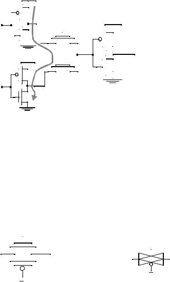
A common solution to the voltage drop of pass transistors is the use of a level restorer, which is a single PMOS configured in a feedback path (Figure 6.35). The gate of the PMOS device is connected to the output of the inverter, its drain connected to the input of the inverter and the source to VDD. Assume that node X is at 0V (out is at VDD and the Mr is turned off) with B = VDD and A = 0. If input A makes a 0 to VDD transition, Mn only charges up node X to VDD-VTn. This is, however, enough to switch the output of the inverter low, turning on the feedback device Mr and pulling node X all the way to VDD. This eliminates any static power dissipation in the inverter. Furthermore, no static current path can exist through the level restorer and the pass-transistor, since the restorer is only active when A is high. In summary, this circuit has the advantage that all voltage levels are either at GND or VDD, and no static power is consumed.
|
Level restorer |
VDD |
|
|
|
|
|
|
|
||||||
|
|
|
|
|
|
|
|
|
VDD |
|
|||||
|
|
B |
Mr |
|
|
|
|
|
|
|
|
||||
|
|
|
|
|
|
|
|
|
|
||||||
|
|
|
|
|
|
|
|
|
|
|
|
||||
|
|
|
|
|
|
|
|
|
|||||||
|
|
|
|
|
|
|
|
|
|||||||
|
|
|
|
|
|
|
|
|
|
M2 |
Out |
||||
|
|
|
|
|
|
|
|
|
|
|
|
|
|||
|
|
|
|
|
|
|
|
|
|
|
|
|
|||
|
|
|
|
|
|
X |
|
|
|
|
|
|
|||
A |
|
Mn |
|
|
|
|
|
|
|
|
|
|
|
|
|
|
|
|
|
|
|
|
|
|
|
|
|
|
|||
|
|
|
|
|
|
|
|
|
|
|
|
|
|
|
|
|
|
|
|
|
|
|
|
|
|
|
|
|
M1 |
||
|
|
|
|
|
|
|
|
|
|||||||
|
|
|
|
|
|
|
|
|
|
|
|
|
|||
|
|
|
|
|
|
|
|
|
|
|
|
|
|
|
|
|
|
|
|
|
|
|
|
|
|
|
|
|
|
|
|
|
|
|
|
|
|
|
|
|
|
|
|
|
|
|
|
Figure 6.35 Level-restoring circuit.
While this solution is appealing in terms of eliminating static power dissipation, it is more complex since the circuit is now ratioed. The problem arises during the transition of node X from high-to-low. The pass transistor network attempts to pull-down node X while the level restorer pulls now X to VDD. Therefore, the pull-down device must be stronger than the pull-up device to switch node X and the output. We use the notation R1 to denote the equivalent on-resistance of transistor M1, R2 for M2, and so on. Some careful transistor sizing is necessary to make the circuit function correctly: when Rr is made too small, it is impossible to bring the voltage at node X below the switching threshold of the inverter. Hence, the inverter output never switches to VDD, and the level-restoring transistor stays on. This sizing problem can be reformulated in the following way:
The resistance of Mn and Mr must be such that the voltage at node X drops below the threshold of the inverter, VM = f(R1, R2). This condition is sufficient to guarantee a switching of the output voltage Vout to VDD and a turning off of the level-restoring transistor.
Section 6.2 |
Static CMOS Design |
|
|
|
|
|
|
|
|
|
|
|
|
|
229 |
|
|
|
|
|
|
VDD |
|
|
|
||||||||
|
|
|
|
|
|
|
|
|||||||||
|
|
|
|
|
|
|
|
|
|
|
|
|
|
VDD |
|
|
|
|
|
|
|
|
|
|
|
|
|
|
|
|
|
||
|
|
|
|
|
|
|
|
|
|
|
|
|
|
|
||
|
|
|
B |
Mr |
|
|
|
|
|
|
|
|
|
|||
|
|
|
|
|
|
|
||||||||||
|
|
|
|
|
|
|
|
|||||||||
|
|
|
|
|
|
|
|
|
|
|
|
M2 |
|
|||
|
|
|
|
|
|
|
X |
|
|
|
|
|
|
|||
|
|
|
|
|
|
|||||||||||
|
|
|
|
|
|
|
|
|
|
|
|
|
|
|||
|
A = 0 |
|
Mn |
|
|
Out |
||||||||||
|
|
|
|
|
|
|
|
|
|
|
|
|
||||
|
|
|
|
|
|
|
|
|
|
|
|
|
|
M1 |
Figure 6.36 Transistor-sizing problem |
|
|
|
|
|
|
|
|
|
|
|
|
|
|
|
|||
|
|
|
|
|
|
|
|
|
|
|
|
|
|
for level-restoring circuit. |
||
|
|
|
|
|
|
|
|
|
|
|
|
|
|
|
|
|
|
|
|
|
|
|
|
|
|
|
|
|
|
|
|
|
|
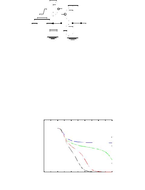
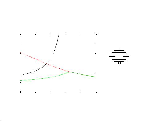
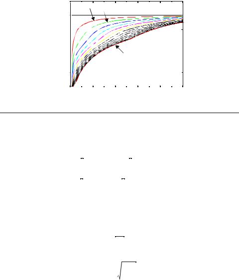
Example 6.10 Sizing of a Level Restorer
Analyzing the circuit as a whole is nontrivial, because the restoring transistor acts as a feedback device. One way to simplify the circuit for manual analysis is to open the feedback loop and to ground the gate of the restoring transistor when determining the switching point (this is a reasonable assumption, as the feedback only becomes effective once the inverter starts to switch). Hence, Mr and Mn form a “pseudo-NMOS-like” configuration, with Mr the load transistor and Mn acting as a pull-down device to GND. Assume that the inverter M1, M2 is sized to have the switching point at VDD/2 (NMOS: 0.5μm/0.25μm and PMOS: 1.5μm/0.25μm). Therefore, node X must be pulled below VDD/2 in order to switch the inverter and shut off Mr.
This is confirmed in Figure 6.38, which shows the transient response as the size of the level restorer is varied while keeping the size of Mn fixed (0.5μm/0.25μm). As the simulation indicates, for sizes above 1.5μm/0.25μm, node X can’t be brought below the switching threshold of the inverter and can’t switch the output. The detailed derivation of sizing requirement will be presented in the sequential design chapter. An important point to observe here is that the sizing of Mr is critical for DC functionality, not just performance!
Voltage, V
3.0 
2.0 
1.0 
0.00
|
W/Lr =1.75/0.25 |
|
|
||
|
|
|
W/Lr =1.50/0.25 |
|
|
W/Lr =1.0/0.25 |
W/Lr =1.25/0.25 |
|
|||
100 |
200 |
300 |
400 |
|
|
500 |
|||||
|
|
Time, ps |
|
|
|
Figure 6.37Transient response of the circuit in Figure 6.36. A level restorer that is too large can result in incorrect evaluation.
Another concern is the influence of the level restorer on the switching speed of the device. Adding the restoring device increases the capacitance at the internal node X, slowing down the gate. The rise time of the gate is further negatively affected, since, the levelrestoring transistor Mr fights the decrease in voltage at node X before being switched off.
230 |
DESIGNING COMBINATIONAL LOGIC GATES IN CMOS |
Chapter 6 |
On the other hand, the level restorer reduces the fall time, since the PMOS transistor, once turned on, speeds the pull-up action.
Problem 6.5 Device Sizing in Pass Transistors
For the circuit shown in Figure 6.36, assume that the pull-down device consists of 6 pass transistors in series each with a device size of 0.5μm/0.25μm (replacing transistor Mn). Determine the maximum W/L size for the level restorer transistor for correct functionality.
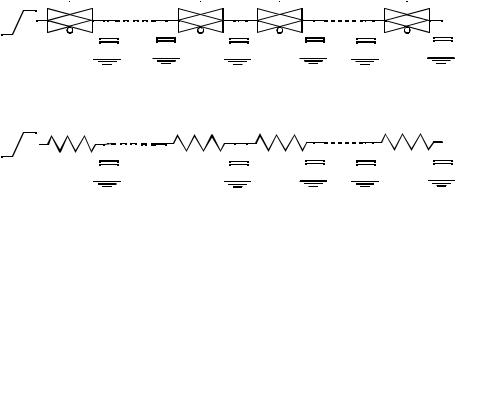
A modification of the level restorer to differential pass transistors is shown in Figure 6.38, know as swing restored pass transistor logic. Instead of a simple inverter or half latch at the output of the pass transistor network, two back-to-back inverters configured in a cross coupled fashion are used for level restoration and performance improvement. Inputs are fed to both the gate and source/drain terminals as in the case of conventional pass transistor networks. Figure 6.38 shows a simple XOR/XNOR gate of three variables A, B and C. Notice that the complementary network can be optimized by sharing transistors between the true and complementary outputs.
|
|
VDD |
VDD |
|
|
|
|
|
|
VDD |
|
|
|
|
|
|
VDD |
|
|
|
|
|||||||||||||||||||
|
|
|
|
|
|
|
|
|
|
|
|
|
|
|
|
|
|
|
|
|
|
|
|
|
|
|
|
|
|
|
|
|
|
|
||||||
|
|
|
|
|
|
|
|
|
|
|
|
|
|
|
|
|
|
|
|
|
|
|
|
|
|
|
|
|
|
|
|
|
|
|
||||||
|
|
M2 |
|
|
|
|
|
|
|
|
M2 |
Out |
|
|
|
|
|
|
|
|
|
|
|
|
|
|
|
|
|
|||||||||||
Out |
|
|
|
|
|
|
|
|
|
|
|
|
|
|
|
|
|
M2 |
|
|
|
|
|
|
|
M2 |
|
Out |
||||||||||||
|
|
|
|
|
|
|
|
|
|
|
|
|
|
|
|
|
|
|
|
|
Out |
|
|
|
|
|
|
|
|
|
|
|
|
|
|
|||||
|
|
|
|
|
|
|
|
|
|
|
|
|
|
|
|
|
|
|
|
|
|
|
|
|
|
|
|
|
|
|
|
|
|
|
|
|
|
|||
|
|
M1 |
|
|
|
|
|
|
|
|
|
M1 |
|
|
|
|
|
|
|
|
|
|
|
|
|
|
|
|
|
|
|
|
|
|
||||||
|
|
|
|
|
|
|
|
|
|
|
|
|
|
|
|
|
|
|
|
|
|
|
|
|
|
M1 |
|
|
|
|
|
|
|
M1 |
|
|
|
|
||
|
|
|
|
|
|
|
|
|
|
|
|
|
|
|
|
|
|
|
|
|
|
|
|
|
|
|
|
|
|
|
|
|
|
|
|
|
||||
|
|
|
|
|
|
|
|
|
|
|
|
|
|
|
|
|
|
|
|
|
|
|
|
|
|
|
|
|
|
|
|
|
|
|
|
|
|
|
|
|
|
|
|
|
|
|
|
|
|
|
|
|
|
|
|
|
|
|
|
|
|
|
|
|
|
|
|
|
|
|
|
|
|
|
|||||||
|
|
|
|
Complementary Output |
|
|
|
|
|
|
|
|
|
|
|
|
|
|
|
|
|
|
|
|
|
|
||||||||||||||
|
|
|
|
|
|
|
|
|
|
|
|
|
|
|
|
|
|
|
|
|
|
|||||||||||||||||||
|
|
NMOS Pass Transistor Network |
|
C |
|
|
|
C |
|
|
|
|
|
|
|
|
|
|
C |
|
|
|
C |
|||||||||||||||||
|
|
|
|
|
|
|
|
|
|
|
|
|
|
|
|
|
||||||||||||||||||||||||
|
|
|
|
|
|
|
|
|
|
|
|
|
|
|
|
|
|
|
|
|
|
|
|
|
|
|
|
|
|
|
|
|
|
|
|
|||||
|
|
|
|
|
|
|
|
|
|
|
|
|
|
|
|
|
|
|
|
|
|
|
|
|
|
|
|
|
|
|
|
|
|
|
|
|
|
|
|
|
|
|
|
|
|
|
|
|
|
|
|
|
|
|
|
|
|
|
|
|
|
|
|
|
|
|
|
|
|
|
|
|
|
|
|
|
|
|
|
|
|
|
|
|
|
|
|
|
|
|
|
|
|
|
|
|
|
|
|
|
|
B |
|
|
|
B |
|
|
|
|
|
|
|
|
|
|
B |
|
|
|
B |
|
|
|
|
|
|
|
|
|
|
|
|
|
|
|
|
|
|
|
|
|
|
|
|
|
|
|
|
|
|
|
|
|
|
|
|
|
|||||
|
|
|
|
|
|
|
|
|
|
|
|
|
|
|
|
|
|
|
|
|
|
|
|
|
|
|
|
|
|
|
|
|
|
|
|
|||||
Complementary inputs |
|
|
|
|
|
|
|
|
A |
|
|
|
A |
|
|
|
|
|
A |
A |
||||||||||||||||||||
to gate and source/drain |
|
|
|
|
|
|
|
|
|
|
|
|
|
|
|
|
|
|
|
|
|
|
|
|
|
|
|
|
|
|||||||||||
|
|
|
|
|
|
|
|
|
|
|
|
|
|
|
|
|
|
|
|
|
|
|
|
|
|
|
|
|||||||||||||
terminals |
|
|
|
|
|
|
|
|
|
|
|
|
|
|
|
|
|
|
|
|
|
|
|
|
|
|
|
|
|
|||||||||||
|
|
|
|
(a) general concept |
|
|
|
|
|
|
|
|
|
|
(b) XOR/XNOR gate |
|||||||||||||||||||||||||
Figure 6.38 Swing restored pass transistor logic [Parameswar94].
Solution 2: Multiple Threshold Transistors
A technology solution to the voltage drop problem associated with pass transistor logic is the use of multiple threshold devices. Pass transistors only pass VDD-VTn, degrading the high voltage level. One solution is to use zero threshold devices for the NMOS pass transistors, enabling passing signal close to VDD. Notice that even if the devices threshold was implanted to be exactly equal to zero, the body effect of the device prevents a swing to VDD. All devices other than the pass transistors (i.e., the inverters) are implemented using standard high threshold devices. The use of multiple threshold transistors is becoming more common and involves simple modifications to existing process flows.
Section 6.2 |
Static CMOS Design |
|
|
|
|
|
231 |
||||||||
|
|
|
|
|
VDD |
|
|
|
|
|
|
|
|||
|
0 V |
|
|
|
|
|
|
|
2.5 V |
VDD |
|||||
|
|
|
|
|
|
|
|
||||||||
|
|
|
|
|
|
|
|
||||||||
|
|
|
|
|
|
|
|
||||||||
|
|
|
|
|
|
|
|
Out |
|||||||
|
|
|
|
|
|
|
|
||||||||
|
|
|
|
|
|
|
|
|
|
|
|
|
|
|
|
|
|
|
|
|
|
|
|
|
|
|
|
|
|
|
|
|
|
|
|
|
|
|
|
|
|
|
|
|
|
|
|
|
|
|
|
|
VDD |
0 V |
|
|
|
||||||
|
|
|
|
|
|
|
|||||||||
|
|
|
|
|
|
||||||||||
|
|
||||||||||||||
|
|
||||||||||||||
|
|
|
|
|
|
|
|
||||||||
|
|
|
|
|
|
|
|
|
|
|
|
|
|
|
|
|
|
|
|
|
|
|
|
|
|
|
|
|
|
|
|
|
|
|
|
|
|
|
|
|
|
|
|
|
|
|
|
|
|
|
|
|
|
|
|
|
|
|
|
|
|
|
|
|
|
|
|
|
|
|
|
|
|
|
|
|
|
|
|
2.5 V
Figure 6.39 Static power consumption when using zero threshold pass-transistors.
The use of zero-threshold transistors can be dangerous due to the subthreshold currents that can flow through the pass-transistors, even if VGS is slightly below VT. This is demonstrated in Figure 6.39, which points out a potential sneak dc-current path. While these leakage paths are not critical when the device is switching constantly, they do pose a significant energy overhead when the device is in the idle state.
Solution 3: Transmission Gate Logic
The most widely used solution to deal with the voltage drops induced by pass transistors is the use of transmission gates. The primary limitation of NMOS or PMOS only pass gate is the threshold drop (NMOS pass device pass a strong 0 while passing a weak 1 and PMOS pass devices pass a strong 1 while passing a weak 0). The ideal approach is to use the NMOS device to pull-down and the PMOS device to pull-up. The transmission gate combines the best of both device flavors by placing a NMOS device in parallel with a PMOS device (Figure 6.40a). The control signals to the transmission gate (C and C)
|
C |
|
|
||
A |
|
|
B |
C |
|
|
|
||||
|
|
|
|
||
|
|
|
|
||
|
|
|
|
||
|
|
|
|
||
|
|
|
A |
|
B |
|
|
|
|||
C
C
(b) Symbolic representation
(a) Circuit
Figure 6.40 CMOS transmission gate.
are complementary. The transmission gate acts as a bidirectional switch controlled by the gate signal C. When C = 1, both MOSFETs are on, allowing the signal to pass through the gate. In short,
A = B if C = 1 |
(6.21) |
232 |
DESIGNING COMBINATIONAL LOGIC GATES IN CMOS |
Chapter 6 |
On the other hand, C = 0 places both transistors in cutoff, creating an open circuit between nodes A and B. Figure 6.40b shows a commonly used transmission-gate symbol.
Consider the case of charging node B to VDD for the transmission gate circuit in Figure 6.41a. Node A is driven to VDD and transmission gate is enabled (C = 1 and C= 0). If only the NMOS pass device were present, node B will charge up to VDD-VTn at which point the NMOS device turns off. However, since the PMOS device is present and turned on (
VGSp = -VDD), node B charge all the way up to VDD. Figure 6.41b shows the case for discharging node B to 0. B is initially at VDD and node A is driven low. The PMOS pass tran-
sistor by itself can only pull-down node B to VTp at which point the PMOS device turns off. the parallel NMOS device however is turned on (since its VGS = VDD) and pulls down node B all the way to GND. Though the transmission gate requires two transistors and more control signals, it enables rail-to-rail swing.
|
C = VDD |
|
C = VDD |
||||||
A = VDD |
|
|
B (initially at 0) |
A = 0 |
|
|
B (initially at VDD) |
||
|
|
|
|
||||||
|
|
|
|
||||||
|
|
|
|
|
|
||||
|
|
|
|
|
|
|
|
||
|
|
|
|
|
|
|
|
||
|
|
|
|
|
|
|
|
|
|
|
|
|
|
|
|
|
|
|
|
|
|
|
|
|
|
|
|
|
|
|
|
|
|
|
|
|
|
|
|
|
C = 0 |
|
C = 0 |
||||||
|
|
|
|
|
|
||||
(a) charing node B |
(a) discharing node B |
||||||||
Figure 6.41Transmission gates enable rail-to-rail switching
Transmission gates can be used to build some complex gates very efficiently. Figure 6.42 shows an example of a simple inverting two-input multiplexer. This gate either selects input A or B based on the value of the control signal S, which is equivalent to implementing the following Boolean function:
F = (A × S + B × S) |
(6.22) |
A complementary implementation of the gate requires eight transistors instead of six. Another example of the effective use of transmission gates is the popular XOR cir-
cuit shown in Figure 6.43. The complete implementation of this gate requires only six transistors (including the inverter used for the generation of B), compared to the twelve transistors required for a complementary implementation. To understand the operation of this circuit, we have to analyze the B = 0 and B = 1 cases separately. For B = 1, transistors M1 and M2 act as an inverter while the transmission gate M3/M4 is off; hence F = AB. In the opposite case, M1 and M2 are disabled, and the transmission gate is operational, or F = AB. The combination of both results in the XOR function. Notice that, regardless of the values of A and B, node F always has a connection to either VDD or GND and is hence a low-impedance node. When designing static-pass transistor networks, it is essential to adhere to the low-impedance rule under all circumstances. Other examples where trans- mission-gate logic is effectively used are fast adder circuits and registers.
Section 6.2 |
Static CMOS Design |
|
|
|
|
|
|
233 |
||||||||||||
|
|
|
|
|
|
|
|
|
|
|
|
|
|
|
|
|
|
S |
S |
|
|
|
|
|
|
|
|
|
|
|
|
|
|
|
|
VDD |
|
|
|
|
|
|
S |
|
|
|
|
VDD |
|
|
|
|
|
|
|
|
||||||
A |
|
|
|
|
|
|
|
|
|
|
|
|
|
|
|
|
|
|
|
|
|
|
|
|
|
|
|
|
|
|
|
|
|
|
|
|
|
|
|
|
|
|
|
|
|
|
|
|
|
|
|
M2 |
|
|
|
|
|
|
|
Out |
||
|
|
|
|
|
|
|
|
|
|
|
|
|
|
|
|
|
||||
S |
|
|
|
|
|
|
|
|
|
|
|
F |
|
|
|
|
|
|
|
|
|
|
|
|
|
|
|
|
|
|
|
|
|
|
|
|
|
|
|||
|
|
|
|
|
|
|
|
|
|
|
|
|
|
|
|
|
|
|
||
|
|
|
|
|
|
|
|
|
|
|
M1 |
|
|
|
|
|
|
|
|
|
|
|
|
|
|
|
|
|
|
|
|
|
|
|
|
|
|
|
|
||
B |
|
|
|
|
|
|
|
|
|
|
|
|
|
|
|
|
|
|
|
|
|
|
|
|
|
|
|
|
|
|
|
|
|
|
|
|
|
|
|
|
|
|
|
|
|
|
|
|
|
|
|
|
|
|
|
|
|
|
|
|
||
|
|
|
|
|
|
|
|
|
|
|
|
|
|
|
|
|
|
|
|
|
|
S |
|
|
|
|
|
|
|
|
|
|
|
|
|
|
|||||
|
|
|
|
|
|
|
|
|
|
|
|
|
|
GND |
|
|
|
|
||
|
|
|
|
|
|
|
|
|
|
|
|
|
|
|
|
|
|
S |
S |
|
|
|
|
|
|
|
|
|
|
|
|
|
|
|
|
|
|
|
|
||
|
|
|
|
|
|
|
|
|
|
|
|
|
|
|
|
|
|
|
|
|
|
|
|
|
|
|
|
|
|
|
|
|
|
|
|
|
|
A |
|
B |
|
|
|
|
|
|
|
|
|
|
|
Figure 6.42 Transmission gate multiplexer and its layout. |
||||||||||
|
|
|
|
|
|
|
|
|
|
B |
|
|
|
|
|
|
|
|
||
|
|
|
|
|
|
|
|
|
|
|
|
|
B |
|
|
|
|
|||
|
|
|
|
|
|
|
|
|
|
|
|
|
|
|
|
|
||||
|
|
|
|
|
|
|
|
|
|
|
|
|
|
|
|
|
||||
|
|
|
|
|
|
|
|
M2 |
|
|
|
|
||||||||
A |
|
|
|
|
|
|
|
|
|
|
A |
|
|
|
|
|||||
|
|
|
|
|
|
|
|
|
|
|
|
|
|
|||||||
|
|
|
|
|
|
|
|
|
|
|
F |
|
|
|
|
|
|
|
||
|
|
|
|
|
|
|
|
|
|
|
|
|
|
|
|
|
|
|||
|
|
|
|
|
|
|
|
|
|
|
|
|
|
|
|
|
|
|||
|
|
|
|
|
|
|
|
|
M1 |
|
|
M3/M4 |
Figure 6.43 Transmission gate XOR. |
|||||||
|
|
|
|
|
|
|
|
|
|
|
||||||||||
|
|
|
|
|
|
|
|
|
||||||||||||
|
|
|
|
|
|
|
|
|
|
|
||||||||||
|
|
|
|
|
|
|
|
|
|
|
|
|
B |
|
|
|
|
|||
|
|
|
|
|
|
|
|
|
|
|
|
|
|
|
|
|
|
|
|
|
|
|
|
|
|
|
|
|
|
|
B |
|
|
|
|
|
|
|
|
||
Resistance and Delay of Transmission Gate Logic
The transmission gate is, unfortunately, not an ideal switch, and has a series resistance associated with it. To quantify the resistance, consider the circuit in Figure 6.44, which involves charging a node from 0 V to VDD. In this discussion, we will us the large signal definition of resistance which involves dividing the voltage across the switch by the drain current. The effective resistance of the switch is modeled as a parallel connection of
the resistances Rn and Rp of the NMOS and PMOS devices, defined as (VDD – Vout)/In and (VDD – Vout)/Ip, respectively. The currents through the devices are obviously dependent on
the value of Vout and the operating mode of the transistors. During the low-to-high transition, the pass-transistors traverse through a number of operation modes. Figure 6.44 shows the individual resistances and the combined parallel resistance. For low values of Vout, the the NMOS device is saturated and the resistance is approximated as:
234 |
|
DESIGNING COMBINATIONAL LOGIC GATES IN CMOS |
Chapter 6 |
||||||||||||||
Rn = |
VDD – Vout |
= |
|
|
|
|
VDD – Vout |
|
|
|
|
|
|||||
-------------I-- |
N--------------- |
----æ---W-----ö------- |
æ--- |
------ |
----------- |
-------- |
---------- |
--------- |
------- |
------ |
------------------ |
---- |
-------2-------------- |
|
|
||
|
|
k¢ |
(V |
|
– V |
|
– V |
|
)V |
|
– |
VDSATö |
|
||||
|
|
|
---- |
ç |
DD |
out |
Tn |
DSAT |
---------2---------- |
÷ |
|
||||||
|
|
|
|
n è L øN è |
|
|
|
|
|
ø |
|
||||||
|
|
|
|
|
VD D – Vout |
|
|
|
|
|
|
|
|
||||
|
|
|
» k---n----(--V----D----------D -–----V----o----u---t----–----V----T---n----)---V---D-----S----A-----T |
|
|
|
|
(6.23) |
|||||||||
The resistance goes up for increasing values of Vout, and approaches infinity when Vout reaches VDD-VTn, this is when the device shuts off. Similarly, we can analyze the behavior of the PMOS transistor. When Vout is small, the PMOS is saturated, but it enters the linear mode of operation for Vout approaching VDD. The resistance then approximated by:
VDD – Vout R = ------------------------------
p IP
= |
|
|
|
VDD – Vout |
|
|
||
--- |
------------------------------------ |
|
------------ |
|
------------------------------- |
(---V----out---------–----------------------VDD)2ö-- |
||
kp × |
æ |
(–VDD – VTp)(Vout – VDD) – |
||||||
è |
----------------2----------------- |
ø |
||||||
|
|
1 |
|
|
|
|
|
|
|
|
» k---p----(--V----D-----D-----–------ |
|
V----T----p----- |
|
) |
|
(6.24) |
|
|
|
|
|
||||
The simulated value of Req = Rp || Rn as a function of Vout is plotted in Figure 6.44. It can be observed that Req is relatively constant (» 8kW in this particular case). The same is
true in other design instances (for instance, when discharging CL). When analyzing trans- mission-gate networks, the simplifying assumption that the switch has a constant resistive value is therefore acceptable.
|
30 |
|
|
|
|
2.5 V |
|
|
|
|
|
Rn |
|
Rn |
|||
|
|
|
|
|||||
|
|
|
|
|
||||
ohms |
20 |
|
Rp |
|
|
|
||
|
|
|
||||||
|
|
2.5 V |
|
|
Vout |
|||
|
|
|
|
|||||
Resistance, |
|
|
|
|
||||
|
|
|
|
|
|
|||
|
|
|
|
|
||||
|
|
|
|
|
||||
|
|
Rn || Rp |
|
|
|
|
Rp |
|
|
|
|
|
|
|
|
|
|
|
10 |
|
|
|
|
0 V |
|
|
|
|
|
|
|
|
|
|
|
|
0 |
|
1.0 |
2.0 |
|
|
|
|
|
|
|
|
|
|
|||
|
0.0 |
|
|
|
|
|||
Vout, V
Figure 6.44 Simulated equivalent resistance of transmission gate for low-to-high transition
(for (W/L)n = (W/L)p = 0.5mm/0.25mm). A similar response for overall resistance is obtained for the high-to-low transition
Problem 6.6 Equivalent Resistance During Discharge
Determine the equivalent resistance by simulation for the high-to-low transition of a transmission gate (this is, produce a plot similar to the one presented in Figure 6.44).
Section 6.2 Static CMOS Design |
235 |
An important consideration is the delay associated with a chain of transmission gates. Figure 6.45 shows a chain of n transmission gates. Such a configuration often occurs in circuits such as adders or deep multiplexors. Assume that all transmission gates are turned on and a step is applied at the input. To analyze the propagation delay of this network, the transmission gates are replaced by their equivalent resistances Req. This produces the network of Figure 6.45b.
2.5 |
|
|
|
2.5 |
|
|
2.5 |
|
|
|
2.5 |
|
||||
|
|
V1 |
Vi-1 |
|
|
Vi |
|
|
Vi+1 |
Vn–1 |
|
|
Vn |
|||
|
|
|
|
|
|
|
|
|||||||||
In |
|
|
|
|
|
|
||||||||||
|
|
|
|
C |
|
|
|
C |
|
|
C |
|
C |
|
|
C |
0 |
|
|
0 |
|
0 |
|
0 |
|||||||||
|
|
|
|
|
|
|
|
|
||||||||
|
|
|
|
(a) A chain of transmission gates |
|
|
|
|
|
|
||||||
|
Req |
V1 |
|
Req |
Vi |
Req |
Vi+1 |
Vn-1 |
Req |
Vn |
||||||
In |
|
|
|
|
|
|
|
|||||||||
|
|
|
|
C |
|
|
|
C |
|
|
C |
|
C |
|
|
C |
|
|
|
|
|
|
|
|
|
|
|
|
|||||
|
|
|
|
|
|
|
|
|
|
|
|
|||||
|
|
|
|
|
|
|
|
|
|
|
|
|
|
|
|
|
(b) Equivalent RC network
Figure 6.45 Speed optimization in transmission-gate networks.
The exact analysis of delay is not simple, but as disussed earlier, we can estimate the dominant time constant at the output of a chain of n transmission gates as follows:
|
|
|
n |
|
|
|
|
|
|
n(n + 1) |
|
τ(V |
|
) = |
å |
CR |
|
k = |
CR |
|
(6.25) |
||
n |
eq |
eq |
------------------- |
||||||||
|
|
|
|
|
2 |
|
|||||
|
|
|
k = |
0 |
|
|
|
|
|
|
|
This means that the propagation delay is proportional to n2 and increases rapidly with the number of switches in the chain.
Example 6.11 Delay through 16 transmission gates
Consider 16 minimimum sized transmission gates with an average resistance of 8 kΩ. The node capacitance consists of the capacitance of two NMOS devices (junction and gate) and the capacitance two PMOS devices (junctions and gate). Since the gate inputs are assumed to be fixed, there is no miller multiplication. The capacitance can be calculated to be approximately 3.6fF for the low-to-high transition. The delay is given by:
t |
p |
= 0.69 × CR |
n----(---n----+-----1----) |
= 0.69 × (3.6 fF)(8K W)æ |
16-------(---16------- |
+-----1----)ö |
» 2.7ns |
(6.26) |
|
|
eq 2 |
è |
2 |
ø |
|
|
The transient response for this particular example is shown in Figure 6.46. The simulated delay is 2.7ns. It is remarkable that a simple RC model predicts the delay accu-
236 |
DESIGNING COMBINATIONAL LOGIC GATES IN CMOS |
Chapter 6 |
rately. It is also clear that the use of long pass transistor chains causes significant delay degradation.
Voltage, V
3.0 
Out1 Out2
2.0 
Out16
1.0 
0.00 |
2 |
4 |
6 |
8 |
10 |
|
|
Time (ns) |
|
|
|
Figure 6.46Transient response of 16 transmission gates cascaded in series.
The most common approach for delaing with the long delay is to break the chain every m switches and to insert buffers (Figure 6.46). Assuming a propagation delay tbuf for each buffer, the overall propagation delay of the transmission-gate/buffer network can be computed as follows,
t |
|
= 0.69 |
|
n |
|
|
m(m + 1) |
|
+ |
æ n |
|
ö |
t |
|
||||
|
|
|
|
|
|
|
||||||||||||
|
|
---CR |
|
---------------------- |
|
|
|
|
|
--- – 1 |
|
|||||||
|
p |
|
|
m |
|
eq |
2 |
|
|
|
|
|
èm |
|
ø |
|
buf |
|
|
|
= 0.69 |
|
CR |
n(m + 1) |
|
+ |
|
æ n |
|
ö |
t |
|
|
(6.27) |
|||
|
|
|
|
|
|
|
|
|
||||||||||
|
|
|
--------------------- |
|
|
|
|
--- – 1 |
|
|
|
|||||||
|
|
|
|
|
eq |
|
2 |
|
|
|
|
èm |
ø |
|
buf |
|
||
The resulting delay exhibits only a linear dependence on the number of switches n, in contrast to the unbuffered circuit, which is quadratic in n. The optimal number of switches mopt between buffers can be found by setting the derivative
¶tp ¶m
to 0, which yields
mopt |
tpbuf |
(6.28) |
= 1.7 ----------- |
||
|
CReq |
|