

DEEP SUBMICRON CMOS DESIGN |
Appendix A – Design Rules |
Design
A Rules
This section gives information about the design rules used by Microwind2. You will find all the design rule values common to all CMOS processes. All that rules, as well as process parameters and analog simulation parameters are detailed here.
1. Lambda Units
The Microwind software works is based on a lambda grid, not on a micro grid. Consequently, the same layout may be simulated in any CMOS technology. The value of lambda is half the minimum polysilicon gate length. Table A-xxx gives the correspondence between lambda and micron for all CMOS technologies available in the companion CD-ROM.
Technology file available in the CD-Rom |
Minimum gate |
Value of lambda |
|
length |
|
Cmos12.rul |
1.2µm |
0.6µm |
Cmos08.rul |
0.7µm |
0.35µm |
Cmos06.rul |
0.5µm |
0.25µm |
Cmos035.rul |
0.4µm |
0.2µm |
Cmos025.rul |
0.25µm |
0.125µm |
Cmos018.rul |
0.2µm |
0.1µm |
Cmos012.rul |
0.12µm |
0.06µm |
Cmos90n.rul |
0.1µm |
0.05µm |
Cmos70n.rul |
0.07µm |
0.035µm |
Cmos50n.rul |
0.05µm |
0.025µm |
Table 1-xxx: correspondence between technology and the value of lambda in µm
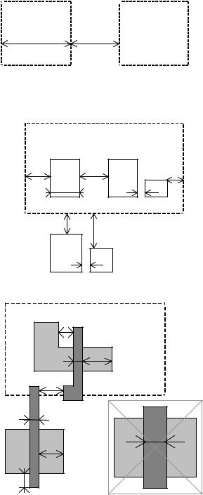
2. Layout Design Rules
The software can handle various technologies. The process parameters are stored in files with the appendix '.RUL'. The default technology corresponds to a generic 6-metal 0.12µm CMOS process. The default file is CMOS012.RUL. To select a new foundry, click on File -> Select Foundry and choose the appropriate technology in the list.
A-1 |
E. Sicard, S. Delmas-Bendhia |
20/12/03 |
DEEP SUBMICRON CMOS DESIGN |
Appendix A – Design Rules |
N-Well |
|
|
|
|
|
|
|
r101 |
Minimum well size |
12 λ |
|
|
|
|
|
r102 |
Between wells |
12 λ |
|
|
R101 |
|
|
r110 |
Minimum well area |
144 λ2 |
|
R101 |
|
|
|
|
|
|
nwell |
|
|
|
|
Diffusion |
|
|
|
|
Nwell |
|
|
r201 |
Minimum N+ and P+ diffusion width |
4 λ |
|
|
|
||
r202 |
Between two P+ and N+ diffusions |
4 λ |
|
polarization |
|
||
|
|
|
|
||||
r203 |
Extra nwell after P+ diffusion : |
6 λ |
|
|
|
|
|
r204: |
Between N+ diffusion and nwell |
6 λ |
r203 |
|
|
r205 |
|
r205 |
Border of well after N+ polarization |
2 λ |
P+ diff |
r202 |
P+ diff |
|
|
r206 |
Between N+ and P+ polarization |
0 λ |
|
|
|
N+ |
|
r207 |
Border of Nwell for P+ polarization |
|
|
|
|||
6 λ |
|
|
|
|
|||
r210 |
Minimum diffusion area |
|
r201 |
|
r206 |
|
|
|
24 λ2 |
|
nwell |
||||
|
|
|
|||||
|
|
|
|
r204 |
|
r207 |
|
|
|
|
|
|
|
||
|
|
|
|
N+ diff |
P+ |
|
P+ polarization |
|
|
|
|
|
|
||
|
|
|
|
r206 |
|
|
|
Polysilicon |
|
|
|
|
|
|
|
r301 |
Polysilicon width |
2λ |
|
r305 |
|
|
|
R302 |
Polysilicon gate on |
2 λ |
|
|
|
|
|
|
|
|
|
|
|||
|
diffusion |
|
|
|
|
|
|
R303 |
Polysilicon gate on |
4 λ |
|
P+diff |
|
|
|
|
diffusion for high |
|
|
|
|
|
|
|
voltage MOS |
|
|
r302 |
r306 |
|
|
R304 |
Between two |
3 λ |
|
|
|
|
|
|
|
|
|
|
|||
|
polysilicon boxes |
|
|
|
|
|
|
R305 |
Polysilicon vs. other |
2 λ |
r301 |
r304 |
|
|
|
|
diffusion |
|
|
|
|
||
|
|
|
|
|
|
||
R306 |
Diffusion after |
4 λ |
|
|
|
|
r303 |
|
polysilicon |
|
|
|
|
|
|
R307 |
Extra gate after |
3 λ |
|
r306 |
|
|
|
|
polysilicon |
|
N+diff |
|
|
|
|
|
8 λ2 |
|
|
|
|
||
r310 |
Minimum surface |
|
|
|
|
||
|
|
|
|
|
|||
|
|
|
r307 |
|
|
|
|
|
|
|
|
|
|
High voltage MOS |
|
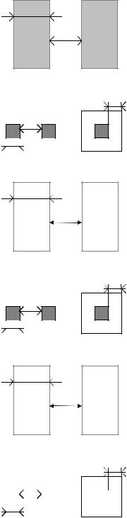
2nd Polysilicon Design Rules
A-2 |
E. Sicard, S. Delmas-Bendhia |
20/12/03 |

DEEP SUBMICRON CMOS DESIGN |
|
|
|
|
|
|
|
Appendix A – Design Rules |
||||
r311 |
Polysilicon2 width |
2 λ |
|
r311 |
|
|
|
|
Poly2 |
|||
|
|
|
|
|
||||||||
|
|
|
|
|
|
|||||||
r312 |
Polysilicon2 gate on |
2 λ |
|
|
|
|
|
|
|
|
|
|
|
|
|
|
|
|
|
|
|
|
|||
|
diffusion |
|
|
|
|
|
|
|
|
|
|
|
r320 |
Polysilicon2 |
8 λ2 |
|
|
|
|
|
|
|
|
|
|
|
minimum surface |
|
|
|
|
|
r312 |
|
||||
|
|
|
|
|
|
|||||||
MOS option |
|
|
|
|
|
|||||||
|
|
|
|
|
||||||||
|
|
|
|
|
|
|
|
|
|
|
||
|
|
|
|
|
|
|
|
|
|
|
||
|
|
|
|
|
|
|
|
|
|
|
||
rOpt |
Border of “option” layer over diff |
7λ |
|
|
|
|
|
|
|
|
||
|
N+ and diff P+ |
|
|
|
|
|
|
|
|
|
|
rOp |
|
|
|
|
N+dif |
|
|
|
|
||||
|
|
|
|
|
|
|
|
|
||||
|
|
|
|
|
|
|
|
|||||
|
|
|
|
|
|
|
|
|
|
|
|
|
|
|
|
|
|
|
|
|
|
|
|
|
|
Contact |
|
|
r401 |
Contact width |
2 λ |
r402 |
Between two contacts |
5 λ |
r403 |
Extra diffusion over contact |
2 λ |
r404 |
Extra poly over contact |
2 λ |
r405 |
Extra metal over contact |
2 λ |
r406 |
Distance between contact |
3 λ |
|
and poly gate |
|
r407 |
Extra poly2 over contact |
2 λ |
r404
r402
|
|
|
|
|
|
polysilicium |
|
|
|
|
|
||
|
r401 |
contact |
||||
r405
contact |
|
r403 |
|
r406 |
diffusion |
|
|
gate |
metal |
|
Metal 1
r501 |
Metal width |
4 λ |
|
r501 |
|
|
|
|
|
|
|
||||
r502 |
Between two metals |
4 λ |
metal |
r502 |
metal |
||
r510 |
Minimum surface |
16 λ2 |
|
|
|
|
|
|
|
|
|
|
|
|
|
Via |
|
|
r601 |
Via width |
2 λ |
r602 |
Between two Via |
5 λ |
r603 |
Between Via and |
0 λ |
|
contact |
|
r604 |
Extra metal over via |
2 λ |
r605 |
Extra metal2 over via: |
2 λ |
|
|
|
|
|
|
r604 |
|
|
|
r602 |
|
|
|
|
|
||
|
|
|
|
|
|
|||
|
|
|
|
|
|
|||
|
|
|
via |
|
|
|
|
Stacked via over |
|
|
|
|
|
|
|
||
|
|
|
|
|
|
|
||
|
|
|
metal2 |
|
||||
|
|
|
|
contact |
||||
r601 |
|
|||||||
|
|
|
|
when r603 is 0 |
||||
|
|
|
|
|||||
|
|
r603 |
|
|
|
|
|
|
contact
A-3 |
E. Sicard, S. Delmas-Bendhia |
20/12/03 |
DEEP SUBMICRON CMOS DESIGN
Metal 2 |
|
|
r701 |
Metal width:: |
4 λ |
r702 |
Between two metal2 |
4 λ |
r710 |
Minimum surface |
16 λ2 |
Via 2 |
|
|
r801 |
Via2 width : 2 λ |
|
r802 |
Between two Via2: 5 λ |
|
r804 |
Extra metal2 over via2: 2 λ |
|
r805 |
Extra metal3 over via2: 2 λ |
|
Metal 3 |
|
r901 |
Metal3 width: 4 λ |
r902 |
Between two metal3 : 4 λ |
r910 |
Minimum surface : 32 λ2 |
Via 3 |
|
ra01 |
Via3 width : 2 λ |
ra02 |
Between two Via3: 5 λ |
ra04 |
Extra metal3 over via3: 2 λ |
ra05 |
Extra metal4 over via3: 2 λ |
Metal 4 |
|
rb01 |
Metal4 width: 4 λ |
rb02 |
Between two metal4 : 4 λ |
rb10 |
Minimum surface : 32 λ2 |
Via 4 |
|
rc01 |
Via4 width : 2 λ |
rc02 |
Between two Via4: 5 λ |
rc04 |
Extra metal4 over via2: 3 λ |
rc05 |
Extra metal5 over via2: 3 λ |
Metal 5
Appendix A – Design Rules
r701
metal2 r702 metal2
r804
r802


 via2 Metal3 r801
r901
metal3 r902 metal3
ra04
ra02


 via3 Metal3,4 ra01
rb01
Metal4 rb02 Metal4
rc04
rc02
|
|
|
Via |
|
|
|
|
|
|
|
|
|
|
|
|
Metal4,5 |
||||
4 |
||||||
rc01
A-4 |
E. Sicard, S. Delmas-Bendhia |
20/12/03 |
DEEP SUBMICRON CMOS DESIGN |
Appendix A – Design Rules |
rd01 |
Metal5 width: 8 λ |
rd02 |
Between two metal5 : 8 λ |
rd10 |
Minimum surface : 100 λ2 |
rd01 |
|
|
Metal5 |
rd02 |
Metal5 |
Via 5
re01 |
Via5 width : 4 λ |
|
|
|
|
|
|
|
|
|
re04 |
|
|
|||
re02 |
Between two Via5: 6 λ |
|
|
|
|
|
|
|
|
|
|
|
|
|
|
|
|
|
|
|
|
|
|
|
|
|
|
|
|
|
|
||
re04 |
Extra metal5 over via5: 3 λ |
|
|
|
re02 |
|
|
|
|
|
|
|
|
|
||
|
|
|
|
|
|
|
|
|
|
|
|
|||||
re05 |
Extra metal6 over via5: 3 λ |
|
|
|
|
|
|
|
|
|
|
|
|
|||
|
|
|
|
|
|
|
|
|
|
|
|
|
|
|
||
|
|
|
|
|
|
|
|
|
|
|
|
|
|
|
|
|
|
|
|
|
|
|
|
|
Via5 |
|
Metal5,6 |
||||||
|
|
|
|
|
|
|
|
|
|
|
|
|
|
|
||
|
|
re01 |
|
|
|
|
|
|
|
|||||||
Metal 6
rf01 |
Metal6 width: 8 λ |
rf02 |
Between two metal6 : 15 λ |
rf10 |
Minimum surface : 300 λ2 |
rf01 |
|
|
Metal6 |
rf02 |
Metal6 |
3. Pads
The rules are presented below in µm. In .RUL files, the rules are given in lambda. As the pad size has an almost constant value in µm, each technology gives its own value in λ.
rp01 |
Pad width: |
100 µm |
rp02 |
Between two pads |
100 µm |
rp03 |
Opening in passivation v.s via : |
5µm |
rp04 |
Opening in passivation v.s metals: |
5µm |
rp05 |
Between pad and unrelated active |
20 µm |
|
area : |
|
rp03 |
PAD |
rp02 |
rp01 |
4. Electrical Extraction Principles
MICROWIND2 includes a built-in extractor from layout to electrical circuit. Worth of interest are the
MOS devices, capacitance and resistance. The flow is described in figure A-xxx.
A-5 |
E. Sicard, S. Delmas-Bendhia |
20/12/03 |
DEEP SUBMICRON CMOS DESIGN |
|
|
|
|
|
|
|
Appendix A – Design Rules |
||||||||||
|
|
|
|
|
|
|
|
|
|
|
|
|
|
|
|
|
||
|
|
|
|
|
|
|
|
|
|
|
|
|
|
|
|
|
|
|
|
Layout |
|
|
|
|
|
|
|
|
|
|
|
|
|
|
|||
|
|
|
|
|
|
|
|
|
|
|
|
|
|
|
||||
|
|
|
|
|
|
|
|
|
|
|
|
|
|
|||||
|
|
|
|
|
|
|
|
|
|
|
|
|
|
|
|
|
|
|
|
|
|
|
|
|
|
|
|
|
|
|
|
|
|
|
|
|
|
|
|
|
|
|
|
|
|
|
|
Skip in case of big circuits |
|
|||||||
|
|
|
|
|
|
|
|
|
|
|
||||||||
|
Clean layout |
|
|
|
|
|
|
|
||||||||||
|
|
|
|
|
|
|
|
|
|
|
|
|
|
|
|
|||
|
|
|
|
|
|
|
|
|
|
- |
|
Extract MOS width |
||||||
|
|
|
|
|
|
|
|
|
|
|
||||||||
|
|
|
|
|
|
|
|
|
|
|||||||||
|
Extract devices |
|
|
|
|
|
|
|
- |
|
Extract MOS length |
|||||||
|
|
|
|
|
|
|
- |
|
Extract MOS option |
|||||||||
|
|
|
|
|
|
|
|
|
|
|
||||||||
|
|
|
|
|
|
|
|
|
|
|
|
|
|
|
- Extract all electrical nets |
|||
|
|
|
|
|
|
|
|
|
|
|
|
|
|
|
||||
|
Extract interconnects |
|
|
|
|
|
|
|
||||||||||
|
|
|
|
|
|
|
- |
Extract net capacitance |
||||||||||
|
|
|
|
|
|
|
|
|
|
|||||||||
- Extract coupling capacitance between nets - Extract net resistance
Create SPICE netlist
Figure A-xxx: Extraction of the electrical circuit from layout
The first step consists in cleaning the layout. Mainly, redundant boxes are removed, overlapping boxes are transformed into non-overlapping boxes. In the case of complex circuits, MICROWIND2 may skip this cleaning step as it required a significant amount of computational time.
5. Node Capacitance extraction
Each deposited layer is separated from the substrate by a SiO2 oxide and generated by a parasitic capacitor. The unit is the aF/µm2 (atto = 10-18 ). Basically all layers generate parasitic capacitors. Diffused layers generate junction capacitors (N+/P-, P+/N). The list of capacitance handled by MICROWIND2 is given below. The name corresponds to the code name used in CMOS012.RUL (CMOS 0.12µm). Surface capacitance refers to the body. Vertical crosstalk capacitance refer to interlayer coupling capacitance, while lateral crosstalk capacitance refer to adjacent interconnects.
|
|
|
|
|
|
|
|
|
|
|
|
|
|
|
Inter-layer |
|
|
|
|
|
|
|
|
||||
|
|
|
|
|
|
|
|
|
|
|
|
|
|
|
|
|
|
|
|
|
|
|
|||||
|
|
|
|
|
|
|
|
|
|
|
|
|
|
|
|
|
|
|
|
|
|
|
|
|
|
|
|
|
|
|
|
|
|
|
|
|
To body |
|
|
|
|
|
Adjacent layers |
|
|
||||||||||
|
|
Frindging |
|
|
|
|
|
|
|
|
|
|
|
|
|
|
|||||||||||
|
|
capacitance |
|
|
|
|
|
|
|
|
|
|
|
|
|
|
|
|
|
|
|
||||||
|
|
|
|
|
|
|
|
|
|
|
|
|
|
|
|
|
|
|
|
|
|||||||
|
|
|
|
|
|
|
|
|
|
|
|
|
|
|
|
|
|
|
|
|
|
|
|
|
|
|
|
|
|
|
|
|
|
|
|
|
|
|
|
|
|
|
|
|
|
|
|
|
|
|
|
|
|
|
|
|
|
|
|
|
|
|
|
|
|
|
|
Surface |
|
|
|
|
|
|
|
|
|||||||
|
|
|
|
|
|
|
|
|
|
|
|
|
|
|
|
|
|
|
|
||||||||
|
|
|
|
|
|
|
|
|
|
|
|
capacitance |
|
|
|
|
|
|
|
|
|||||||
|
|
|
|
|
|
|
|
|
|
|
|
|
|
|
SUBSTRATE BODY |
|
|
|
|
|
|
|
|
||||
|
|
|
|
|
|
|
|
|
|
|
|
|
|
|
|
|
|
|
|
|
|
|
|
|
|
|
|
|
|
|
|
|
|
|
|
|
|
|
|
Figure A-1: Capacitances |
|
|
|||||||||||||
SURFACE CAPACITANCE |
|
|
|
|
|
|
|
|
|||||||||||||||||||
|
|
|
|
|
|
|
|
|
|||||||||||||||||||
|
NAME |
|
|
|
DESCRIPTION |
|
LINEIC |
SURFACE |
|||||||||||||||||||
|
|
|
|
|
|
|
|
|
|
|
|
|
|
|
|
|
|
|
|
|
(aF/µm) |
(aF/µm2) |
|||||
|
CpoOxyde |
|
|
|
Polysilicon/Thin oxide capacitance |
|
n.c |
4600 |
|||||||||||||||||||
A-6 |
E. Sicard, S. Delmas-Bendhia |
20/12/03 |
DEEP SUBMICRON CMOS DESIGN |
|
Appendix A – Design Rules |
|||
|
|
|
|
|
|
|
CpoBody |
Polysilicon to substrate capacitance |
n.c |
|
80 |
|
CMEBody |
Metal on thick oxide to substrate |
42 |
|
28 |
|
CM2Body |
Metal2 on body |
36 |
|
13 |
|
CM3Body |
Metal3 on body |
33 |
|
10 |
|
CM4Body |
Metal4 on body |
30 |
|
6 |
|
CM5Body |
Metal5 on body |
30 |
|
5 |
|
CM6Body |
Metal6 on body |
30 |
|
4 |
INTER-LAYER CROSSTALK CAPACITANCE |
|
||
|
NAME |
DESCRIPTION |
VALUE (aF/µm2) |
|
CM2Me |
Metal2 on metal 1 |
50 |
|
CM3M2 |
Metal3 on metal 2 |
50 |
|
CM4M3 |
Metal4 on metal 3 |
50 |
|
CM5M4 |
Metal5 on metal 4 |
50 |
|
CM6M5 |
Metal6 on metal 5 |
50 |
LATERAL CROSSTALK CAPACITANCE |
|
||
|
|
|
|
|
NAME |
DESCRIPTION |
VALUE (aF/µm) |
|
CMeMe |
Metal to metal (at 4λ distance, 4λ width) |
10 |
|
CM2M2 |
Metal2 to metal 2 |
10 |
|
CM3M3 |
Metal3 to metal 3 |
10 |
|
CM4M4 |
Metal4 to metal 4 |
10 |
|
CM5M5 |
Metal5 to metal 5 |
10 |
|
CM6M6 |
Metal6 to metal6 |
10 |
CM3M3
Metal 3
CM2M2
Metal 2
CMeMe
Metal 1
|
w= 4λ |
d= 4λ |
|
|
|
|
|
|
|
SUBSTRATE BODY |
|
|
|
|
|
Figure A-2: Crosstalk capacitance
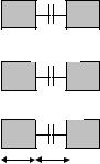
The crosstalk capacitance value per unit length is given in the design rule file for a predefined interconnect width (w=4λ) and spacing (d=4λ).
In Microwind2, the computed crosstalk capacitance is not dependant on the interconnect width w.
The computed crosstalk capacitance value is proportional to 1/d where d is the distance between interconnects.
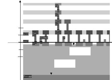
Parameters for Vertical Aspect of the Technology
The vertical aspect of the layers for a given technology is described in the RUL file after the design rules,
using code HE (height) and TH (thickness) for all layers. The figure A-3 below illustrates the altitude 0,
which corresponds to the channel of the MOS. The height of diffused layers can be negative, for P++ EPI
layer for example.
A-7 |
E. Sicard, S. Delmas-Bendhia |
20/12/03 |
DEEP SUBMICRON CMOS DESIGN |
Appendix A – Design Rules |
Layer altitude (in µm)
2.0
1.0
Altitude 0.0
-1.0
-2.0
STI height is negative
EPI height is negative
Figure A-2: Description of the 2D aspect of the CMOS technology
LAYER |
DESCRIPTION |
PARAMETERS |
EPI |
Buried layer made of P++ used to create a |
HEEPI for height (negative in |
|
good ground reference underneath the active |
respect to the origin) |
|
area. |
THEPI for thickness |
STI |
Shallow trench isolation used to separate the |
HESTI for height |
|
active areas. |
THSTI for thickness |
PASSIVATION |
Upper SiO2 oxide on the top of the last metal |
HEPASS for height |
|
layer |
THPASS for thickness |
NITRIDE |
Final oxide on the top of the passivation, |
HENIT for height |
|
usually Si3N4. |
THNIT for thickness |
NISO |
Buried N- layer to isolate the Pwell |
HENBURRIED for height |
|
underneath the nMOS devices, to enable |
THNBURRIED for thickness |
|
forward bias and back bias |
|
6. Resistance Extraction
NAME |
DESCRIPTION |
VALUE (Ω) |
RePo |
Resistance per square for polysilicon |
4 |
RePu |
Resistance per square for unsalicide polysilicon |
40 |
ReP2 |
Resistance per square for polysilicon2 |
4 |
ReDn |
Resistance per square for n-diffusion |
100 |
ReDp |
Resistance per square for p-diffusion |
100 |
ReMe |
Resistance per square for metal |
0.05 |
ReM2 |
Resistance per square for metal 2 (up to 6) |
0.05 |
ReCo |
Resistance for one contact |
20 |
ReVi |
Resistance for one via (up to via5) |
2 |
Dielectrics
Some options are built in Microwind to enable specific features of ultra deep submicron technology. Details are provided in the table below.
A-8 |
E. Sicard, S. Delmas-Bendhia |
20/12/03 |

DEEP SUBMICRON CMOS DESIGN |
Appendix A – Design Rules |
||||||||||||||
|
|
|
|
|
|
|
|
|
|
|
|
|
|
|
|
|
CODE |
|
DESCRIPTION |
|
EXAMPLE VALUE |
||||||||||
|
HIGHK |
|
Oxide for interconnects (SiO2) |
|
4.1 |
|
|
||||||||
|
|
|
|
|
|
|
|
|
|
|
|
||||
|
GATEK |
|
Gate oxide |
|
4.1 |
|
|
||||||||
|
|
|
|
|
|
|
|
|
|
|
|
||||
|
LOWK |
|
Inter-metal oxide |
|
3.0 |
|
|
|
|
||||||
|
LK11 |
|
Inter-metal1 oxide |
|
3.0 |
|
|
||||||||
|
|
|
|
|
|
|
|
|
|
|
|
||||
|
LK22 |
|
Inter-metal2 oxide (up to LK66) |
|
3.0 |
|
|
||||||||
|
|
|
|
|
|
|
|
|
|
|
|
||||
|
LK21 |
|
Metal2-Metal1 oxide |
|
3.0 |
|
|
||||||||
|
|
|
|
|
|
|
|
|
|
|
|
||||
|
LK32 |
|
Metal3-Metal2 oxide (up to LK65) |
|
3.0 |
|
|
||||||||
|
|
|
|
|
|
|
|
|
|
|
|
||||
|
TOX |
|
Normal MOS gate oxide thickness |
|
0.004 µm (40 Å) |
||||||||||
|
HVTOX |
|
High voltage gate oxide thickness |
|
|
|
0.007 µm (70 Å) |
||||||||
|
|
|
|
|
|
|
|
|
|
|
|
||||
|
Substrate |
|
|
|
|
|
|
|
|
|
|
|
|
|
|
|
LOWK |
|
|
|
|
|
|
LK44 |
|
|
|
|
|
||
|
Metal 4 |
|
|
|
|
|
Metal 4 |
|
|
|
|||||
|
|
|
|
|
|
|
|
|
|
|
|
|
|||
|
|
HIGHK |
|
|
|
|
|
|
LK43 |
|
|||||
|
|
|
|
|
|
|
|
|
|
|
|
|
|
|
|
|
Metal 3 |
LOWK |
|
|
|
|
|
Metal 3 |
LK33 |
|
|
|
|
|
|
|
|
|
|
|
|
|
|
|
|
|
|
|
|
|
|
|
|
HIGHK |
|
|
|
|
|
|
LK32 |
|
|||||
|
Metal 2 |
|
|
|
|
|
|
Metal 2 |
|
|
|
|
|
|
|
|
LOWK |
|
|
|
|
|
LK22 |
|
|
|
|
|
|||
|
|
|
|
|
|
|
|
|
|
|
|||||
|
|
|
|
|
|
|
|
|
|
|
|
|
|||
|
|
HIGHK |
|
|
|
|
|
|
LK21 |
|
|||||
|
Metal 1 |
|
|
|
|
|
|
Metal 1 |
|
|
|
|
|
|
|
|
LOWK |
|
|
|
|
|
LK11 |
|
|
|
|
|
|||
|
|
|
|
|
|
|
|
|
|
|
|
|
|||
|
|
|
|
|
|
|
|
|
|
|
|
|
|
|
|
|
|
HIGHK |
|
|
|
|
|
|
LK01 |
|
|||||
|
|
|
|
|
|
|
|
|
|
|
|
|
|
|
|
|
|
|
|
Substrate |
|
|
|
Substrate |
|
||||||
|
|
|
|
|
|
|
|
|
|
|
|
|
|
|
|
|
|
|
Using LOWK, HIGHK with |
Using Lkii, LKij with non- |
|||||||||||
|
|
|
homogeneous oxide structure |
homogeneous oxide structure |
|||||||||||
Fig. A-xxx: Illustration of the use of LOWK, HIGHK dielectric constants (left figure) or detailed permittivity for each layer (right figure)
7. Simulation Parameters
The following list of parameters is used in Microwind2 to configure the simulation.
CODE |
DESCRIPTION |
TYPICAL VALUE |
VDD |
Supply voltage of the chip |
2.0 V |
HVDD |
High voltage supply |
3.3V |
DELTAT |
Simulator minimum time step to ensure convergence. |
0.5e-12 s |
|
You may increase this value to speed up the simulation |
|
|
but instability problems may rise. |
|
TEMPERATURE |
Operating temperature of the chip |
25 °C |
Models Level1 and Level3 for analog simulation
A-9 |
E. Sicard, S. Delmas-Bendhia |
20/12/03 |
DEEP SUBMICRON CMOS DESIGN |
Appendix A – Design Rules |
Four types of MOS devices may be described as detailed in figure 12-4 (Data from SIA, 0.12µm CMOS technology). In the rule file, the keyword "MOS1", "MOS2', "MOS3" and "MOS4" are used to declare the device names appearing in menus. In 0.12µm technology, three types of MOS devices are declared as follows. Also, NMOS & PMOS keywords are used to select n-channel Mos or p-channel Mos device parameters.
Parameter |
MOS1 |
MOS2 |
MOS3 |
Default name |
High Speed |
Low Leakage |
High voltage |
Vt (nmos) |
0.3 |
0.5 |
0.7 |
Vt (pmos) |
-0.3 |
-0.5 |
-0.7 |
KP (nmos) |
300 |
300 |
200 |
KP (pmos) |
150 |
150 |
100 |
* MOS definition
*
MOS1 low leakage
MOS2 high speed
MOS3 high voltage
Figure 12-5: Description of MOS options in 0.12µm technology (cmos012.RUL)
The list of parameters for level 1 and level 3 is given below:
PARAMETER |
KEYWORD |
DEFINITION |
TYPICAL VALUE 0.25µm |
|
|
|
|
NMOS |
pMOS |
VTO |
l3vto |
Threshold voltage |
0.4V |
-0.4V |
U0 |
l3u0 |
Low field mobility |
0.06 m2/V.s |
0.025 m2/V.s |
PHI |
l3phi |
Surface potential at strong |
0.3V |
0.3V |
|
|
inversion |
|
|
LD |
l3ld |
Lateral diffusion into |
0.01µm |
0.01µm |
|
|
channel |
|
|
GAMMA |
l3gamma |
Bulk threshold parameter |
0.4 V0.5 |
0.4 V0.5 |
KAPPA |
l3kappa |
Saturation field factor |
0.01 V-1 |
0.01 V-1 |
VMAX |
l3vmax |
Maximum drift velocity |
150Km/s |
100Km/s |
THETA |
l3theta |
Mobility degradation |
0.3 V-1 |
0.3 V-1 |
|
|
factor |
|
|
NSS |
l3nss |
Sub-threshold factor |
0.07 V-1 |
0.07 V-1 |
TOX |
l3tox |
Gate oxide thickness |
3nm |
3nm |
CGSO |
L3cgs |
Gate to Source lineic |
100.0pF/m |
100.0pF/m |
|
|
capacitance |
|
|
CGDO |
L3cgd |
Gate to drain overlap |
100.0pF/m |
100.0pF/m |
|
|
capacitance |
|
|
CGBO |
L3cb |
Gate to bulk overlap |
1e-10F/m |
1e-10F/m |
|
|
capacitance |
|
|
CJSW |
L3cj |
Side-wall source & drain |
1e-10F/m |
1e-10F/m |
|
|
capacitance |
|
|
A-10 |
E. Sicard, S. Delmas-Bendhia |
20/12/03 |