

chapter7_pub.fm Page 280 Wednesday, November 22, 2000 8:41 AM
280 |
DESIGNING SEQUENTIAL LOGIC CIRCUITS |
Chapter 7 |
derive that the propagation delay of node Q is approximately equal to the delay of the pseudo-NMOS inverter formed by (M5-M6) and M2. To obtain the delay for node Q, it is sufficient to add the delay of the complementary CMOS inverter M3-M4.
Example 7.2 Propagation Delay of Static SR Flip-Flop
The transient response of the latch in Figure 7.8, as obtained from simulation, is plotted in Figure 7.10. The devices are sized as described in Example 7.1, and a load of a single inverter is assumed for each latch output. The flip-flop is initially in the reset state, and an S-pulse is applied. As we can observe, this results first in a discharging of the Q output while Q stays at 0. Once the switching threshold of the inverter M3-M4 is reached, the Q output starts to rise. The delay of this transient is solely determined by the M3-M4 inverter, which is hampered by the slow rise time at its input. From the simulation results, we can derive that tpQ and tpQ equal 120psec and 230psec, respectively.
3.0
2.0
SET |
Q |
Q |
Volts
tpQ tpQ
1.0
Figure 7.10 Transient response of SR flip-flop.
0.0 |
1.0 |
1.1 |
1.2 |
1.3 |
1.4 |
1.5 |
0.9 |
Time (ns)
Problem 7.2 Complimentary CMOS SR FF
Instead of using the modified SR FF of Figure 7.8, it is also possible to use complementary logic to implement the clocked SR FF. Derive the transistor schematic (which consists of 12 transistors). This circuit is more complex, but switches faster and consumes less switching power. Explain why.
7.4.3Multiplexer Based Latches
There are many approaches for constructing latches. One very common technique involves the use of transmission gate multiplexers. Multiplexer based latches can provide similar functionality to the SR latch, but has the important added advantage that the sizing of devices only affects performance and is not critical to the functionality.
Figure 7.11 shows an implementation of static positive and negative latches based on multiplexers. For a negative latch, when the clock signal is low, the input 0 of the mul-
chapter7_pub.fm Page 281 Wednesday, November 22, 2000 8:41 AM
Section 7.4 |
Static Latches and Registers |
281 |
tiplexer is selected, and the D input is passed to the output. When the clock signal is high, the input 1 of the multiplexer, which connects to the output of the latch, is selected. The feedback holds the output stable while the clock signal is high. Similarly in the positive latch, the D input is selected when clock is high, and the output is held (using feedback) when clock is low.
|
|
Negative Latch |
|
|
|
Positive Latch |
|
||||||||||||
|
|
|
|
|
|
|
|
|
|
|
|
|
|
|
|
|
|
|
Q |
|
|
|
|
1 |
|
|
|
Q |
|
|
|
0 |
|
|
|
||||
D |
|
|
|
0 |
|
|
|
|
D |
|
|
|
|
1 |
|
|
|
|
|
|
|
|
|
|
|
|
|
|
|
|
|
|
|
|
|||||
|
|
|
|
|
|
|
|
|
|
|
|
|
|
|
|
|
|
|
|
|
|
|
|
|
|
|
|
|
|
|
|
|
|
|
|
|
|
|
|
|
|
|
|
|
|
|
|
|
|
|
|
|
|
|
|
|
|
|
|
CLK |
CLK |
|
Figure 7.11 Negative and positive latches based on multiplexers.
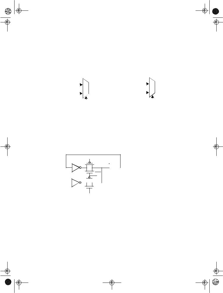
A transistor level implementation of a positive latch based on multiplexers is shown in Figure 7.12. When CLK is high, the bottom transmission gate is on and the latch is transparent - that is, the D input is copied to the Q output. During this phase, the feedback loop is open since the top transmission gate is off. Unlike the SR FF, the feedback does not have to be overridden to write the memory and hence sizing of transistors is not critical for realizing correct functionality. The number of transistors that the clock touches is important since it has an activity factor of 1. This particular latch implementation is not particularly efficient from this metric as it presents a load of 4 transistors to the CLK signal.
CLK

 Q
Q
CLK
D |
|
|
|
|
|
|
|
Figure 7.12Transistor level implementation of |
|
|
|
|
|
|
a positive latch built using transmission gates.
CLK
It is possible to reduce the clock load to two transistors by using implement multiplexers using NMOS only pass transistor as shown in Figure 7.13. The advantage of this approach is the reduced clock load of only two NMOS devices. When CLK is high, the latch samples the D input, while a low clock-signal enables the feedback-loop, and puts the latch in the hold mode. While attractive for its simplicity, the use of NMOS only pass transistors results in the passing of a degraded high voltage of VDD-VTn to the input of the first inverter. This impacts both noise margin and the switching performance, especially in the case of low values of VDD and high values of VTn. It also causes static power dissipation in first inverter, as already pointed out in Chapter 6. Since the maximum input-voltage to the inverter equals VDD-VTn, the PMOS device of the inverter is never turned off, resulting is a static current flow.
chapter7_pub.fm Page 282 Wednesday, November 22, 2000 8:41 AM
282 |
|
|
|
|
|
|
|
|
|
|
|
|
|
|
DESIGNING SEQUENTIAL LOGIC CIRCUITS |
Chapter 7 |
|||||||||||||||
|
|
|
|
|
|
|
|
|
|
|
|
|
|
|
|
|
|
|
|
|
|
|
|
|
|
|
|
|
|
|
|
|
|
CLK |
|
|
|
|
|
|
|
|
|
|
|
|
|
|
|
|
QM |
|
CLK |
|
|
|
|
|
|||||
|
|
|
|
|
|
|
|
|
|
|
|
|
|
|
|
|
|
|
|
|
|
||||||||||
|
|
|
|
|
|
|
|
|
|
|
|
|
|
|
|
|
|
|
|
|
|
|
|
|
|||||||
D |
|
|
|
|
|
|
|
|
|
|
|
|
|
|
|
|
|
|
|
|
|
QM |
|
|
|
|
|
|
|
|
|
|
|
|
|
|
|
|
|
|
|
|
|
|
|
|
|
|
|
|
|
|
|
|
|
|
|
|
|
|
|||
|
|
|
|
|
|
|
|
|
|
|
|
|
|
|
|
|
|
|
|
|
|
|
|
|
|
|
|
||||
|
|
|
|
|
|
|
|
|
|
|
|
|
|
|
|
|
|
|
|
|
|
|
|
|
|
|
|||||
|
|
|
|
|
|
|
|
|
|
|
|
|
|
|
|
|
|
|
|
|
|
|
|
|
|
|
|
|
|
|
|
|
|
|
|
|
|
|
|
|
|
|
|
|
|
|
|
|
|
|
|
|
|
|
|
|
|
|
|
|
|
||
|
|
|
|
|
|
|
|
|
|
|
|
|
|
|
|
|
|
|
|
|
|
|
|
CLK |
|
|
|
|
|
|
|
|
|
|
|
|
|
|
|
|
|
|
|
|
|
|
|
|
|
|
|
|
|
|
|
|
|
|
|
|
|
|
|
|
|
|
|
|
|
|
|
|
|
|
|
|
|
|
|
|
|
|
|
|
|
|
|
|
|
|
|
|
|||
|
|
|
|
|
|
|
|
|
|
|
|
|
|
|
|
|
|
|
|
|
|
|
|
|
|
|
|
||||
|
|
|
|
|
|
|
|
|
|
|
|
|
|
|
|
|
|
|
|
|
|
|
|
|
|||||||
|
|
|
|
|
|
|
|
|
CLK |
|
|
|
|
|
|
|
|
|
|
|
|
|
|
|
|||||||
|
|
|
|
|
|
(a) Schematic diagram |
|
|
|
|
|
|
|
|
(b) Nonoverlapping clocks |
||||||||||||||||
Figure 7.13 Multiplexer based NMOS latch using NMOS only pass transistors for multiplexers.
7.4.4Master-Slave Based Edge Triggered Register
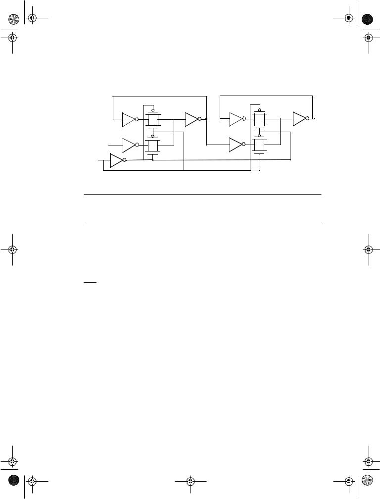
The most common approach for constructing an edge-triggered register is to use a master-slave configuration as shown in Figure 7.14. The register consists of cascading a negative latch (master stage) with a positive latch (slave stage). A multiplexer based latch is used in this particular implementation, though any latch can be used to realize the master and slave stages. On the low phase of the clock, the master stage is transparent and the D input is passed to the master stage output, QM. During this period, the slave stage is in the hold mode, keeping its previous value using feedback. On the rising edge of the clock, the master slave stops sampling the input, and the slave stage starts sampling. During the high phase of the clock, the slave stage samples the output of the master stage (QM), while the master stage remains in a hold mode. Since QM is constant during the high phase of the clock, the output Q makes only one transition per cycle. The value of Q is the value of D right before the rising edge of the clock, achieving the positive edge-triggered effect. A negative edge-triggered register can be constructed using the same principle by simply switching the order of the positive and negative latch (i.e., placing the positive latch first).
|
|
|
|
|
|
|
|
|
|
|
|
|
|
Slave |
|
|
|||
|
|
|
|
|
Master |
|
|
|
|
|
|
|
|
|
|
CLK |
|||
|
|
|
|
|
|
|
|
|
|
|
|
|
|
||||||
|
|
|
|
|
|
|
|
|
|
|
|
|
|
|
|
|
|
|
D |
|
|
|
|
|
|
|
|
|
|
|
|
|
|
|
|
|
|
||
|
|
|
|
|
|
|
|
|
|
|
|
0 |
|
|
|
|
Q |
||
|
|
|
|
1 |
|
|
|
|
|
|
|
1 |
|
|
|
|
QM |
||
|
|
|
|
|
|
|
|
|
|
|
|
|
|
|
|||||
|
|
|
|
|
|
|
|
|
|
|
|
|
|
|
|
|
|
||
D |
|
|
|
|
0 |
|
|
|
QM |
|
|
|
|
|
|
|
|
Q |
|
|
|
|
|
|
|
|
|
|
|
|
|
|
|
|
|
|
|
|
|
CLK
CLK
Figure 7.14 Positive edge-triggered register based on a master-slave configuration.
A complete transistor level implementation of a the master-slave positive edge-trig- gered register is shown in Figure 7.15. The multiplexer is implemented using transmission gates as discussed in the previous section. When clock is low (CLK = 1), T1 is on and T2 is off, and the D input is sampled onto node QM. During this period, T3 is off and T4 is on and the cross-coupled inverters (I5, I6) holds the state of the slave latch. When the clock goes high, the master stage stops sampling the input and goes into a hold mode. T1 is off and T2
chapter7_pub.fm Page 283 Wednesday, November 22, 2000 8:41 AM
Section 7.4 |
Static Latches and Registers |
283 |
is on, and the cross coupled inverters I3 and I4 holds the state of QM. Also, T3 is on and T4 is off, and QM is copied to the output Q.
I2 |
T2 |
I3 |
I5 |
T4 |
I6 |
Q |
D |
|
|
QM |
|
|
|
|
|
I4 |
T3 |
|
|
|
I1 |
T1 |
|
|
|
||
CLK |
|
|
|
|
|
|
Figure 7.15 |
Transistor-level implementation of a master-slave postive edge-triggered |
|
||||
register using multiplexers.
Problem 7.3Optimization of the Master Slave Register
It is possible to remove the inverters I1 and I2 from Figure 7.3 without loss of functionality. Is there any advantage in including these inverters in the implementation?
Timing Properties of the multiplexer Bases Master-Slave Register. As discussed earlier, there are three important timing metrics in registers: the set up time, the hold time and the propagation delay. It is important to understand these factors that affect the timing parameters and develop the intuition to manually estimate the parameters. Assume that the propagation delay of each inverter is tpd_inv and the propagation delay of the transmission gate is tpd_tx. Also assume that the contamination delay is 0 and the inverter delay to derive
CLK from CLK has a delay equal to 0.
The set-up time is the time before the rising edge of the clock that the input data D must become valid. Another way to ask the question is how long before the rising edge does the D input have to be stable such that QM samples the value reliably. For the transmission gate multiplexer-based register, the input D has to propagate through I1, T1, I3 and I2 before the rising edge of the clock. This is to ensure that the node voltages on both terminals of the transmission gate T2 are at the same value. Otherwise, it is possible for the cross-coupled pair I2 and I3 to settle to an incorrect value. The set-up time is therefore
equal to 3 *tpd_inv + tpd_tx .
The propagation delay is the time for the value of QM to propagate to the output Q. Note that since we included the delay of I2 in the set-up time, the output of I4 is valid before the rising edge of clock. Therefore the delay tc-q is simply the delay through T3 and
I6 (tc-q = tpd_tx + tpd_inv).
The hold time represents the time that the input must be held stable after the rising edge of the clock. In this case, the transmission gate T1 turns off when clock goes high and therefore any changes in the D-input after clock going high are not seen by the input. Therefore, the hold time is 0.
chapter7_pub.fm Page 284 Wednesday, November 22, 2000 8:41 AM
284 |
DESIGNING SEQUENTIAL LOGIC CIRCUITS |
Chapter 7 |
Example 7.3 Timing analysis using SPICE.
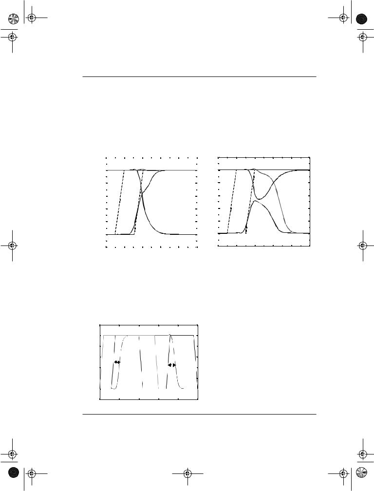
To obtain the set-up time of the register using SPICE, we progressively skew the input with respect to the clock edge until the circuit fails. Figure 7.16 shows the set-up time simulation assuming a skew of 210 psec and 200 psec. For the 210 psec case, the correct value of input D is sampled (in this case, the Q output remains at the value of VDD). For a skew of 200 psec, an incorrect value propagates to the output (in this case, the Q output transitions to 0). Node QM starts to go high while the output of I2 (the input to transmission gate T2) starts to fall. However, the clock is enabled before the two nodes across the transmission gate (T2) settle to the same value and therefore, results in an incorrect value written into the master latch.The set-up time for this register is therefore 210 psec.
|
3.0 |
|
|
|
|
|
|
|
|
|
|
3.0 |
|
|
|
|
|
|
|
|
|
|
|
Q |
|
|
|
|
|
|
|
|
|
|
|||
|
2.5 |
|
|
|
|
|
|
|
|
2.5 |
|
|
|
|
|
|
||
|
|
|
|
|
|
|
|
|
|
|
|
|
|
|
|
|
||
|
2.0 |
|
|
|
|
|
QM |
|
|
|
|
2.0 |
|
|
|
|
|
|
|
1.5 |
|
|
|
|
|
|
|
|
|
Volts |
1.5 |
|
|
|
|
I2-T2 |
|
Volts |
|
|
CLK |
|
|
|
|
|
|
D |
CLK |
|
|
|||||
|
|
D |
|
|
|
|
|
|
|
|
|
|||||||
|
|
|
|
|
|
|
|
|
|
|
|
|
||||||
|
|
|
|
|
|
|
|
|
|
|
1.0 |
|
|
|
|
|
|
|
|
1.0 |
|
|
|
|
|
|
|
|
|
|
|
|
|
|
QM |
|
|
|
|
|
|
|
|
|
I2-T2 |
|
|
|
|
|
|
|
|
|
|
|
|
0.5 |
|
|
|
|
|
|
|
|
|
0.5 |
|
|
|
|
|
|
|
|
|
|
|
|
|
|
|
|
|
|
|
|
|
|
|
|
||
|
0.0 |
|
|
|
|
|
|
|
|
|
|
0.0 |
|
|
|
|
|
|
|
|
|
|
|
|
|
|
|
|
|
|
|
|
|
|
|||
|
-0.5 |
|
|
|
|
|
|
|
|
|
-0.5 |
|
|
|
|
|
|
|
|
|
|
|
|
|
|
|
|
0 |
0.2 |
|
0.4 |
0.6 |
|||||
|
|
|
0.2 |
0.4 |
0.6 |
0.8 |
1 |
|
||||||||||
|
0 |
|
|
|
|
|||||||||||||
|
|
|
|
|
|
time(ns) |
|
|
|
|
|
|
|
|
|
time (ns) |
||
|
|
|
|
(a) T |
setup |
= 0.21ns |
|
|
|
|
|
|
|
(b) Tsetup = 0.20ns |
||||
Figure 7.16 Set-up time simulation.
Q
0.81
In a similar fashion, the hold time can be simulated. The D input edge is once again skewed relative to the clock signal till the circuit stop functioning. For this design, the hold time is 0 - i.e., the inputs can be changed on the clock edge. Finally, for the propagation delay, the inputs are transitioned at least a set-up time before the rising edge of the clock and the delay is measured from the 50% point of the CLK edge to the 50% point of the Q output. From this simulation (Figure 7.17), tc-q (lh) was 160psec and tc-q(hl) was 180psec.
Volts
2.5 
CLK
1.5 
D
tc-q(lh) |
|
|
Figure 7.17 Simulation of propagation delay. |
Q |
tc-q(hl) |
||
|
|
|
|
0.5 
-0.5 0 |
0.5 |
1 |
1.5 |
2 |
2.5 |
time, ns
chapter7_pub.fm Page 285 Wednesday, November 22, 2000 8:41 AM
Section 7.4 |
Static Latches and Registers |
285 |
As mentioned earlier, the drawback of the transmission gate register is the high capacitive load presented to the clock signal. The clock load per register is important since it directly impacts the power dissipation of the clock network. Ignoring the overhead required to invert the clock signal (since the buffer inverter overhead can be amortized over multiple register bits), each register has a clock load of 8 transistors. One approach to reduce the clock load at the cost of robustness is to make the circuit ratioed. Figure 7.18 shows that the feedback transmission gate can be eliminated by directly cross coupling the inverters.
|
|
CLK |
|
|
|
|
|
|
|
CLK |
|
|
|
|
|
|
|
|
|
|
|||||||
D |
|
|
|
|
|
|
|
|
|
I1 |
|
|
|
|
|
|
|
|
|
|
|
|
|
|
|
|
|
|
|
|
|
|
|
|
|
|
|
|
|
|
|
|
|
|
|
|
|
|
|
|
|
|
|||
|
|
T1 |
|
|
|
|
|
|
|
|
T2 |
|
|
|
I3 |
|
|
|
Q |
||||||||
|
|
|
|
|
|
|
|
|
|
|
|
|
|
|
|
||||||||||||
|
|
|
|
|
|
|
|
|
|
I2 |
|
|
|
|
|
|
|
|
|
|
I4 |
|
|
|
|
|
|
|
|
|
|
|
|
|
|
|
|
|
|
|
|
|
|
|
|
|
|
|
|
|
|
|
|
||
|
|
|
|
|
|
|
|
|
|
|
|
|
CLK |
|
|
|
|
||||||||||
|
|
CLK |
|
|
|
|
|
|
|
|
|
|
|
||||||||||||||
|
|
|
|
|
|
|
|
|
|
|
|
|
|
|
|
|
|
|
|||||||||
|
|
|
|
|
|
|
|
|
|
|
|
|
|
|
|
|
|
|
|
|
|
|
|
|
|
|
|
Figure 7.18 Reduced load clock load static master-slave register.
The penalty for the reduced clock load is increased design complexity. The transmission gate (T1) and its source driver must overpower the feedback inverter (I2) to switch the state of the cross-coupled inverter.The sizing requirements for the transmission gates can be derived using a similar analysis as performed for the SR flip-flop. The input to the inverter I1 must be brought below its switching threshold in order to make a transition. If minimum-sized devices are to be used in the transmission gates, it is essential that the transistors of inverter I2 should be made even weaker. This can be accomplished by making their channel-lengths larger than minimum. Using minimum or close-to-minimum- size devices in the transmission gates is desirable to reduce the power dissipation in the latches and the clock distribution network.
Another problem with this scheme is the reverse conduction — this is, the second stage can affect the state of the first latch. When the slave stage is on (Figure 7.19), it is possible for the combination of T2 and I4 to influence the data stored in I1-I2 latch. As long as I4 is a weak device, this is fortunately not a major problem.
|
|
|
VDD |
|
|
|
|
|
0 |
|
|
|
|
|
|
|
|
|
|
|
|
|
|
||||||
|
|
|
|
|
|
|
|
|
I1 |
|
|
|
|
|
|
|
|
|
|
|
|
|
|
|
|
|
|
|
|
|
|
|
|
|
|
|
|
|
|
|
|
|
|
|
|
|
|
|
|
|
|
|
|
|
|
|
|
||
|
|
|
T |
|
|
|
|
|
|
|
|
T |
|
|
|
|
|
I |
|
|
|
|
|
|
Q |
||||
D |
|
|
1 |
|
|
|
|
|
|
|
|
|
2 |
|
|
|
|
|
|
|
3 |
|
|
|
|
|
|
||
|
|
|
|
|
|
|
|
|
I2 |
|
|
|
|
|
|
|
|
|
|
|
|
|
I4 |
|
|
|
|
|
|
|
|
0 |
|
|
|
|
|
|
|
|
VDD |
|
|
|
|
|
|
|
|
|
|
||||||||
|
|
|
|
|
|
|
|
|
|
|
|
|
|
|
|
|
|
|
|
|
|||||||||
|
|
|
|
|
|
|
|
|
|
|
|
|
|
|
|
|
|
|
|
|
|
|
|
||||||
Figure 7.19 Reverse conduction possible in the transmission gate.
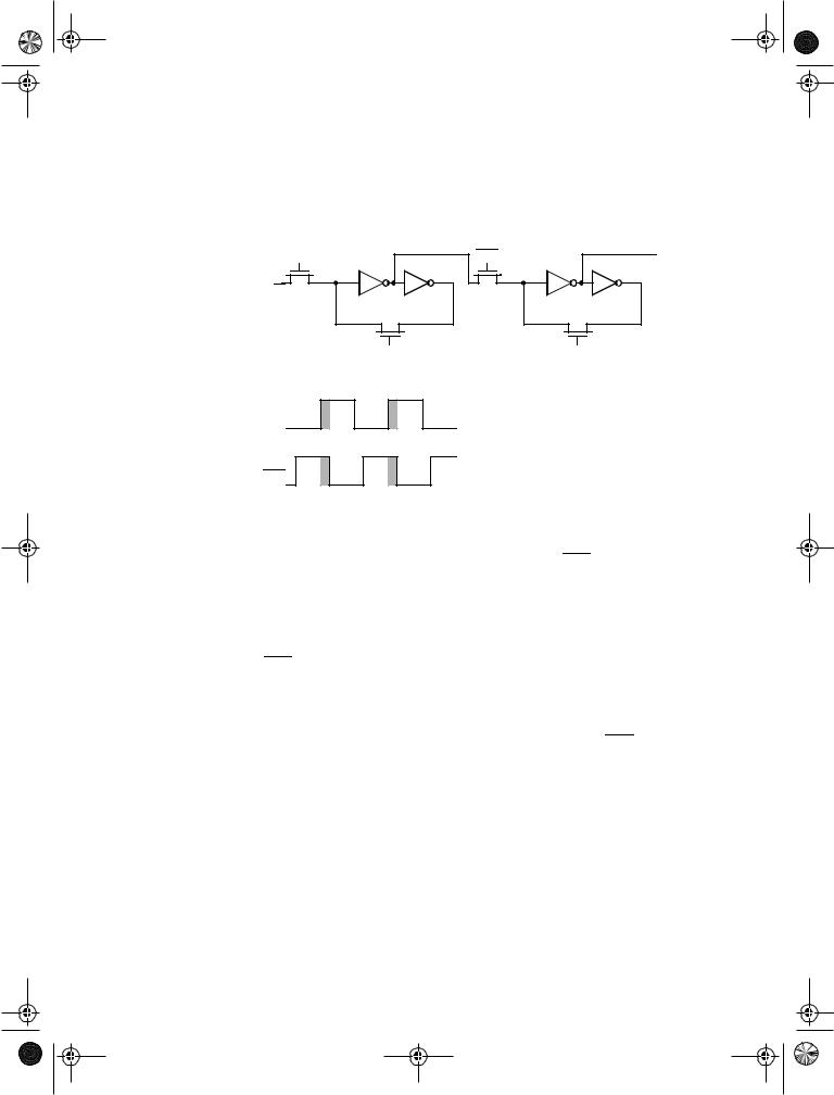
7.4.5Non-ideal clock signals
So far, we have assumed that CLK is a perfect inversion of CLK, or in other words, that the delay of the generating inverter is zero. Even if this were possible, this would still not be a good assumption. Variations can exist in the wires used to route the two clock signals, or
chapter7_pub.fm Page 286 Wednesday, November 22, 2000 8:41 AM
286 |
DESIGNING SEQUENTIAL LOGIC CIRCUITS |
Chapter 7 |
the load capacitances can vary based on data stored in the connecting latches. This effect, known as clock skew is a major problem, and causes the two clock signals to overlap as is shown in Figure 7.20b. Clock-overlap can cause two types of failures, as illustrated for the NMOS-only negative master-slave register of Figure 7.20a.
CLK |
X |
Q |
CLK |
||
D |
A |
|
B |
|
|
|
|
|
|
CLK |
|
CLK |
|||
|
|||
(a) Schematic diagram
CLK
CLK |
Figure 7.20 Master-slave register based |
|
on NMOS-only pass transistors.
(b)Overlapping clock pairs
•When the clock goes high, the slave stage should stop sampling the master stage output and go into a hold mode. However, since CLK and CLK are both high for a short period of time (the overlap period), both sampling pass transistors conduct and there is a direct path from the D input to the Q output. As a result, data at the output can change on the rising edge of the clock, which is undesired for a negative edgetriggered register. The is know as a race condition in which the value of the output Q is a function of whether the input D arrives at node X before or after the falling edge of CLK. If node X is sampled in the metastable state, the output will switch to a value determined by noise in the system.
•The primary advantage of the multiplexer-based register is that the feedback loop is open during the sampling period, and therefore sizing of devices is not critical to functionality. However, if there is clock overlap between CLK and CLK, node A can be driven by both D and B, resulting in an undefined state.
Those problems can be avoided by using two non-overlapping clocks PHI1 and PHI2
instead (Figure 7.21), and by keeping the nonoverlap time tnon_overlap between the clocks large enough such that no overlap occurs even in the presence of clock-routing delays.
During the nonoverlap time, the FF is in the high-impedance state—the feedback loop is open, the loop gain is zero, and the input is disconnected. Leakage will destroy the state if this condition holds for too long a time. Hence the name pseudostatic: the register employs a combination of static and dynamic storage approaches depending upon the state of the clock.
chapter7_pub.fm Page 287 Wednesday, November 22, 2000 8:41 AM
Section 7.4 |
Static Latches and Registers |
287 |
||||||||||||||||||||||||||||||||||
|
|
|
|
PHI1 |
|
|
|
|
|
|
|
|
PHI2 |
|
|
|
|
|
|
Q |
||||||||||||||||
|
|
|
|
|
|
|
|
|
|
|
|
|
|
|
|
|
||||||||||||||||||||
|
|
|
|
|
|
|
|
|
|
|
|
|
|
|||||||||||||||||||||||
|
D |
|
|
|
|
|
|
|
|
|
|
|
|
|
|
|
|
|
|
|
|
|
|
|
|
|
|
|
|
|
|
|
|
|
||
|
|
|
|
|
|
|
|
|
|
|
|
|
|
|
|
|
|
|
|
|
|
|
|
|
|
|
|
|
|
|
|
|
|
|
|
|
|
|
|
|
|
|
|
|
|
|
|
|
|
|
|
|
|
|
|
|
|
|
|
|
|
|
|
|
|
|
|
|
|
|
|
|
|
|
|
|
|
|
|
|
|
|
|
|
|
|
|
|
|
|
|
|
|
|
|
|
|
|
|
|
|
|
|
|
|
|
|
|
|
|
|
|
|
|
|
|
|
|
|
|
|
|
|
|
|
|
|
|
|
|
|
|
|
|
|
|
|
|
|
|
|
|
|
|
|
|
|
|
|
|
|
|
|
|
|
|
|
|
|
|
|
|
|
|
|
|
|
|
|
|
|
|
|
|
|
|
|
|
|
|
|
|
|
|
|
|
|
|
|
|
|
|
|
|
|
|
|
|
|
|
|
|
|
|
|
|
|
|
|
|
|
|
|
|
|
|
|
|
|
|
|
PHI2 |
PHI1 |
(a) Schematic diagram
PHI1
PHI2
tnon_overlap
(b) Two-phase nonoverlapping clocks
Figure 7.21 Pseudostatic two-phase D register.
Problem 7.4 Generating non-overlapping clocks
Figure 7.22 shows one possible implementation of the clock generation circuitry for generating a two-phase non-overlapping clocks. Assuming that each gate has a unit gate delay, derive the timing relationship between the input clock and the two output clocks. What is the nonoverlap period? How can this period be increased if needed?
PHI1
CLK
|
|
|
|
|
|
|
|
|
|
|
Figure 7.22Circuitry for generating a |
|
|
|
|
|
|
|
|
|
|
|
|
|
|
|
|
|
|
|
|
|
|
PHI2 |
two phase non-overlapping clock |
|
|
|
|
|
|
|
|
|
|
||
|
|
|
|
|
|
|
|
|
|
|
|
|
|
|
|
|
|
|
|
|
|
|
|
7.4.6Low-Voltage Static Latches
The scaling of supply voltages is critical for low power operation. Unfortunately, certain latch structures don’t function at reduced supply voltages. For example, without the scaling of device thresholds, NMOS only pass transistors (e.g., Figure 7.21) don’t scale well with supply voltage due to its inherent threshold drop. At very low power supply voltages, the input to the inverter cannot be raised above the switching threshold, resulting in incorrect evaluation. Even with the use of transmission gates, performance degrades significantly at reduced supply voltages.
Scaling to low supply voltages hence requires the use of reduced threshold devices. However, this has the negative effect of exponentially increasing the sub-threshold leakage power as discussed in Chapter 6. When the registers are constantly accessed, the leak-
chapter7_pub.fm Page 288 Wednesday, November 22, 2000 8:41 AM
288 |
DESIGNING SEQUENTIAL LOGIC CIRCUITS |
Chapter 7 |
age energy is typically insignificant compared to the switching power. However, with the use of conditional clocks, it is possible that registers are idle for extended periods and the leakage energy expended by registers can be quite significant.
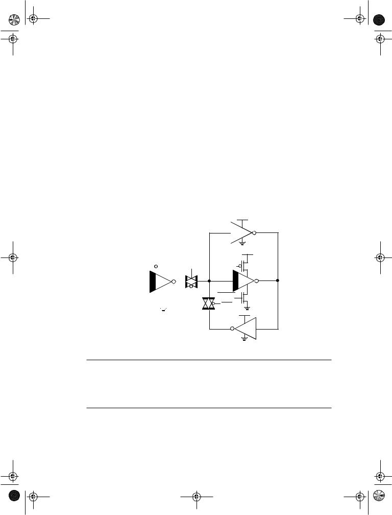
Many solutions are being explored to address the problem of high leakage during idle periods. One approach for this involves the use of Multiple Threshold devices as shown in Figure 7.23 [Mutoh95]. Only the negative latch is shown here. The shaded inverters and transmission gates are implemented in low-threshold devices. The lowthreshold inverters are gated using high threshold devices to eliminate leakage.
During normal mode of operation, the sleep devices are tuned on. When clock is low, the D input is sampled and propagates to the output. When clock is high, the latch is in the hold mode. The feedback transmission gate conducts and the cross-coupled feedback is enabled. Note there is an extra inverter, needed for storage of state when the latch is in the sleep state. During idle mode, the high threshold devices in series with the low threshold inverter are turned off (the SLEEP signal is high), eliminating leakage. It is assumed that clock is in the high state when the latch is in the sleep state. The feedback low-threshold transmission gate is turned on and the cross-coupled high-threshold devices maintains the state of the latch.
VDD
|
|
|
|
|
|
|
|
VDD |
||||||||||
|
|
|
|
|
|
|
|
|
|
|
|
|
|
|
|
|
|
|
SLEEP |
|
|
|
|
|
High VT CLK |
||||||||||||
|
|
|
|
|
||||||||||||||
|
D |
|
|
|
|
|
|
|
|
|
|
|
|
|
|
|
|
|
|
|
|
|
|
|
|
|
|
|
|
|
|
|
|||||
|
|
|
|
|
|
|
|
|
|
|
|
|||||||
|
|
|
|
|
|
|
|
|
|
High VT |
|
|
|
|||||
|
SLEEP |
|
|
|
|
|
|
|
|
|||||||||
|
|
|
|
|
|
|
|
|
|
|
|
|
CLK |
|||||
|
|
VDD |
SLEEP |
High VT |
|
|
|
|
|
|
Q |
SLEEP |
|
High VT |
CLK |
|
|
|
VDD |
|
Figure 7.23 One solution for the leakage problem in low-voltage operation using MTCMOS.
Problem 7.5Transistor minimization in the MTCMOS register
Unlike combination logic, both flavors of high threshold devices in series are required to eliminate the leakage of low threshold gates. Explain why this is the case. Hint: Eliminate the high VT NMOS or high VT PMOS of the low threshold inverter on the right of Figure 7.23 and investigate potential leakage paths.
chapter7_pub.fm Page 289 Wednesday, November 22, 2000 8:41 AM
Section 7.5 |
Dynamic Latches and Registers |
289 |
7.5Dynamic Latches and Registers
Storage in a static sequential circuit relies on the concept that a cross-coupled inverter pair produces a bistable element and can thus be used to memorize binary values. This approach has the useful property that a stored value remains valid as long as the supply voltage is applied to the circuit, hence the name static. The major disadvantage of the static gate, however, is its complexity. When registers are used in computational structures that are constantly clocked such as pipelined datapath, the requirement that the memory should hold state for extended periods of time can be significantly relaxed.
This results in a class of circuits based on temporary storage of charge on parasitic capacitors. The principle is exactly identical to the one used in dynamic logic — charge stored on a capacitor can be used to represent a logic signal. The absence of charge denotes a 0, while its presence stands for a stored 1. No capacitor is ideal, unfortunately, and some charge leakage is always present. A stored value can hence only be kept for a limited amount of time, typically in the range of milliseconds. If one wants to preserve signal integrity, a periodic refresh of its value is necessary. Hence the name dynamic storage. Reading the value of the stored signal from a capacitor without disrupting the charge requires the availability of a device with a high input impedance.
7.5.1Dynamic Transmission-Gate Based Edge-triggred Registers
A fully dynamic positive edge-triggered register based on the master-slave concept is shown in Figure 7.24. When CLK = 0, the input data is sampled on storage node 1, which has an equivalent capacitance of C1 consisting of the gate capacitance of I1, the junction capacitance of T1, and the overlap gate capacitance of T1. During this period, the slave stage is in a hold mode, with node 2 in a high-impedance (floating) state. On the rising edge of clock, the transmission gate T2 turns on, and the value sampled on node 1 right before the rising edge propagates to the output Q (note that node 1 is stable during the high phase of the clock since the first transmission gate is turned off). Node 2 now stores the inverted version of node 1. This implementation of an edge-triggered register is very efficient as it requires only 8 transistors. The sampling switches can be implemented using NMOS-only pass transistors, resulting in an even-simpler 6 transistor implementation. The reduced transistor count is attractive for high-performance and low-power systems.
CLK CLK
D |
|
|
|
|
|
|
1 |
|
|
I1 |
|
|
|
|
|
|
2 |
|
|
|
|
|
|
||||||||
|
|
|
T1 |
|
|
|
|
|
T2 |
|
|
I3 |
|
Q |
|||||||||||||||||
|
|
|
|
|
|
|
|
|
C1 |
|
|
|
|
|
|
|
|
C2 |
|
|
|
||||||||||
|
|
|
|
|
|
|
|
|
|
|
|
|
|
|
|
|
|
|
|
|
|
|
|
|
|
|
|
||||
|
|
|
|
|
|
|
|
|
|
|
|
|
|
|
|
|
|
|
|
||||||||||||
|
|
|
|
|
|
|
|
|
|
|
|
|
|
|
|
|
|
|
|
|
|
|
|
|
|
|
|
|
|
||
|
|
|
|
|
|
|
|
|
|
|
|
|
|
|
|
CLK |
|
|
|
|
|
|
|
|
|
|
|
|
|||
|
|
|
CLK |
|
|
|
|
|
|
|
|
|
|
|
|
|
|
|
Figure 7.24 |
Dynamic edge-triggered register. |
|||||||||||
|
|
|
|
|
|
|
|
|
|
|
|
|
|
|
|
|
|
|
|
|
|
|
|
|
|
||||||
The set-up time of this circuit is simply the delay of the transmission gate, and corresponds to the time it takes node 1 to sample the D input. The hold time is approximately zero, since the transmission gate is turned off on the clock edge and further inputs changes are ignored. The propagation delay (tc-q) is equal to two inverter delays plus the delay of the transmission gate T2.