

nanotechnology / nano4_10_004
.pdfINSTITUTE OF PHYSICS PUBLISHING |
NANOTECHNOLOGY |
Nanotechnology 15 (2004) S517–S524 |
PII: S0957-4484(04)75556-7 |
Transport in single-molecule transistors: Kondo physics and negative differential resistance
Lam H Yu and Douglas Natelson
Department of Physics and Astronomy, Rice University, 6100 Main Street, Houston,
TX 77005, USA
E-mail: natelson@rice.edu
Received 26 January 2004 Published 23 July 2004
Online at stacks.iop.org/Nano/15/S517 doi:10.1088/0957-4484/15/10/004
Abstract
We report two examples of transport phenomena based on sharp features in the effective density of states of molecular-scale transistors: Kondo physics in C60-based devices, and gate-modulated negative differential resistance (NDR) in ‘control’ devices that we ascribe to adsorbed contamination. We discuss the need for a statistical approach to device characterization, and the criteria that must be satisfied to infer that transport is based on single molecules. We describe apparent Kondo physics in C60-based single-molecule transistors (SMTs), including signatures of molecular vibrations in the Kondo regime. Finally, we report gate-modulated NDR in devices made without intentional molecular components, and discuss possible origins of this property.
(Some figures in this article are in colour only in the electronic version)
1. Introduction
Though active electronic devices made from molecules were originally suggested 30 years ago [1], interfacing small numbers of molecules with metal electrodes for electronic characterization has only been successful relatively recently [2, 3]. Two-terminal configurations include nanopore [4] structures [5, 6], crossed wires [7–9], mechanical break junctions [10–14], and scanned probe approaches (scanning tunnelling microscope (STM) [15–20] or conducting probe atomic force microscope (AFM) [21, 22]).
The resulting two-terminal devices exhibit a number of interesting phenomena, including molecular rectification [23], negative differential resistance (NDR) [5], and switching between low and high conductance states [7, 8, 6, 19, 20]. Several explanations for these effects have been proposed, including the electronic structure of the molecular orbitals [24, 25]; conformational changes in the molecules [26, 24, 27– 29]; vibronic-assisted inelastic tunnelling [30–32]; and dynamic switching of contact bonds [20]. A central question is whether the nonlinear effects are intrinsic to the molecules themselves, or the molecule–metal contact. Three-terminal
devices provide added tunability to test candidate explanations for nonlinear conduction in these systems.
Three-terminal nanometre-scale single-molecule transistors (SMTs) [33–39] are a rich physical system, sensitive to molecular vibrational modes [33] and exhibiting correlated many-body states (the Kondo effect) [34, 35, 38]. Such devices are tools for examining physics on the nanometre scale, and promise to be the ultimate limit of electronic device scaling.
In this paper we report two different nonlinear conductance phenomena in molecule-scale three-terminal devices. First, we show conduction in C60-based single-molecule transistors consistent with Kondo physics. The data indicate that inelastic couplings to vibrational resonances in the molecule lead to enhanced transport at finite bias in the Kondo regime. We also show that nanometre-scale metal junctions can, under certain circumstances, exhibit pronounced negative differential resistance tunable by a proximal gate electrode. We argue that this NDR most probably originates from the adsorption of a specific contaminant at the nanometre-scale interelectrode gap.
0957-4484/04/100517+08$30.00 © 2004 IOP Publishing Ltd Printed in the UK |
S517 |
L H Yu and D Natelson
(a) |
(b) |
current pulse
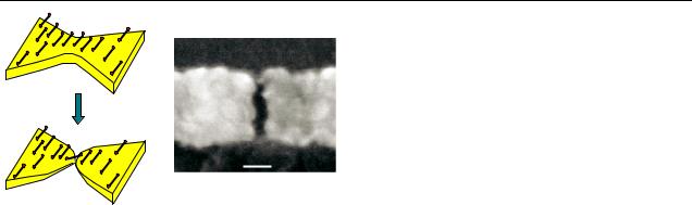
30 nm
Figure 1. (a) A diagram of the electromigration technique for the fabrication of closely spaced electrodes bridged by individual molecules. (b) A micrograph of a typical result, with electrodes separated by <3 nm.
2. Technique
Devices are prepared on an oxidized (200 nm) degenerately doped p + Si substrate that is used as an underlying gate electrode. The fabrication technique, based on controlled electromigration of lithographically fabricated metal constrictions [40], is shown in figure 1 and described in further detail in [38]. A Ti (1.5 nm)/Au (15 nm) metal constriction between two larger pads is made by electron beam lithography, e-beam evaporation, and lift-off. The surface is then exposed to oxygen plasma for 1 min to remove any organic residue from the lithography process. Batches of as many as 60 constrictions are fabricated on a single chip. The transverse dimension of the narrowest portion of the constriction is typically 80 nm.
For C60-based devices, a dilute solution (1 mg C60/4 ml toluene) of molecules is spin cast (900 rpm) onto the array of constrictions. The wafer is then placed in a variable-temperature vacuum probe station that is evacuated to10−5 mB by turbo-pump. Control devices are treated similarly, but without the fullerenes. Various common solvents have been examined, including toluene, tetrahydrofuran (THF), and methyl chloride. No particular precautions have been taken to avoid exposure to ambient atmosphere during the spinning process.
At room temperature a semiconductor parameter analyser is used to sweep an applied voltage across the junction until the junction conductance begins to degrade from electromigration. This ‘prebreaking’ is stopped once the junction resistance exceeds a few hundred ohms. Subsequent examination of such junctions by a scanning electron microscope (SEM) indicates that the junctions are nearly broken, so that the applied voltage drops almost entirely across the now nanoscale constriction.
The sample area is then cooled to 4.2 K by flowing liquid cryogens, while the chamber is isolated from the turbopumping system. By carefully heating the sample stage during this cooling process, stray gases are cryoadsorbed to the chamber walls and a carbon felt ‘sorb’ rather than onto the sample. Cryopumping creates ultrahigh vacuum (UHV) conditions at the sample while at low temperatures. Further electromigration is performed at 4.2 K, breaking the constrictions into separate source and drain electrodes while in UHV.
Figure 1(b) shows an SEM image of such an electrode pair after warming to room temperature. From all the constrictions that begin intact at room temperature, measurable conduction at a source–drain bias of 100 mV is found at the conclusion of the electromigration procedure for 70% of devices. Because metal surfaces anneal and reconstruct upon warming, it is difficult to perform precise measurements of electrode morphology. However, it appears that electrodes must be spaced by 1–3 nm for measurable conduction.
All measurements reported here were performed at dc using a semiconductor parameter analyser. For each electrode pair, one electrode (source) is defined as ground, and ID is measured as a function of VD for various values of gate voltage, VG. The differential conductance, dID/dVD, is then computed numerically. While numerical differentiation can be noisy, this procedure has the benefit of working over a very broad range of conductances.
In experiments done on the C60-decorated junctions, the devices are usually thermally cycled once over a period of two days without venting the chamber. In the NDR experiments discussed below, electrodes were thermally cycled several times over three to five days. The device characteristics measured at low temperatures varied after each thermal cycle, presumably due to electrode surface reconstruction, molecule migration, and possible adsorption of contaminants such as water.
3. Device physics
3.1. Single-electron devices
All successful nanometre-scale single-molecule transistors that have been demonstrated [33–39] act as single-electron transistors (SETs) [41]. An SET consists of an island coupled by tunnel barriers (R > RK ≡ h/e2) to source and drain electrodes, with additional capacitive coupling to a gate electrode. Accounting for electron–electron interactions on the island via a classical capacitance, one may define an electron addition energy, Ec, associated with changing the charge of the island by a single electron. For kBT Ec, it is energetically forbidden at zero source–drain bias to change the charge state of the island. The resulting suppression of transport is called Coulomb blockade. Higher order processes (e.g. cotunnelling) can allow transport in the classically blockaded regime.
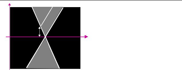
It is possible to use VG to lift the blockade at zero source– drain bias by adjusting the potential of the island so that it is energetically degenerate to change the charge of the island by one electron. Similarly, current may flow once eVD exceeds the energy addition threshold. Mapping differential conductance as a function of VD and VG, one finds a result like that shown in figure 2: diamond-shaped blockaded regions where the charge on the island is quantized, separated by a ‘crossing point’ where, at VD = 0 and with increasing VG, the occupation of the island changes from n to n + 1 electrons. The lower the capacitive coupling to the gate relative to the source and drain couplings, the more change in VG necessary to change the charge state of the island.
For a small island, Ec includes both the Coulomb repulsion, Ui , and the spacing between the ith and i + 1th
S518
Transport in single-molecule transistors
VD
∆
n |
n+1 |
VG
Figure 2. A schematic map of the differential source–drain conductance of a single-electron transistor as a function of bias and gate voltage. The brightness scale runs from zero conductance (black) to high conductance (white). The arrow indicates a resonance due to tunnelling into an excited state with energy above the lowest unoccupied island state.
single-particle electronic states, i . When inelastic processes are allowed, at sufficient bias an electron may tunnel from the source into excited single-particle states of the island, as well as the lowest available single-particle state. Transport at high bias is enhanced by these additional channels, manifested as peaks in the differential conductance that parallel the edges of the blockaded diamonds.
When the island is a nanoscale molecule, several issues arise. First, source and drain couplings are established by overlap of the molecular wavefunction with that of the conduction electrons of the leads. These couplings broaden the energies of the single-particle states by S, D, and depend crucially on the details of the metal surface, the molecular orientation, and the chemical nature of the molecular binding. Furthermore, the classical capacitance is so small that electrostatic charging energies in excess of 100 meV are reasonable. Similarly, the spacings between the single-particle molecular states can easily be hundreds of meV or more. While there is some evidence that significant renormalizations of both these quantities may occur [37], most experiments [33–36, 38] find accessing more than two charge states of a single molecule to be extremely challenging.
Because of these large level spacings, tunnelling through excited electronic states is generally not seen in SMTs. However, molecules do exhibit vibrational excitations at the meV scale. Observations of tunnelling through such excited states have been reported [33–36, 38], as have vibrational effects in other gated molecular devices [42].
A single-electron device with an unpaired spin may demonstrate nontrivial transport physics [43, 44] due to the Kondo effect [45], the formation of a many-body state comprising the unpaired spin and an antiferromagnetically coupled screening cloud of conduction electrons in the leads. The energy scale, kBTK, for the Kondo effect depends exponentially on the total coupling = S + D. It is possible to have a high Kondo temperature while still having a low total conductance, since the conductance is limited by the smaller of D, S while TK is set by their total.
The signature of a Kondo resonance in a single-electron device is the appearance of a peak in the differential conductance near zero source–drain bias when the number of charges on the island changes from even to odd. In a well-coupled system for T TK the peak conductance on resonance is expected to saturate to 2e2/ h. This value may be significantly reduced if the source and drain couplings are very asymmetric. For T TK, the peak conductance is expected to decrease logarithmically with temperature. The shape of this resonance (ID as a function of VD) may deviate from a pure Lorentzian due to Fano-type competition between Kondo resonant transport and other channels [46– 48]. In an external magnetic field, B, large enough to Zeeman split the localized unpaired spin, the Kondo peak is expected to split by an amount gµB B, where µB is the Bohr magneton and g is the Lande´ factor. Kondo physics has been reported in molecular devices incorporating metal ions [34, 35]. Our observation of C60-based devices is described below. We discuss vibrational resonances in the Kondo regime, a phenomenon only observable in molecular devices.
3.2. Negative differential resistance
Negative differential resistance is well known and understood in two-terminal devices such as p–n junctions [49], quantum well resonant tunnelling diodes [50], and scanning tunnelling spectroscopy (STS) measurements [51]. The basic mechanism for each involves energy-specific conduction of charge carriers; as the source–drain bias is swept into and out of the relevant energy range, the current varies nonmonotonically, leading to NDR over some range of bias voltage. In Esaki diodes the current peaks due to the alignment of the valence and conduction bands across the p–n junction over a limited range of bias. In quantum well devices the increase in conduction occurs when the energy of the injected carriers is resonant with a quasi-bound state of the well. Here we will explore the origin of NDR in the STS measurements [52] in more detail because we believe a similar mechanism is responsible for our NDR observations.
Consider a tunnelling spectroscopy measurement with electrons flowing from a probe tip to a conducting substrate, with a molecule attached to the substrate. To explain the observation of NDR one must abandon the common notion of a featureless tip density of states, and describe the current through the STS system with the general expression
I = |
µP |
T (E, V ) dE, |
(1) |
µS |
where µS and µP are the electrochemical potential of the metallic substrate and probe tip, respectively, with µS = µP + eV . Here T (E, V ) is the tunnelling transmission of the system. Using the transfer Hamiltonian formalism, one can relate T (E, V ) to the product of the local densities of states (LDOS) ρmol(E) and ρtip(E) of the molecule and the tip. The current through the STS system is proportional to the convolution of ρmol and ρtip within the energy range defined by µS and µP.
Suppose both the ρmol and the ρtip contain sharp peaks (such as those caused by localized surface states, for
S519
L H Yu and D Natelson
At Equilibrium
|
(a) |
|
S |
|
|
|
|
||
|
|
|
|
|
P |
|
|||
|
Energy |
|
|
|
|
|
|
|
|
|
|
|
|
|
|
|
|
||
|
|
|
|
LDOS |
|
|
|
||
S |
|
(b) |
|
(c) |
|
|
P |
||
|
|
|
|
|
|
||||
|
|
|
|
P |
|
S |
|
|
|
|
|
|
|
|
|
|
|
|
|
|
|
|
|
|
|
|
|
|
|
(d) |
S |
P |
(e) |
P |
|
|
|
|
S |
|
|
|
|
|
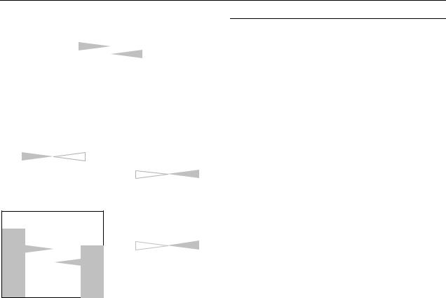
Figure 3. The energetics of substrate/molecule and tip apex/probe in STS measurements on molecules, after [52]. Sharp features represent local densities of states of the molecule (left) and the tip apex (right). Weak coupling allows a potential difference to develop between the molecule and substrate under bias. (a) At equilibrium, with substrate chemical potential, µS, and probe chemical potential, µP; (b) a positive bias V is applied to the probe, and weak apex–probe coupling is assumed, leading to the apex potential
VApex < V . The LDOS of the apex atom moves up relative to µP under bias, and NDR results; (c) a negative bias is applied to the
probe, again with |VApex | < |V |. The LDOS of the apex atom move down relative to µP, and NDR results; (d) a positive bias is applied
to the probe, with strong apex–probe coupling that forces
VApex = V . No NDR results because of the relative positions of molecule and apex LDOS; (e) a negative bias is applied to the probe,
with VApex = V . Since the LDOS of the molecule must move down with respect to the µP under bias, NDR results.
example [53]). As the bias is applied the LDOS shift relative to one another, and it is possible for the energies of the sharp features to become commensurate. If this alignment happens when one sharp feature is occupied and the other is empty, one may observe NDR. This situation is illustrated in figures 3(b), (c), (e). As the LDOS peaks move towards (away from) each other in energy while the bias is swept, the current will increase (decrease).
It is important to consider whether one expects to find NDR under both signs of bias within this picture; both cases are observed in STS. As explained in [52], the critical issue is whether there is significant voltage dropped between the apex of the probe tip (the source of the sharp LDOS peak) and the bulk of the probe tip (and similarly between the molecule and the substrate). If the apex and bulk of the tip are essentially at the same chemical potential, then NDR is only expected under
Table 1. Device yield statistics of C60 SMTs.
ID–VSD curve type |
Interpretation |
% of devices |
None |
Gap too large |
30 |
Weakly nonlinear |
No molecule |
38 |
Strongly nonlinear, no gating |
No gate coupling |
19 |
Strongly nonlinear + gating |
Candidate SMT |
13 |
|
|
|
one bias direction (see figures 3(d), (e)). Note that a weak coupling between the apex and bulk of the tip, a necessary condition for the observation of NDR under both signs of bias, would also imply poor screening near the tip apex. This is relevant when considering the effects of a proximal gate electrode.
4. Device characterization and statistics
At present no microscopy technique allows the direct assessment of the presence of a single nanometre-scale molecule at the source–drain interelectrode gap. Therefore one must infer such information from transport measurements and control experiments. Every electrode pair produced by the electromigration process is different at the nanometre scale. Similarly, the positions, orientations, couplings to source, drain, and gate electrodes, of possible molecules near the interelectrode gaps are all probabilistic. With this fabrication technique a statistical approach with large numbers of devices is essential.
Conduction characteristics at low temperatures after electromigration may be divided into four general classes.
(A)No detectable source–drain current. The most likely explanation, confirmed by SEM observation, is that the resulting interelectrode gap is too large for detectable source–drain conduction by either tunnelling, thermionic, or field emission.
(B)Weak nonlinearity, no gate response. This is the result most commonly seen in bare metal control devices, and presumably corresponds to electrodes sufficiently close (1–2 nm) for some conduction, but without a molecule in the gap.
(C)Strong nonlinearity, no gate response. The most probable explanation for such ID–VD characteristics is that a molecule or metal nanoparticle is positioned between the source and drain, but the device geometry results in extremely poor gate coupling.
(D)Strong nonlinearity, gate response. These are the devices of interest, and consist of either a molecule, group of molecules, contaminant, or metal nanoparticle between the nanometre-separated source and drain.
Table 1 shows the statistics of all 724 devices prepared using C60 molecules.
Given a gateable nonlinear ID–VD characteristic consistent with a Coulomb blockade, it is essential to consider four other issues to help determine whether the device is an SMT or a result of metal nanoparticles produced in the electromigration process. First, is the electron addition energy (the maximum source–drain bias of the blockaded region) of a sensible size for the molecule under consideration? As mentioned above, the minimum addition energy, even in the absence of molecular
S520

Transport in single-molecule transistors
|
(a) |
|
|
|
(b) |
|
|
[mV] |
40 |
|
|
[mV] |
40 |
|
|
0 |
|
|
0 |
|
|
||
|
|
|
|
|
|
||
D |
|
|
|
D |
|
|
|
V |
–40 |
|
|
V |
–40 |
|
|
|
|
|
|
|
|
||
|
–20 |
0 |
20 |
|
–40 |
0 |
40 |
|
|
VG [V] |
|
|
|
VG [V] |
|
|
(a) |
|
|
(b) |
|
|
[mV] |
40 |
|
|
40 |
|
|
0 |
|
|
0 |
|
|
|
SD |
|
|
|
|
||
|
|
|
|
|
|
|
V |
–40 |
|
|
–40 |
|
|
|
|
|
|
|
||
|
–40 |
–20 |
0 |
–40 |
–20 |
0 |
|
|
|
|
VG [V] |
|
|
Figure 4. (a) A map of differential source–drain conductance of a C60-based SMT at 5 K, as a function of bias and gate voltage. The brightness scale runs from zero conductance (black) to 3 × 10⁻⁶ S (white). The arrows indicate 35 meV resonances due to the vibrational mode of C60. (b) An analogous map for a device exhibiting conduction consistent with Kondo physics. The conductance range is from zero (black) to 1.5 × 10⁻⁵ S (white).
level spacings, should be sensibly large for Coulomb charging of a nanoscale object in a dielectric environment. Addition energies significantly less than 50 meV should be considered carefully.
Second, are the number of accessible charge states of the device reasonable for a molecule? Solution-based electrochemistry provides an upper limit to the number of valence states that one should reasonably be able to explore. In electrochemical experiments, the excess molecular charge is compensated by the presence of ions in the solvent that can be within a nanometre of the molecule. This screening should be more efficient than any possible in a conventional field effect geometry, even with an extremely thin gate dielectric. For example, C60 may be reduced in solution only a few times. Therefore if one finds that it is possible to add 10 or 20 electrons to a candidate device via gating (i.e. there are many Coulomb blockade crossing points), it is extremely unlikely that the active region of the candidate device is a single C60 molecule. This issue makes the interpretation of some data [39] challenging.
Third, are the particular gateable, nonlinear characteristics observed only when molecules are present? We have observed clear Coulomb blockade with various electron addition energies in a small percentage of bare metal control devices. Clearly Coulomb blockade characteristics alone are not sufficient to confirm the molecular character of an SMT. Similarly, the NDR effects described below appear predominantly in devices prepared without C60 molecules, and therefore cannot represent a property of C60-based conduction.
Finally, are there features in the data that uniquely specify the molecule? Known vibrational resonances in particular can be extremely useful, and have been identified in several experiments [33, 36, 38].
5. Results and discussion
5.1. C60 devices and Kondo physics
Figure 4(a) is a conductance map of a C60-based SMT measured at 5 K. Coulomb blockade is clearly evident, as is an uncontrolled change in the offset charge (the discontinuity at VG = 8 V). Note that the electron addition energy significantly
Figure 5. An example of an irreversible change from Kondo-like conduction (a) to conventional Coulomb blockade conduction (b) in a single device, likely due to an uncontrolled rearrangement of the molecule–electrode tip geometry. The conductance is from zero (black) to 1.8 × 10⁻⁵ S (white).
exceeds 100 meV, and that there are vibrational resonance features at 35 meV, as indicated by the arrows. Much of the noise in the data is an artefact of the numerical differentiation procedure. Scans out to higher gate voltages in both polarities revealed no further Coulomb blockade crossing points. This indicates that we were only able to change the charge state of this device by a single electron.
Figure 4(b) is a conductance map for an SMT that appears consistent with Kondo physics. At gate voltages less than −10 V, the conductance is consistent with a Coulomb blockade, including a likely vibrational resonance at 35 meV. When VG is swept past the charge degeneracy point, a pronounced peak appears at zero bias. Notice that the 35 meV peak continues into this regime. In fact both the 35 meV conductance and the zero-bias conductance are enhanced relative to the conductances measured in the Coulomb blockade regime. Some indications of vibrational signatures in the Kondo regime were present in an earlier experiment [35]. In the C60 case shown here, however, the vibrational mode is known. We also note that enhanced coupling to vibrational modes in the presence of a strong coupling between adsorbed molecular charge and metal conduction electrons is known to occur in other cases, such as the ‘chemical enhancement’ contribution to surface-enhanced Raman scattering [54].
A detailed analysis of several samples similar to that in figure 4(b) is presented in [38]. Several points are noteworthy. First, only 1–2% of C60-decorated electrodes eventually resulted in devices that showed this Kondo-like conductance map. This is unsurprising when one recalls that TK depends exponentially on , which itself is exponentially sensitive to molecule–metal geometry. Similarly, presumably because of these strong dependences, we found it extremely difficult to perform the characterization of such devices over a broad temperature range, due to irreversible changes in the device characteristics. Figure 5 shows an example of this instability. At the left is the conductance map of the device showing the transition to having zero-bias resonance. During an attempt to characterize the temperature dependence of the zero-bias peak, the device spontaneously changed to a different configuration. Subsequent measurements of the device yielded conductance characteristics like that shown in the plot at the right, looking like a Coulomb blockade with poor gate coupling. The typical maximum conductance remains 10−5 S despite this change
S521
L H Yu and D Natelson
|
5 |
|
|
120 |
|
|
|
[nA] |
0 |
|
|
80 |
|
|
|
|
|
|
40 |
|
|
|
|
D |
–5 |
|
|
|
|
|
|
I |
|
|
|
|
|
|
|
|
–10 |
|
|
0 |
|
|
|
|
|
|
|
|
|
|
|
|
–75 |
0 |
75 |
–100 |
0 |
100 |
200 |
VD [mV]
Figure 6. Examples of ID–VD characteristics (VG = 0, T = 4.2 K) for control samples (no C60) exposed to non-UHV conditions repeatedly. NDR can occur for either one or both bias polarities.
in coupling, consistent with the idea that the couplings to the leads are asymmetric, as discussed above.
From the limited T -dependence data acquired, the zerobias peak is essentially independent of T below 20 K. Within the Kondo picture the width of the peak is proportional to TK when T is sufficiently below TK. Our data are consistent with values of TK of around 100 K or more. This energy scale is so large that resolving the Zeeman splitting of the peak is unfeasible.
The high Kondo temperatures inferred in the C60 system may explain another observation [55] in a scanning tunnelling microscope (STM) using probe tips made from C60 adsorbed on platinum–iridium. Those STM measurements indicated a surprisingly narrow peaked density of states for the tips. One explanation for such a feature would be a Kondo resonance between the physisorbed C60 and the tip, perhaps surviving even at 300 K. Experiments on C60 SMTs with Pt electrodes are planned. We note that fabricating SMTs that are mechanically and electrically stable and exhibit Kondo physics at room temperature would have significant implications for practical devices. Such SMTs would be switchable by gating from a Coulomb blockaded state to resonant conduction with conductances approaching 2e2/ h, the theoretical maximum per molecule. Such devices would remain vulnerable to offset charge problems characteristic of single-electron architectures [56]. They would, however, offer the only known means of modulating such high conductances per molecule apart from larger structures involving perfectly contacted carbon nanotubes.
5.2. Negative differential resistance
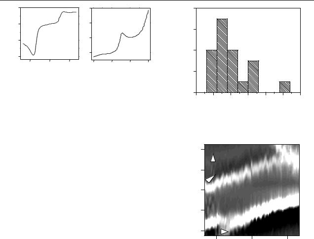
In a series of control experiments, electromigrated control samples that were exposed to various solvents (e.g. THF, toluene, methyl chloride) prior to being placed in the vacuum probe station were thermally cycled multiple times over the course of three to five days. In 10% of 175 multiple thermal cycled control devices we observed regions of NDR in their ID–VD curves at 4.2 K, such as those shown in figure 6.
We suggest that the NDR results from sharp features in the densities of states of the source and drain electrodes due to adsorbed impurities. The role of unintended adsorbates seems clear, since the NDR tends to appear as surfaces are exposed for significant periods in non-UHV conditions. We believe that there is one particular kind of adsorbate that causes the NDR in our control devices. The evidence for our assertion is
|
8 |
|
Number |
6 |
|
4 |
||
|
||
|
2 |
|
|
0 |
50 100 150 200 250
VD for max. NDR [mV]
Figure 7. For VG = 0, the distribution of bias voltages at which maximum NDR occurs. The histogram is singly peaked, suggesting that a single specific mechanism is producing the NDR effect.
|
40 |
|
|
[mV] |
0 |
|
|
|
|
|
|
D |
|
|
|
V |
|
|
|
|
–40 |
|
|
|
–60 |
0 |
60 |
|
|
VG [V] |
|
Figure 8. The differential conductance map of a control device showing gateable NDR. The brightness runs from −8 × 10⁻⁸ S (black) to 2 × 10⁻⁷ S (white). The arrows indicate NDR regions.
shown in figure 7, a histogram of the bias position (at zero gate voltage) where the maximum NDR occurs for these devices. The histogram is peaked prominently near 75 mV, suggesting that the NDR in these devices has a well-defined, common origin, rather than being a random phenomenon.
Similarly to STS experiments where NDR were observed [51, 52], we also observe in these devices that NDR can appear in either only one or both bias directions. About 30% of the NDR devices exhibit NDR in both bias polarities. All devices that exhibit NDR in both bias directions are also gateable. The conductance map of such a device is shown in figure 8. Regions of NDR are indicated by the arrows.
The concurrency of NDR in both bias directions and the gateablity of the devices reflects the extended screening length in the metal–molecule junction when the apex of the electrode is weakly coupled to the bulk of the electrode. If the screening length is long enough for the emergence of a voltage drop between the apex and the bulk of the electrode, then it would likely be long enough for the gate to influence the electrostatic potential of the metal–molecule junction.
The fact that the nonlinear conduction can be modulated by VG even in the absence of a Coulomb blockade
S522

Transport in single-molecule transistors
strongly constrains alternative NDR explanations. For example, vibrationally mediated NDR sometimes observed in STS experiments on adsorbed molecules [30] is only expected to occur at biases that correspond to specific mechanical modes of the adsorbate. Since those vibrational modes are determined by molecular structure rather than electrostatics, gate-independent NDR would be expected from this mechanism. Similarly, the lack of correlation of NDR with Coulomb charging implies that the molecular orbital effects suggested [24] to explain some nanopore NDR observations [5] are not relevant.
Experiments are continuing to determine the particular adsorbates responsible for the NDR. As with the Kondo physics discussed above, a reliable method to create stable nanometrescale NDR devices with significant peak-to-valley ratios would have significant practical implications.
6. Summary
We have employed an electromigration technique to create three terminal devices with source and drain electrodes separated on the single nanometre scale. With these devices we have demonstrated single-molecule transistors based on C60 that operate as single-electron devices that can access two molecular charge states. Some of these C60 SMTs exhibit conductance properties consistent with Kondo physics. Kondo transport here is indicated by the presence of a zero-bias peak in the conductance for one SMT charge state, and a Coulomb blockade for the other. The role of C60 is indicated by resonance features in the conductance energetically compatible with known molecular vibrational modes. Because of the resonant nature of conduction in the Kondo regime, this physics holds out the promise of SMTs with a conductance
per molecule in the ‘on’ state approaching the theoretical maximum, 2e2/ h.
Control devices left exposed to non-UHV conditions demonstrate a propensity to exhibit negative differential resistance. We have shown that this NDR may be modulated via VG, and propose that its explanation lies in sharp peaks in the local densities of states of the source and drain electrodes due to adsorbed impurities. We argue that the peaked distribution of NDR voltage characteristics implies that a single type of impurity is responsible for this nonlinear conduction. An improved understanding of this system may allow the controlled engineering of molecule-scale NDR devices.
Acknowledgments
The authors thank K Kelly and A Osgood for STM characterization, and P L McEuen, P Nordlander, H Park, D C Ralph, A Rimberg, J M Tour, and R L Willett for useful conversations.
This work was supported by the Robert A Welch Foundation, the Research Corporation, the David and Lucille Packard Foundation, and the National Science Foundation.
References
[1]Aviram A and Ratner M 1974 Chem. Phys. Lett. 29 277–83
[2]Nitzan A and Ratner M 2003 Science 300 1384–9
[3]Tour J 2000 Acc. Chem. Res. 33 791–804
[4]Ralls K and Buhrman R 1988 Phys. Rev. Lett. 60 2434–8
[5]Chen J, Reed M A, Rawlett A M and Tour J M 1999 Science 286 1550
[6]Reed M A, Chen J, Rawlett A M, Price D W and Tour J M 2001 Appl. Phys. Lett. 78 3735–7
[7]Collier C, Wong E, Belohradsky M, Raymo F, Stoddart J, Keukes P, Williams R and Heath J 1999 Science 285 391–4
[8]Collier C, Mattersteig G, Wong E, Luo Y, Beverly K, Sampaio J, Raymo F, Stoddart J and Heath J 2000 Science 289 1172–5
[9]Kushmerick J, Holt D, Yang J, Naciri J, Moore M and Shashidar R 2002 Phys. Rev. Lett. 89 086802
[10]van Ruitenbeek J, Alvarez A, Pineyro˜ I, Grahmann C, Joyez P, Devoret M, Esteve D and Urbina C 1996 Rev. Sci. Instrum. 67 108–11
[11]Reed M, Zhou C, Muller C, Burgin T and Tour J 1997 Science 278 252–4
[12]Scheer E, Agra¨ıt N, Cuevas J C, Yeyati A L, Ludolph B, Martin-Rodero A, Bollinger G R, van Ruitenbeek J M and Urbina C 1998 Nature 394 154–7
[13]Reichert J, Ochs R, Beckmann D, Weber H, Mayor M and von Lohneysen H 2002 Phys. Rev. Lett. 88 176804
[14]Smit R, Noat Y, Untiedt C, Lang N, van Hemert M and
van Ruitenbeek J 2002 Nature 419 906–9
[15]Joachim C, Gimzewski J, Schlittler R and Chavy C 1995 Phys. Rev. Lett. 74 2102–5
[16]Yazdani A, Eigler D and Lang N 1996 Science 272 1921–4
[17]Datta S, Tian W, Hong S, Reifenberger R, Henderson J I and Kubiak C P 1997 Phys. Rev. Lett. 79 2530–3
[18]Stipe B, Rezaei M and Ho W 1998 Science 280 1732–5
[19]Donhauser Z J, Mantooth B A, Kelly K F, Bumm L A, Monnell J D, Stapleton J J, Price D W Jr, Rawlett A M, Allara D K, Tour J M and Weiss P S 2001 Science 292 2303–7
[20]Ramachandran G, Hopson T, Rawlett A, Nagahara L,
Primak A and Lindsay S 2003 Science 300 1413–6
[21]Wold D and Frisbie C 2001 J. Am. Chem. Soc. 123 5549–56
[22]Cui X D, Primak A, Zarate X, Tomfohr J, Sankey O F, Moore A L, Moore T A, Gust D, Harris G and Lindsay S M 2001 Science 294 571–4
[23]Metzger R, Chen B, Hopfner¨ U, Lakshmikantham M, Vuillaume D, Kawai T, Wu X, Tachibana H, Hughes T, Sakurai H, Baldwin J, Hosch C, Cava M, Brehmer L and Ashwell G 1997 J. Am. Chem. Soc. 119 10455–66
[24]Seminario J, Zacarias A and Tour J 2000 J. Am. Chem. Soc. 122 3015–20
[25]Seminario J, Zacarias A and Derosa P 2001 J. Phys. Chem. A 105 791–5
[26]Seminario J, Zacarias A and Tour J 1998 J. Am. Chem. Soc. 120 3970–4
[27]Emberly E and Kirczenow G 2001 Phys. Rev. B 64 125318
[28]Solak A, Ranganathan S, Itoh T and McCreery R 2002
Electrochem. Solid State Lett. 5 E43–6
[29]Troisi A and Ratner M 2002 J. Am. Chem. Soc. 124 14528–9
[30]Gaudioso J, Lauhon L and Ho W 2000 Phys. Rev. Lett. 85 1918–21
[31]Kuznetsov A and Ulstrup J 2002 J. Chem. Phys. 116 2149–65
[32]Troisi A, Ratner M and Nitzan A 2003 J. Chem. Phys. 118 6072–82
[33]Park H, Park J, Lim A, Anderson E, Alivisatos A and McEuen P 2000 Nature 407 57–60
[34]Park J, Pasupathy A N, Goldsmith J I, Chang C, Yaish Y, Petta J R, Rinkowski M, Sethna J P, Abruna˜ H D, McEuen P L and Ralph D C 2002 Nature 417 722–5
[35]Liang W, Shores M P, Bockrath M, Long J R and Park H 2002
Nature 417 725–9
[36]Park J, Pasupathy A, Goldsmith J, Soldatov A, Chang C, Yaish Y, Sethna J, Abruna˜ H, Ralph D and McEuen P 2003
Thin Solid Films 438/439 457–61
S523

L H Yu and D Natelson
[37]Kubatkin S, Danilov A, Hjort M, Cornil J, Bredas´ J L, Stuhr-Hansen N, Hedegård P and Bjornholm T 2003 Nature 425 698–701
[38]Yu L H and Natelson D 2004 Nano Lett. 4 79–83
[39]Yu H, Luo Y, Beverly K, Stoddart J, Tseng H R and Heath J 2003 Angew. Chem. Int. Edn Engl. 42
5706–11
[40]Park H, Lim A K L, Alivisatos A P, Park J and McEuen P L 1999 Appl. Phys. Lett. 75 301–3
[41]Grabert H and Devoret M H (ed) 1992 Single Charge Tunneling: Coulomb Blockade Phenomena in Nanostructures (NATO ASI Series B: Physics vol 294) (New York: Plenum)
[42]Zhitenev N B, Meng H and Bao Z 2002 Phys. Rev. Lett. 88 226801
[43]Goldhaber-Gordon D, Shtrikman H, Mahalu D,
Abusch-Magder D, Meirav U and Kastner M 1998 Nature
391 156–9
[44]Cronenwett S, Oosterkamp T and Kouwenhoven L 1998
Nature 281 540–4
[45]Kondo J 1964 Prog. Theor. Phys. 32 37–49
[46]Madhavan V, Chen W, Jamneala T, Crommie M and Wingreen N 1998 Science 280 567–9
[47]Madhavan V, Chen W, Jamneala T, Crommie M and Wingreen N 2001 Phys. Rev. B 64 165412
[48]Gores¨ J, Goldhaber-Gordon D, Heemeyer S, Kastner M, Shtrikman H, Mahalu D and Meirav U 2000 Phys. Rev. B 62 2188–94
[49]Esaki L 1958 Phys. Rev. 109 603–4
[50]Sollner T, Goodhue W, Tannenwald P, Parker C and
Peck D 1983 Appl. Phys. Lett. 43 588–90
[51]Lyo I and Avouris P 1989 Science 243 1369–71
[52]Xue Y, Datta S, Hong S, Reifenberger R, Henderson J and Kubiak C 1999 Phys. Rev. B 59 R7852–5
[53]Lang N 1997 Phys. Rev. B 55 9364–6
[54]Moskovits M, Tay L L, Yang J and Haslett T 2002 Top. Appl. Phys. 82 215–27
[55]Kelly K, Sarkar D, Hale G, Oldenburg S and Halas N 1996
Science 273 1371–3
[56]Likharev K 1999 Proc. IEEE 87 606–32
S524