

nanotechnology / nano4_7_052
.pdfINSTITUTE OF PHYSICS PUBLISHING |
NANOTECHNOLOGY |
Nanotechnology 15 (2004) S452–S458 |
PII: S0957-4484(04)73701-0 |
Observed suppression of room temperature negative differential resistance in organic monolayers on Si(100)
N P Guisinger, R Basu, M E Greene, A S Baluch and M C Hersam1
Department of Materials Science and Engineering, Northwestern University, 2220 Campus
Drive, Evanston, IL 60208-3108, USA
E-mail: m-hersam@northwestern.edu
Received 15 December 2003
Published 17 May 2004
Online at stacks.iop.org/Nano/15/S452
DOI: 10.1088/0957-4484/15/7/052
Abstract
The ultrahigh vacuum scanning tunnelling microscope was used to probe charge transport through two different organic monolayers adsorbed on the Si(100) substrate at room temperature. I –V measurements were taken on monolayers of 2,2,6,6-tetramethyl-1-piperidinyloxy (TEMPO) and cyclopentene for degenerately doped n-type and p-type substrates. Initial
I –V measurements for transport through the TEMPO monolayer exhibited a suppression of negative differential resistance (NDR) relative to previously reported charge transport through isolated molecules. I –V measurements were also performed on isolated cyclopentene molecules and cyclopentene monolayers. Similarly to TEMPO monolayers, the cyclopentene monolayers exhibited attenuated NDR behaviour relative to isolated molecules. The observed NDR suppression suggests that the high packing density of organic monolayers influences charge transport through molecule–semiconductor junctions.
1. Introduction
Over the past forty years, the microelectronics industry has been able to keep pace with Moore’s law, which predicted that the number of transistors per chip would grow exponentially with time [1]. Industry success can be attributed to several advances in a technology that focuses on a top-down approach to miniaturizing electronic devices. However, this approach is facing several foreseeable limitations that may result in alternative electronic strategies for sustaining Moore’s law in the decades to come [2]. Historically, the heavy demands on metal–oxide–semiconductor (MOS) technology as it is scaled to the deep submicron level were predicted in 1974 by Dennard and co-workers [3]. In that same year, Aviram and Ratner suggested an alternative strategy based on the electronic properties of individual molecules, which ultimately burgeoned into the modern field of molecular electronics [4].
1 Author to whom any correspondence should be addressed.
Several research efforts have identified molecular electronics as promising for providing high density storage and computation. Most of the success in this field has focused on the electrical properties of organic molecules between metal electrodes [5–17]. Concurrently, other research efforts have focused on the chemistry of covalently linking organic molecules to semiconductor surfaces [18]. Our research combines these two approaches by investigating charge transport through organic molecules directly bound to a semiconductor substrate. Organic molecules on semiconductor substrates present opportunities for novel molecular electronic charge transport mechanisms and are potentially compatible with conventional MOS technology.
Negative differential resistance (NDR) has recently been observed in I–V measurements for transport through individual organic molecules bound to degenerately doped Si(100) [19]. These measurements were taken while probing individual organic molecules at room temperature with an ultrahigh vacuum (UHV) scanning tunnelling microscope
0957-4484/04/070452+07$30.00 © 2004 IOP Publishing Ltd Printed in the UK |
S452 |

Observed suppression of room temperature NDR in organic monolayers on Si(100)
(STM). The bias polarity of the NDR was reported to be a strong function of the substrate doping type. Specifically, NDR was observed at negative sample bias for degenerately doped n-type Si(100) and at positive sample bias for degenerately p-type doped Si(100). The proposed mechanism for the observed NDR behaviour involves resonant tunnelling of the narrow band of free carriers in the Si(100) substrate through the discrete molecular orbitals of the covalently bound organic molecule, which is uniquely different from previously reported measurements observing NDR [20–28]. For a more detailed description of these silicon-based molecular resonant tunnelling experiments, we refer the reader to the original paper by Guisinger et al [19]. In addition, the theoretical model predicting the observed NDR for transport through organic molecules bound to Si(100) has been outlined in detail by Rakshit et al [29].
In this paper, we expand the previous study focused on individual molecules by investigating charge transport through an organic monolayer bound to a Si(100) substrate. UHV STM measurements on full organic monolayers provide insight into the role that the local environment plays in charge transport through molecule–semiconductor junctions. In addition, a full organic monolayer is a system more conducive to device fabrication and integration than individual molecules.
In this study, we utilize the UHV STM for characterization and I–V measurements on two organic monolayers chemisorbed on degenerately doped n-type and p-type Si(100). Initially, we probe an organic monolayer consisting of free radical 2,2,6,6,-tetramethyl-1-piperidinyloxy (TEMPO) molecules, which exhibited multiple NDR events in previously reported single-molecule I–V measurements [19]. Subsequently, we describe cyclopentene adsorbed on Si(100), where I–V measurements are reported for transport through individual molecules and full monolayers. In both systems, a suppression of the NDR peaks is observed in I–V measurements for transport through the full monolayers relative to measurements on single molecules. This paper concludes with a discussion of possible explanations of the observed data.
2. Experimental details
All experiments were performed in a custom-built room temperature UHV STM chamber, which maintains a base pressure less than 5 × 10⁻¹¹ Torr. The scanner is based on the Lyding design and is controlled by digital feedback electronics [30]. The UHV system is comprised of a sample preparation chamber and a chamber housing the STM scanner, which are isolated by a gate valve to minimize crosscontamination. An external gas manifold houses the molecular species, which are introduced into the STM chamber via one of two independent leak valves. The reported molecular doses are measured with an ion gauge.
The TEMPO and cyclopentene molecules were commercially purchased from Sigma-Aldrich without further purification. Both molecules are stable at room temperature and possess sufficient volatility to be leaked into the UHV chamber. The molecules themselves are loaded into custom-designed glass vials under the following procedure. The glass vials
undergo a cleaning in de-ionized water and soap detergent followed by solvent rinses in acetone and isopropyl alcohol. The vial is dried with nitrogen between the solvent cleanings. The Teflon stopper, which seals the vial, only undergoes the detergent wash followed by an isopropyl alcohol rinse. After the solvent cleaning, the assembled vial is loaded onto the chamber manifold and is pumped down with a mechanical pump followed by a turbo-pump for several minutes. This procedure helps to ensure that all the moisture is removed from the vial. In addition, the exterior of the vial is carefully heated with a propane torch while under vacuum to further remove moisture and unwanted residual organics from the interior of the vial. Once the vial has cooled, it is purged with nitrogen to a slight overpressure and sealed. The vial is now ready to be loaded with the molecules of interest. The loading procedure is accomplished in a Vacuum Atmospheres Company Nexus model nitrogen controlled glove box, which maintains oxygen and water levels to less than 1 ppm. After loading, the vial is returned to the UHV chamber manifold. Prior to dosing, the loaded vials undergo a series of freeze–pump–thaw cycles with liquid nitrogen.
The substrates used in all experiments were Virginia Semiconductor Si(100) degenerately n-type doped with arsenic to a resistivity of <0.005 cm or degenerately p-type doped with boron to a resistivity of <0.005 cm. To achieve an atomically pristine surface, the sample was flashed in the preparation chamber to a temperature of 1250 ◦ C for 30 s which resulted in a clean surface with a 2 × 1 reconstruction. Following surface preparation, the sample was characterized with STM prior to molecular dosing. All imaging was performed in constant current mode with a sample bias of ±2 V relative to a grounded tip and a set-point current of 0.1 nA. The STM tip was electrochemically etched from high temperature annealed W wire (1600 ◦ C for 48 h).
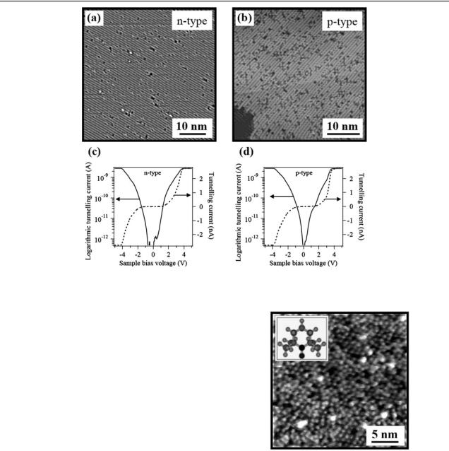
Characterization of the clean n-type Si(100) surface revealed an apparently high concentration of A-type, B-type and C-type surface defects [31], as illustrated in the filled states topographic STM image of figure 1(a). The p-type Si(100) sample also exhibited a high concentration of boron surface dopants as illustrated in the filled states topographic STM image of figure 1(b). The observed higher density of surface dopants on the p-type sample relative to the n-type sample is consistent with previous STM observations where it was noted that boron more readily segregates to the Si(100) surface under high temperature processing in UHV [32–34].
In addition to surface characterization, I–V measurements were taken on the clean surface with the STM. Figure 1(c) contains an I–V curve taken for the degenerately doped n-type Si(100) sample. Due to the range of the voltage sweep and the magnitude of the measured current, the linear– linear plot (dotted curve) appears to indicate a misleadingly large band gap. However, on plotting the data on a log-linear plot (solid curve), the band gap is clearly seen to possess the correct magnitude, and the Fermi level is positioned in close proximity to the conduction band edge as expected for degenerate n-type doping. I–V measurements were also acquired on the clean p-type Si(100) sample as illustrated in figure 1(d). These data are plotted in the same manner and indicate that the Fermi level is at the valence band edge in this case. Upon close inspection of the log-linear I–V curves for both doping
S453
N P Guisinger et al
Figure 1. Filled states STM images of clean degenerate (a) n-type and (b) p-type Si(100) substrates and corresponding I –V measurements on the (c) n-type and (d) p-type substrates.
types, it appears that the band gap is narrower than the expected 1.1 eV for silicon, which can be explained by the presence of surface states [31]. These initial I–V measurements taken on the clean Si(100) surface serve as a control for comparison with I–V measurements taken for transport through organic molecules and monolayers bound to the same substrates.
In order to obtain full monolayer coverage, the optimal dose was 0.6 L (10−9 Torr for 10 min) and 60 L (10−7 Torr for 10 min) for TEMPO and cyclopentene respectively. Following molecular dosing, the sample was returned to the tunnelling range and imaged with the STM. Once piezo-creep and other sources of drift were minimized, the STM was used to take I–V spectra. In particular, several positions for I–V curves were preselected based on a preceding topographic STM image of the surface. A subsequent topographic scan was then initiated, and the I–V measurements were taken in real time in order to ensure an accurate assessment of the spatial position of each I–V curve. For each I–V measurement, the feedback was disengaged, and the sample voltage was swept from −5 to +5 V while the tunnelling current was recorded. During these experiments, the current preamplifier gain was set at 109 V A−1, which limits current measurements to a range of
±2.75 nA. Any current values exceeding this range result in saturation of the current preamplifier, as observed in some of the I–V measurements near the upper and lower bounds of the sweep voltage.
3. Experimental results
As previously mentioned, I–V measurements for transport through isolated TEMPO molecules exhibited NDR behaviour for binding to degenerately doped Si(100) [19], thus making it
Figure 2. A filled states STM image of a monolayer of TEMPO adsorbed on the n-type Si(100) substrate. The inset is a schematic depiction of the chemical structure of TEMPO.
an ideal candidate for monolayer study. Prior to taking charge transport measurements, the STM was used to characterize the quality of the TEMPO monolayer as illustrated in figure 2. From the STM image, it is clear that TEMPO is completely coating the Si(100) surface. Furthermore, from progressive dosing studies (not shown), it was verified that this surface contains a monolayer—as opposed to multiple layers—of TEMPO. The surface packing density of the TEMPO appears to have resulted in a complete loss of the 2 × 1 surface reconstruction inherent to clean Si(100). In addition, the TEMPO monolayer lacks any long range order on the surface. These observations are consistent with previous reports [35].
Following surface characterization with the STM, I–V measurements were made for transport through the TEMPO
S454
Observed suppression of room temperature NDR in organic monolayers on Si(100)
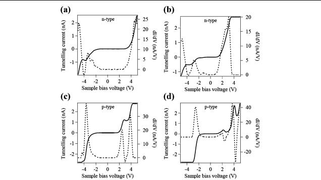
Figure 3. (a), (b) Representative I –V measurements taken on the TEMPO monolayer adsorbed on n-type Si(100) which exhibited NDR. (c), (d) Representative I –V measurements taken on the TEMPO monolayer adsorbed on p-type Si(100) which exhibited NDR behaviour. The dashed curves are the numerical derivatives of the current with respect to voltage (dI /dV ).
monolayer for both n-type and p-type substrates. Because of the complete surface coverage, I–V measurements could be rapidly obtained for transport through TEMPO molecules at essentially any point on the surface. In a typical measurement, a 40 nm × 40 nm STM image was taken to confirm surface quality, and then I–V curves were taken on a 10 × 10 grid of points evenly spaced by 4 nm. On average, approximately 30% of the I–V curves showed NDR for transport through the TEMPO monolayer.
In all cases on degenerately n-type doped Si(100), NDR occurred at negative sample bias in agreement with previously reported single-molecule measurements [19]. Figures 3(a),
(b) contain two representative examples of NDR data for the TEMPO monolayer on degenerately n-type doped Si(100). The solid curve is the I–V data, while the dashed curve is the numerical derivative (dI/dV ), which has been included to help visualize regions of abrupt change in the differential tunnelling conductance. Both of these I–V measurements show attenuated NDR behaviour in comparison to measurements made for transport through isolated molecules [19]. For example, there only appears to be one NDR event on the monolayer as opposed to the multiple peaks observed for transport through isolated TEMPO molecules. In addition, the peak to valley ratio of NDR events is significantly lower on the monolayer compared to isolated molecules.
I–V measurements were also made on a TEMPO monolayer bound to degenerately p-type doped Si(100). In this case, NDR is consistently observed at positive sample bias as illustrated by the two representative I–V curves of figures 3(c), (d). Although the polarity of the NDR is consistent with previous results for single TEMPO molecules on degenerate p-type Si(100) [19], the peak to valley
ratio is generally attenuated in monolayer measurements. Nevertheless, multiple NDR events are occasionally observed for TEMPO monolayers on degenerately p-type doped Si(100) as shown in figure 3(d).
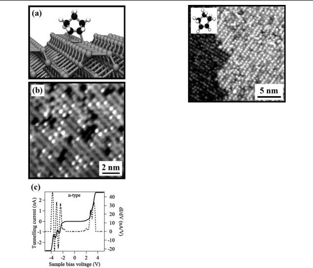
To investigate the effects of monolayer ordering on charge transport, a different organic molecule, cyclopentene, was chosen on the basis of its ability to form an ordered monolayer on Si(100) [36]. Another advantage of cyclopentene is that it is a fully saturated hydrocarbon once bound to the Si(100) surface as depicted in figure 4(a). The lack of π bonds for cyclopentene bound to Si(100) minimizes the likelihood of electron stimulated desorption [37–39], which is a necessary precondition for measurements of charge transport through molecule–semiconductor junctions.
Initial I–V measurements were taken on isolated cyclopentene molecules to ensure that NDR behaviour was occurring for this previously unstudied molecule. Figure 4(b) is a filled states STM image of a clean n-type Si(100) sample following exposure to a 0.02 L dose of cyclopentene. The isolated cyclopentene molecules appear as bright protrusions on the surface. Figure 4(c) shows an I–V measurement for transport through an isolated cyclopentene molecule on the degenerately n-type doped Si(100) surface, which clearly shows multiple NDR events at negative sample bias. Once again these results are consistent with previously observed charge transport through isolated molecules on degenerate n-type Si(100) [19]. An interesting feature of the I–V measurement is the presence of two discontinuities in the differential tunnelling conductance at positive sample bias, which are clearly visible in the numerical derivative. Single discontinuities have been observed in I–V measurements for transport through isolated TEMPO molecules and are
S455
N P Guisinger et al
Figure 4. (a) A schematic depiction of an individual cyclopentene molecule adsorbed on a silicon dimer on the Si(100) surface. (b) A filled states STM image of isolated cyclopentene molecules adsorbed on the n-type Si(100) substrate. (c) I –V measurements for transport through an isolated cyclopentene molecule exhibiting multiple NDR events at negative sample bias and multiple shoulders at positive sample bias. The dashed curve is the numerical derivative of the measured I –V .
attributed to the electrochemical potential of the tip aligning with the molecular orbitals [19].
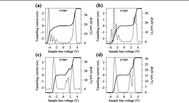
Full monolayer coverage of cyclopentene is illustrated in the filled states STM image of figure 5. The monolayer is highly ordered with the cyclopentene molecules aligned along the dimer rows of the Si(100) surface. Following the same procedure as described for TEMPO monolayers, several I–V measurements were taken on cyclopentene monolayers on degenerate n-type and p-type Si(100). As seen with TEMPO monolayers, approximately 30% of the I–V curves for cyclopentene monolayers exhibited NDR. Figures 6(a), (b) contain two representative I–V curves obtained for transport through the cyclopentene monolayer on the n-type sample. Once again, NDR is only observed at negative sample bias. Although multiple NDR events are occasionally observed on the cyclopentene monolayer, the overall NDR behaviour is
Figure 5. A filled states STM image of a molecular monolayer of cyclopentene adsorbed on the n-type Si(100) substrate. The inset is a schematic depiction of the chemical structure of cyclopentene.
greatly suppressed compared to the measurements for transport through isolated molecules, in agreement with charge transport measurements on the TEMPO monolayer. I–V measurements taken for transport through the cyclopentene monolayer bound to degenerately p-type doped Si(100) show similar behaviour to the n-type sample but at the opposite polarity, as illustrated in figures 6(c), (d).
4. Discussion
This paper has explored charge transport through two different organic monolayers bound to Si(100). Both TEMPO and cyclopentene monolayers exhibited NDR behaviour whose bias polarity was dictated by the substrate doping. This observation is consistent with the initial reports of NDR in molecule–semiconductor junctions [19]. The proposed mechanism for this behaviour [29] assumes that the molecular orbital levels are aligned in such a way that the electrochemical potential of the Si(100) substrate will move into tunnelling resonance with these levels under applied bias. In equilibrium, this assumption implies that the lowest unoccupied molecular orbital should be closely aligned with the conduction band edge of the n-type substrate, whereas the highest occupied molecular orbital should be closely aligned with the valence band edge of the p-type substrate. However, this alignment is difficult to accept when considering the molecular orbital positions of a molecule, such as cyclopentene, measured by gas phase ultraviolet photoemission spectroscopy (UPS) [40]. In charge transport measurements, though, the molecule is not in the gas phase but is chemically bound to the Si(100) surface. Previous reports of UPS spectra collected for cyclopentene bound to Si(100) indicate quenching of the Si(100) dangling bond states by the bound cyclopentene molecules in agreement with the schematic diagram of figure 4(a) [41]. In addition, recent reports provide evidence for charge transfer between organic molecules and the underlying Si(100) substrate, which would be likely to influence the position of the molecular orbitals [42, 43]. Doping dependent charge transfer is thus a plausible justification for the counter-intuitive orbital alignment that is necessary to provide consistency between the proposed mechanism and the experimental data.
The experimental results of this paper further showed that NDR appears to be greatly suppressed when measuring for
S456
Observed suppression of room temperature NDR in organic monolayers on Si(100)
Figure 6. (a), (b) Representative I –V measurements taken on the cyclopentene monolayer adsorbed on n-type Si(100) which exhibited NDR. (c), (d) Representative I –V measurements taken on the cyclopentene monolayer adsorbed on p-type Si(100) which exhibited NDR behaviour. The dashed curves are the numerical derivatives of the current with respect to voltage (dI /dV ).
transport through organic monolayers as opposed to isolated molecules. These results suggest that the local environment surrounding each molecule plays an important role in the charge transport. The most obvious change in the local environment for the monolayer compared to isolated molecules is the presence of other molecules in close proximity to the molecule under test. In an ideal scenario, all of the tunnelling current from the STM tip will pass through an individual molecule. However, especially for a densely packed monolayer where the intermolecular spacing is minimized, it is conceivable that tunnelling may concurrently occur through more than one molecule. Since the tip–sample spacing strongly dictates the voltage at which NDR is observed [29], concurrent tunnelling through more than one molecule with different tip–sample spacing for each molecule would lead to a superposition of offset NDR events. In the best case scenario, this would result in more NDR events than expected for an isolated molecule as observed in figures 6(a), (b). However, since not all of the tunnelling current is participating in resonant tunnelling, the NDR would also be greatly attenuated compared to the case where all of the tunnelling current is flowing through one molecule. This explanation agrees well with the consistent observation of suppressed NDR in organic monolayers compared to isolated molecules.
The minimal intermolecular spacing in densely packed monolayers may also lead to intermolecular interactions that would perturb the local molecular orbital alignment. If these intermolecular interactions were a large effect, then the charge transport is likely to be less uniform on a disordered monolayer, where the local environment would be more variable, than on an ordered monolayer. Qualitatively, our measurements do not show significant differences in uniformity between TEMPO and cyclopentene monolayers on Si(100) despite clear differences in the degree of ordering for these two
surfaces. These measurements suggest that intermolecular spacing rather than intermolecular ordering appears to be playing a dominant role in determining the charge transport through organic monolayers on Si(100). Consequently, the former mechanism of concurrent tunnelling through adjacent molecules appears more likely than local molecular orbital misalignment or broadening induced by a spatially varying intermolecular interaction.
Alternative explanations for the observed data may include the role of subsurface defects. From the initial images of the clean Si(100) surface, it is clear that there is a high density of surface defects present on the degenerately n-type and p- type doped substrates. In submonolayer studies of isolated molecules, these surface defects can generally be observed in STM images and avoided in subsequent charge transport measurements. However, on full monolayers, subsurface defects are typically masked by the monolayer. Consequently, they are not intentionally avoided and are likely to be present in many of the monolayer I–V curves. Nevertheless, it is exceedingly unlikely that they are present in all of our monolayer measurements, which implies that subsurface dopants are not the sole explanation of the observed differences between the monolayer and isolated molecule studies.
5. Conclusions
The UHV STM was utilized for the measurement of charge transport through two organic monolayers on Si(100). I–V measurements for transport through a TEMPO monolayer on both degenerate n-type and degenerate p-type Si(100) substrates exhibited a suppression of NDR behaviour compared to previously reported measurements taken for transport through isolated TEMPO molecules. In an effort to test the role of monolayer ordering in the observed suppression
S457

N P Guisinger et al
of NDR, cyclopentene, which is known to form a more ordered monolayer on Si(100), was also studied. Prior to studying full monolayer coverage, I–V measurements were performed for transport through individual cyclopentene molecules, which exhibited multiple NDR events consistent with prior observations of isolated TEMPO molecules. However, as with the TEMPO monolayer, measurements for charge transport through the cyclopentene monolayer exhibited a strong suppression of the NDR behaviour. Consequently, the packing of the monolayer—rather than the ordering of the monolayer—appears to be the dominant factor influencing the suppression of NDR.
Acknowledgments
We thank S Datta and his research group at Purdue University for fruitful discussions and theoretical guidance. This work was supported by an Arnold and Mabel Beckman Young Investigator Award, the NASA Institute for Nanoelectronics and Computing under Award Number NCC 2-3163, the Nanoscale Science and Engineering Initiative of the National Science Foundation under NSF Award Numbers EEC– 0118025 and DMR-0134706, and the Defense University Research Initiative in Nanotechnology of the United States Army Research Office under Grant Number DAAD 19-01- 1-0521. One of the authors (MEG) acknowledges support from the National Defense Science and Engineering Graduate Fellowship Program.
References
[1]Moore G E 1965 Electronics 38 114
[2]Lundstrom M 2003 Science 299 210
[3]Dennard R H, Gaensslen F H, Yu H, Rideout V L, Bassous E and LeBlanc A R 1974 IEEE J. Solid-State Circuits 9 256
[4]Aviram A and Ratner M A 1974 Chem. Phys. Lett. 29 257
[5]Reed M A, Zhou C, Muller C J, Burgin T P and Tour J M 1997
Science 278 252
[6]Zhou C, Deshpande M R, Reed M A and Tour J M 1997 Appl. Phys. Lett. 71 611
[7]Zhou C, Muller C J, Deshpande M R, Sleight J W and
Reed M A 1995 Appl. Phys. Lett. 67 1160
[8]Chen J, Reed M A, Rawlett A M and Tour J M 1999 Science 286 1550
[9]Chen J, Wang W, Reed M A, Rawlett A M, Price D W and Tour J M 2000 Appl. Phys. Lett. 21 1224
[10]Service R F 2001 Science 294 2442
[11]Andres R P, Bein T, Dorogi M, Feng S, Henderson J I, Kubiak C P, Mahoney W, Osifchin R G and Reifenberger R 1996 Science 272 1323
[12]Metzger R M 2000 J. Mater. Chem. 10 55
[13]Collier C P, Mattersteig G, Young E W, Luo Y, Beverly K, Sampaio J, Raymo F M, Stoddart J F and Heath J R 2000
Science 289 1172
[14]Donhauser Z J, Mantooth B A, Kelley K F, Bumm L A, Monnell J D, Stapleton J J, Price D W Jr, Rawlett A M, Allara D L, Tour J M and Weiss P S 2001 Science 292 2303
[15]Ramachandran G K, Hopson T J, Rawlett A M, Nagahara L A, Primak A and Lindsay S M 2003 Science 300 1413
[16]Park J, Pasupathy A N, Goldsmith J I, Chang C, Yaish Y, Petta J R, Rinkoski M, Sethna J P, Abruna˜ H D, McEuen P L and Ralph D C 2002 Nature 417 722
[17]Liang W, Shores M P, Bockrath M, Long J R and Park H 2002
Nature 417 725
[18]Buriak J M 2002 Chem. Rev. 102 1271
[19]Guisinger N P, Greene M E, Basu R, Baluch A S and
Hersam M C 2004 Nano Lett. 4 55
[20]Xue Y, Datta S, Hong S, Reifenberger R, Henderson J I and Kubiak C P 1999 Phys. Rev. B 59 R7852
[21]Fan F F, Yang J, Cai L, Price D W Jr, Dirk S M,
Kosynkin D V, Yao Y, Rawlett A M, Tour J M and Bard A J 2002 J. Am. Chem. Soc. 124 5550
[22]Lyo I-W and Avouris Ph 1989 Science 245 1369
[23]Bedrossian P, Chen D M, Mortensen K and Golovchenko J A 1989 Nature 342 258
[24]Ma D D D, Wang Y G, Lu L, Lee C S and Lee S T 2002 Appl. Phys. Lett. 80 1231
[25]Avouris Ph, Lyo I-W, Bozso F and Kaxiras E 1990 J. Vac. Sci. Technol. A 8 3405
[26]Johansson M K-J, Gray S M and Johansson L S O 1996 J. Vac. Sci. Technol. B 14 1015
[27]Yakabe T, Dong Z-C and Nejoh H 1997 Appl. Surf. Sci. 121 187
[28]Komura T, Yoshimura M and Yao T 1997 Japan. J. Appl. Phys. 36 4013
[29]Rakshit T, Liang G-C, Ghosh A W and Datta S 2003 Preprint cond-mat 0305695v1
[30]Lyding J W, Skala S, Hubacek J S, Brockenbrough R and Gammie G 1988 Rev. Sci. Instrum. 59 1897
[31]Hamers R J and Kohler U K 1989 J. Vac. Sci. Technol. A 7 2854
[32]Zhang Z, Kulakov M A, Bullemer B, Zotov A V and
Eisele I 1996 J. Vac. Sci. Technol. A 14 2684
[33]Kulakov M A, Zhang Z, Zotov A V, Bullemer B and Eisele I 1996 Appl. Surf. Sci. 103 443
[34]Komeda T and Nishioka Y 1998 Surf. Sci. 405 38
[35]Guisinger N P, Basu R, Baluch A S and Hersam M C 2003
Ann. N.Y. Acad. Sci. 1006 227
[36]Hovis J S, Liu H and Hamers R J 1998 Surf. Sci. 404 1
[37]Alavi S, Rousseau R, Patitsas S N, Lopinski G P,
Wolkow R A and Seideman T 2000 Phys. Rev. Lett. 85 5372
[38]Kruse P and Wolkow R A 2002 Appl. Phys. Lett. 81 4422
[39]Patitsas S N, Lopinski G P, Hul’ko O, Moffatt D J and Wolkow R A 2000 Surf. Sci. 457 L425
[40]Kimura K, Katsumata S, Achiba Y, Yamazaki T and
Iwata S 1981 Handbook of HeI Photoelectron Spectra of Fundamental Organic Molecules (Tokyo: Japan Scientific Societies Press)
[41] Yamashita R, Hamaguchi K, Machida S, Mukai K, Yoshinobu J, Tanaka S and Kamada M 2001 Appl. Surf. Sci.
169 172
[42]Hersam M C, Guisinger N P and Lyding J W 2000
Nanotechnology 11 70
[43]Akiyama R, Matsumoto T and Kawai T 2000 Phys. Rev. B 62 2034
S458