

INSTITUTE OF PHYSICS PUBLISHING |
NANOTECHNOLOGY |
Nanotechnology 16 (2005) 1482–1485 |
doi:10.1088/0957-4484/16/9/011 |
Silicon nanowires as enhancement-mode Schottky barrier field-effect transistors
Sang-Mo Koo, Monica D Edelstein, Qiliang Li, Curt A Richter and
Eric M Vogel
Semiconductor Electronics Division, National Institute of Standards and Technology (NIST),
100 Bureau Drive, Gaithersburg, MD 20899, USA
E-mail: smkoo@nist.gov
Received 22 April 2005
Published 29 June 2005
Online at stacks.iop.org/Nano/16/1482
Abstract
Silicon nanowire field-effect transistors (SiNWFETs) have been fabricated with a highly simplified integration scheme to function as Schottky barrier transistors with excellent enhancement-mode characteristics and a high on/off current ratio 107. SiNWFETs show significant improvement in the thermal emission leakage ( 6 × 10⁻¹³ A µm−1) compared to reference FETs with a larger channel width ( 7 × 10⁻¹⁰ A µm−1). The drain current level depends substantially on the contact metal work function as determined by examining devices with different source/drain contacts of Ti (≈4.33 eV) and Cr (≈4.50 eV). The different conduction mechanisms for accumulationand inversion-mode operation are discussed and compared with two-dimensional numerical simulation results.
1. Introduction
Recently, silicon nanowire (SiNW) devices have received considerable attention as regards use in integrated nanoscale electronics [1, 2] as well as for studying fundamental properties in small dimensions [3]. To realize reliable devices or test structures at nanoscale dimensions, key issues must be addressed including accurate control of the doping level of the SiNW and the formation of reliable metal contacts. Among a number of works reported [4, 5], in most of the experimental works SiNW devices were fabricated using the ‘bottom-up’ approach, which often encounters difficulties in controlling the doping and contact properties of SiNWs [1, 4]. SiNW devices fabricated using the ‘top-down’ approach show better control and reproducibility in these parameters, but the main focus has been on traditional field-effect transistor (FET) structures with n–p–n doping, which requires complex process steps to form the source and drain doping and metal contacts [6, 7]. In this work, we demonstrate that SiNWs with Schottky contacts can be used as enhancement-mode FETs. Schottky barrier FETs are of great interest on their own account as an alternative to traditional doped source and drain device structures, because sub-100 nm range scaling encounters fundamental problems including high leakage current and parasitic resistance [8, 9]. Schottky barrier FETs have a number of advantages including simple and low temperature processing, good suppression
of short channel effects, and the elimination of doping and subsequent activation steps. These features are particularly desirable for SiNW devices because they can circumvent difficult fabrication issues such as an accurate control of the doping type/level and the formation of reliable ohmic contacts. However, there is no reported work on SiNW device structures explored as Schottky barrier FETs. Here we show that SiNWs with Schottky contacts can be used as enhancement-mode FETs with an excellent on/off current ratio. The process does not require any source and drain doping or silicide formation, thereby allowing for a simple process without thermal annealing. The effect of the contact metal work functions on the device properties and the different conduction mechanisms for both accumulation and inversion channels are discussed and compared with numerical simulation results.
2. Device fabrication
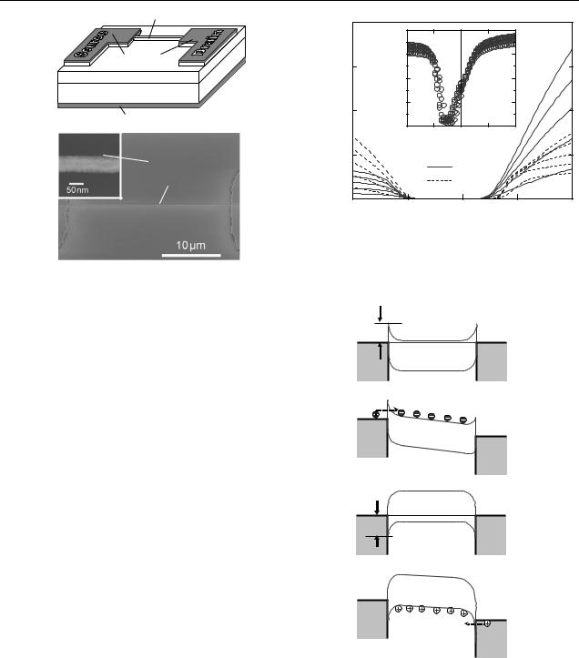
Figure 1(a) shows a schematic diagram of the fabricated SiNWFET structure. The starting materials used were (100) oriented silicon-on-insulator (SOI) wafers, which have a 50 nm thick SOI layer on top of 100 nm thick thermally grown buried oxide (BOX). Both the SOI layer and the substrate are p- type with a boron doping of 2 × 1015 cm−3. To fabricate the SiNWFET, the source and drain metal electrodes were formed by evaporating first Ti or Cr and then Au onto the
0957-4484/05/091482+04$30.00 © 2005 IOP Publishing Ltd Printed in the UK |
1482 |
Si NWs as enhancement-mode Schottky barrier FETs
(a)Si Nanowire Channel
Au/Cr or Au/Ti
BOX
|
Si Substrate |
|
Gate |
(b) |
|
|
Si Nanowire |
|
Channel |
Source |
Drain |
Figure 1. (a) Schematic diagram of the SiNWFET. (b) Scanning electron microscopy (SEM) images of the nanowire channel.
|
4.0x10⁻⁷ |
10-6 |
|
VD=0 to 1 V, 0.2 V per step |
|
|
|
|
|
|
|
|
3.0x10⁻⁷ |
|
|
|
|
(A) |
2.0x10⁻⁷ |
|
|
|
|
|
|
|
|
|
|
D |
|
|
|
|
|
I |
|
|
|
|
|
|
1.0x10⁻⁷ |
|
|
|
|
|
|
|
Au/Ti |
|
|
|
|
|
Au/Cr |
|
|
|
0.0 |
|
|
|
|
|
-10 |
-5 |
0 |
5 |
10 |
|
|
|
VG (V) |
|
|
Figure 2. Drain current ID versus gate voltage VG characteristics of SiNWFETs measured at room temperature for different source and drain metals, Au/Cr and Au/Ti. The inset shows the same data with the drain current plotted on a log scale.
SOI layer. The metal electrodes were further defined by a photolithography and etch process. The SiNW channel was then patterned between the source and drain metals by electron beam lithography (EBL). Reactive ion etching (RIE) defines the SiNW channel together with the source and drain areas. There is no additional doping step for the source/drain region and no subsequent thermal annealing was applied. In this process, the source and drain electrodes act as both alignment marks for EBL and self-aligned masks for the RIE. Thus the device structure can be formed with minimal process steps and without high temperature processes. The SiNWFETs reported here have channel widths of 60 nm and channel length of 28 µm. FETs with larger channel widths up to 5 µm have been simultaneously fabricated as reference devices. Scanning electron microscopy (SEM) images of SiNW channels are shown in figure 1(b). The BOX/Si substrate gate can be biased to form a conducting channel in the SOI layer and both inversion and accumulation channels can be formed depending on the gate bias.
|
ΦBn |
|
|
(a) |
|
|
VD = 0 |
|
Source |
VG > 0 |
Drain |
|
|
|
|
(b) |
|
|
|
|
Source |
|
VD > 0 |
|
VG > 0 |
|
|
|
|
Drain |
|
|
|
|
|
(c) |
ΦBp |
VG < 0 |
VD = 0 |
|
|
|
|
|
Source |
|
Drain |
3. Characterization results and discussion
Figure 2 shows typical gate transfer characteristics (drain current ID versus gate voltage VG) for the SiNWFETs. Two different source and drain metals, Cr and Ti, have been investigated and compared. It was observed by making measurements on more than 20 different devices that the levels of the saturation current and the off state current are different for Cr and Ti, as shown in figure 2. The VG was scanned from 0 to either +10 or −10 V for different drain voltages (VD = 0– 1 V). The devices show so-called ambipolar characteristics with both p- and n-type conductions depending on the gate bias. The band diagrams along the nanowire channel from source to drain, for different bias conditions, are shown schematically in figure 3. It is known that a Schottky barrier occurs when metal is directly contacted to low doped silicon. At high gate voltages (|VG| > 0), which turn the device to the ‘on state’, the
(d)
VG < 0
Source |
VD > 0 |
|
Drain
Figure 3. Band diagrams along the nanowire channel from source to drain for different bias conditions: (a) positive gate bias VG > 0 without drain bias VD = 0, (b) positive gate bias and positive drain bias VD > 0, (c) negative gate bias VG < 0 without drain bias
VD = 0, and (d) negative gate bias and positive drain bias VD > 0. The barrier height between the metal and the p-type silicon nanowire is φBp. The barrier height for electrons when the channel is inverted is φBn.
electrons or holes may tunnel through the barrier as the width of the barrier decreases. For a positive gate bias (VG > 0), the electron barrier height φBn becomes sufficiently low and the thickness of the barrier decreases so that an inversion
1483
S-M Koo et al
electron channel can be formed and the channel is turned on with electron-dominant conduction (see figures 3(a) and (b)). On the other hand, an accumulation channel is formed for a negative gate bias (VG < 0), since the hole barrier height φBp is low and the barrier width becomes thin enough for the drain current to flow. In this case, the hole conduction dominates, as shown in figures 3(c) and (d).
Ideally, φBn can be expressed as φM − χ , where φM is the metal work function and χ is the electron affinity of Si (χ ≈ 4.05 eV), and φBp = Eg − φBn, where Eg is the bandgap of Si (Eg ≈ 1.12 eV) [10]. By using the work function values φM for Cr and Ti as 4.50 and 4.33 eV, respectively [11], φBn can be estimated as 0.45 eV for Cr and 0.28 eV for Ti, and φBp as 0.67 eV for Cr and 0.84 eV for Ti. In actual cases, interface states between metal and Si may affect the barrier heights and there are a range of reported values for φM as well as χ . For example, χ up to 4.29 eV is reported for Si [12] and the φM for Cr (3.6–4.33 eV) and Ti (3.9–4.65 eV) varies depending on the experimental method, the surface condition and the film thickness [13, 14]. Nevertheless, a relative barrier height difference between Cr/Si and Ti/Si can still be considered to be ≈0.2 eV in reasonable consistency with the literature.
As shown in figure 2, electron conduction is suppressed using Cr contacts relative to Ti contacts due to its higher φBn ( 0.45 eV) compared to that of Ti ( 0.28 eV). Accordingly, the hole conduction is enhanced for Cr due to the lower φBp of Cr ( 0.67 eV) compared to Ti ( 0.84 eV). For low gate bias voltages (VG 0), which correspond to the ‘off state’, the drain current ID is very small since the drain conduction is limited by the barrier height of the metal source and drain contact. The off state drain leakage, IOFF, is lower for Ticontacted SiNWFETs ( 6× 10⁻¹³ A µm−1 at VD = 1 V) than for Cr-contacted devices ( 7 × 10⁻¹⁰ A µm−1 at VD = 1 V) due the higher φBp of Ti. This leakage is mainly due to the thermionic emission of carriers across the barriers. The thermionic current level is related to the Schottky barrier height as I exp(−qφB/ kT ), where q is the electronic charge, k is the Boltzmann constant and T is the absolute temperature in kelvins. From this equation and the measured ratio (IOFF for Cr)/(IOFF for Ti), the barrier height difference between Cr/Si and Ti/Si in the SiNWFETs can be estimated to be ≈0.18 eV, which is in close agreement with the ideal calculation from the reported value (0.84–0.67 = 0.17 eV).
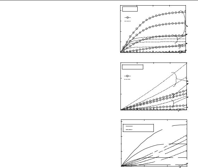
The measured drain current ID versus drain voltage VD characteristics of SiNWFETs are shown in figures 4(a) and
(b) for different source and drain metals, Cr and Ti. All the devices show enhancement-mode operation for both positive and negative gate biases. However, the SiNWFETs exhibit well-saturated drain conduction for inversion channels (VG > 0), whereas non-saturated drain current has been observed for accumulation channels (VG < 0).
For the case of electron-dominated conduction at high enough positive gate biases (VG > 0), the Schottky barrier width at the drain side slightly increases as VD increases. Thus, as VD further increases, the extra voltage drop appears mostly across the laterally expanding Schottky barrier on the drain side. Therefore, the voltage drop across the channel remains constant and equal to the saturation drain voltage. So the device behaves as an enhancement FET with well-saturated drain currents. On the other hand, when the device is in
(a) |
|
|
|
|
|
|
|
4.0x10 |
-7 |
Inversion |
|
VG=0 to 10 V, 2V/Step |
|
|
|
|
|
|
|
|
|
|
|
Measurements: |
|
|
|
(A) |
3.0x10⁻⁷ |
Au/Ti |
|
|
VG= |
|
Au/Cr |
|
|
||||
D |
|
|
|
|
|
|
I |
|
|
|
|
|
10, |
Measured |
|
|
|
|
|
|
2.0x10 |
-7 |
|
|
|
8, |
|
|
|
|
|
6 V |
||
|
|
|
|
|
||
1.0x10⁻⁷ |
|
|
|
4 V |
||
|
|
|
|
|
|
|
|
0.0 |
|
|
|
2, 0 V |
|
|
|
|
|
|
||
|
0.0 |
0.5 |
1.0 |
1.5 |
2.0 |
|
(b) |
3.0x10⁻⁷ |
|
VD (V) |
|
||
|
|
|
|
|
||
|
|
|
Accumulation |
VG=0 to -10 V, -2V/Step |
|
|
|
|
Measurements: |
|
|
VG= |
(A) |
2.0x10⁻⁷ |
Au/Ti |
|
|
|
Au/Cr |
|
|
-10, |
||
D |
|
|
|
|
-8 V |
I |
|
|
|
|
|
Measured |
|
|
|
|
|
1.0x10⁻⁷ |
|
|
|
-6 V |
|
|
|
|
|
|
|
|
|
|
|
|
-4, |
|
0.0 |
|
|
|
-2, |
|
0.5 |
1.0 |
1.5 |
0 V |
|
|
0.0 |
2.0 |
|||
(c) |
|
|
VD (V) |
|
|
|
2.4x10⁻⁶ |
Simulations: |
|
|
|
|
|
Inversion |
|
VG= 2.5 |
|
m) |
|
Accumulation |
|
|
|
1.6x10⁻⁶ |
|
|
|
|
|
(A/ |
|
|
|
|
|
|
|
|
|
|
|
D |
|
|
|
|
|
I |
|
|
|
2.0 |
|
Simulated |
|
|
|
|
|
8.0x10⁻⁷ |
|
|
-2.0 |
|
|
|
-1.5 |
|
|
||
|
|
-1.0 |
|
||
|
|
|
1.5 |
|
|
|
|
|
|
|
|
|
|
|
-0.5 |
0, 0.5 V |
|
|
0.0 |
|
|
1.0 |
|
|
|
|
|
|
|
|
0.0 |
0.7 |
|
1.4 |
|
|
|
|
VD (V) |
|
|
Figure 4. Drain current ID versus drain voltage VD characteristics of SiNWFETs measured at room temperature for different source and drain metals: (a) inversion (VG 0) and (b) accumulation (VG 0). The results from numerical simulation for both inversion and accumulation are compared in (c).
accumulation (VG < 0), the width of the Schottky barrier at the drain becomes thinner with increased drain biases. As the barrier has become thin enough for tunnelling, the increased voltage drop appears to be mainly in the channel rather than across the barrier. The accumulated holes are more abundant from the boron-doped starting material compared to the electron concentration in inversion and the holes having different tunnelling behaviours results in an increasing ID without saturation.
We have simulated the FET structure by using a twodimensional numerical simulator, ISE-TCAD [15], to further examine this effect. In figure 4(c), the drain characteristics of both electron (inverted)- and hole (accumulated)-dominant conduction are shown. Since our main focus is on the drain current saturation effect, we assumed a simple geometry without considering the work functions of different metals. Any secondary effects, which may present in the real case, such as interface states and fixed oxide charge are disregarded.
1484

Si NWs as enhancement-mode Schottky barrier FETs
Note also that in a real device, the bias applied to the gate may partly drop across the substrate and chuck and thus the gate bias levels may differ from the measurements. However, it is clearly observed in figure 4(c) that the drain saturation occurs not for the accumulation, but only for the electron inversion current, which further validates the experimental results and the conduction mechanisms discussed in this work. The effective channel mobility values for SiNWFETs with Ti electrodes are estimated to be around 650 and 330 cm2 V−1 s−1 for inversion and accumulation conduction, respectively, which are comparable to those reported for typical SOI devices of larger dimension [16]. An enhancement in the inversion layer mobility has been observed previously in n–p–n channel SiNWFETs [17]. Due to uncertainty of the SiNW dimensions extracted from the top-view of SEM images, it cannot be determined whether a similar enhancement is present in the SiNWFETs reported here when compared to simultaneously fabricated large area reference devices.
However, the on/off current ratio, ION/IOFF, is found to increase as the channel width (W ) of the SiNWFETs decreases. For example, Ti-contacted SiNWFETs with W = 60 nm exhibit about three-order-higher on/off drain current ratio ( 107) compared with the reference FETs, with W =
5 µm ( 104). The off current density IOFF is significantly reduced in SiNWFETs ( 6×10⁻¹³ A µm−1 at VD = 1 V, W =
60 nm) compared to the reference FETs with wider channel widths ( 2 × 10⁻¹⁰ A µm−1 at VD = 1 V, W = 5 µm). It has also been observed that the on/off ratio increases as the channel width decreases from the measurement data for a number of channel widths (W = 60 nm, 150 nm, 500 nm and 5 µm), which will be discussed in further detail elsewhere. This suggests that when the channel is scaled down to the nanoscale regime, the ultranarrow body of the channel significantly reduces the leakage paths that are primarily associated with possible defect states in Si.
4. Conclusion
In summary, SiNWFETs have been fabricated to function as Schottky barrier transistors and excellent enhancement-mode
ambipolar characteristics with high on/off current ratios of107 are demonstrated. The thermal emission leakage IOFF is significantly reduced in SiNWFETs ( 6 × 10⁻¹³ A µm−1) compared to the reference FETs with wider channel widths up to 5 µm ( 7 × 10⁻¹⁰ A µm−1). SiNWFETs exhibited ambipolar conduction, where the drain current level depends substantially on the contact metal work function. The high on/off current ratio of the proposed structure, together with its very simple process, may offer potential advantages for developing integrated nanoscale electronics as well as for studying fundamental properties in small dimensions.
Acknowledgments
The authors would like to thank David G Seiler, David L Blackburn, Eric K Lin and Erik M Secula for careful readings of the manuscript. The authors acknowledge the support of the NIST Office of Microelectronics Program and NIST Semiconductor Electronics Division.
References
[1]Cui Y and Lieber C M 2001 Science 291 851
[2]Mathur N 2002 Nature 419 573
[3]Xiao M et al 2004 Nature 430 435
[4]Cui Y et al 2003 Nano Lett. 3 149
[5]Ma D D D et al 2003 Science 299 1874
[6]Allibert F et al 2001 Solid State Electron. 45 559
[7]Hu S F et al 2004 IEEE Trans. Nanotechnol. 3 93
[8]Fritze M et al 2004 IEEE Electron Device Lett. 25 220
[9]Jang M et al 2003 Appl. Phys. Lett. 83 2611
[10]Sze S M 1981 Physics of Semiconductor Devices (New York: Wiley)
[11]CRC Handbook of Chemistry and Physics 2004 85th edn (Boca Raton, FL: CRC Press)
[12]Michaelson H B 1977 J. Appl. Phys. 48 4279
[13]Collins G S and Zacate M O 2003 Hyperfine Interact. 151/152 77
[14]Wilson R G 1966 J. Appl. Phys. 37 2261
[15]ISE-TCAD DESSIS User’s Guide Version 10.0 2004 (Zurich,¨ Switzerland: Integrated Systems Engineering)
[16]Cristoloveanu S, Munteanu D and Liu M S T 2000 IEEE Trans. Electron Devices 47 1018
[17]Koo S-M et al 2004 Nano Lett. 4 2197
1485