

nanotechnology / nano6_1_023.!!pdf
.pdfINSTITUTE OF PHYSICS PUBLISHING |
NANOTECHNOLOGY |
Nanotechnology 17 (2006) 145–151 |
doi:10.1088/0957-4484/17/1/023 |
Memory effect in thin films of insulating polymer and C60 nanocomposites
S Paul, A Kanwal and M Chhowalla1
Materials Science and Engineering, Rutgers University, 607 Taylor Road, Piscataway,
NJ 08854, USA
E-mail: manish1@rci.rutgers.edu (M Chhowalla)
Received 9 August 2005, in final form 3 October 2005
Published 1 December 2005
Online at stacks.iop.org/Nano/17/145
Abstract
We describe the use of C60 fullerene molecules as the charge storage medium in an insulating poly-vinyl-phenol (PVP) polymer. The simple metal–organic–metal (MOM) sandwich structure devices deposited from solution exhibit distinct high and low conduction states, which can be used to program read, write and erase memory operations. The charge transfer and retention in C60 molecules at room temperature has been confirmed by capacitance–voltage and Raman spectroscopy measurements. Conducting atomic force microscopy has been used to demonstrate that high and low conductance states persist even at the nanoscale.
(Some figures in this article are in colour only in the electronic version)
1. Introduction
Memory devices play an important role in electronics, accounting for more than 20% of the semiconductor market. The volatile nature and relative expense of dynamic random access memory (DRAM), the most common form of memory, are major limitations of the existing semiconductor memory technology. Flash memory is the non-volatile solid state alternative but it is still too slow and relatively expensive in comparison to DRAM. From a materials point of view, all single-crystal semiconductor technologies are ultimately limited by the fact that single crystals cannot be grown on top of amorphous substrates so that multiple active memory layers are not possible on a single wafer. Therefore, memory density in silicon semiconductor devices can only be improved by reducing feature size in the two-dimensional plane. Molecular devices that exhibit switching behaviour [1] and negative differential resistance [2, 3] could be an alternative to overcoming the limitations of silicon based microelectronics. However, scalable device fabrication is a major hurdle that must be overcome if molecular memories are to be realized.
Memory devices from organic materials have the potential to overcome many of the fabrication issues. For example, the low temperature spin on processing of organic memory technology could allow the deposition of multiple layers
1 Author to whom any correspondence should be addressed.
which could lead to increases in density per given feature size. Organic materials and devices are of intense interest since they can be deposited inexpensively and over large areas on plastic, glass and metal foils, at low temperatures. A recent review on organic materials and devices by Forrest [4] highlights the importance of this rapidly growing field. Numerous organic materials have been proposed for devices such as field effect transistors, light emitting diodes and solar cells [4–7]. However, far fewer attempts have been undertaken to manufacture fully organic memory devices [8–15]. Most of the memory devices consist of three layers (organic semiconductor/metal thin film/organic semiconductor) sandwiched between metal electrodes [8–15]. The current–voltage characteristics of these hybrid memory devices generally exhibit bi-stability, which is used as the basis for the memory device [8–15]. Recently, Moller¨ et al showed that a combination of organic materials and silicon diodes can be used in write-once read-many-times (WORM) memory devices [13]. In addition, macroscopic memory devices using Au nanoparticles dispersed in a polymer matrix have also been demonstrated [15].
A recent article by Scott [8] raises several issues related to organic memory devices. He argues that although there is a clear demand for the next generation of non-volatile solid state memories the newcomer memory devices must exceed the speed and cost constraints of today’s entrenched technologies. In this paper, we describe a memory effect
0957-4484/06/010145+07$30.00 © 2006 IOP Publishing Ltd Printed in the UK |
145 |
S Paul et al
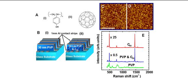
Figure 1. (A) The structure of (i) poly-vinyl-phenol (Sigma Aldrich, purity = 99.9%) and (ii) fullerene (C60) (Sigma Aldrich,
purity = 99.9%) molecules. (B) Schematic diagram of (i) pure PVP metal–organic–metal (MOM) device with macroscopic cross point architecture and (ii) schematic diagram of PVP + C60 devices. (C) Atomic force microscopy (AFM) images of PVP polymer and (D) PVP + C60 blend layer surfaces. (E) Raman spectra of PVP, pure C60 and PVP + C60 blend thin films on quartz substrate. The tangential mode peak of the C60 molecules is clearly present in the blend films and is absent in pure PVP, indicating that they have been incorporated into the material.
in devices consisting of an organic insulator (poly-vinyl- phenol, PVP) and C60 molecules, which could offer significant advantages over existing non-volatile devices. The devices are processed using a solution based technique where the polymer and the fullerenes are dissolved in solvents, creating a uniform blend. A recent paper in Organic Electronics by Majumdar et al describes a similar device with the use of polystyrene and C60 molecules [16].
2. Experimental details
All devices were fabricated by first thermally evaporating (in 1 × 10⁻⁶ Torr vacuum) the Al bottom contact electrodes (300 nm thick and 1 mm wide) onto a clean 2.5 cm × 2.5 cm glass substrate, then spin coating the organic layers (thickness = 30 nm, 7000 RPM). The top Al electrodes were then evaporated in a perpendicular direction to the bottom electrodes, completing the cross point architecture. The PVP polymer solution ratio consisted of 10 g of poly-vinyl-phenol dissolved in 1 l of isopropanol. The mass ratio of PVP polymer to C60 was 10 mg to 0.5 mg. The C60 powder was initially dissolved in toluene and vigorously ultrasonicated in a bath, then added to the polymer/isopropanol solution. The combined blend solution was then ultrasonicated for an additional two hours to ensure that the solution was homogeneous. The thickness of the organic films, kept constant at 30 nm, was measured directly using a high resolution field emission scanning electron microscope (FESEM). After deposition of thin films, the devices were left to dry for 24 h in a desiccator before the top Al electrodes were evaporated. A Digital Instruments Nanoscope atomic force microscope (AFM) in tapping mode at a frequency of 0.3 kHz was used to obtain the images. The root mean square roughness extracted from AFM of the pure PVP and blend layers was 3–5 nm. A Renishaw Raman system 1000 instrument with a Peltier cooled CCD was used to obtain the Raman spectra. The Raman
measurements were carried out with a 785 nm laser with a 2 µm spatial resolution. The I –V characteristics were measured using an Agilent 4156C semiconductor analyser at room temperature with a sweep rate of 10 ms V−1. Electrical delay time measurements were obtained using an Agilent oscilloscope (Agilent 54622A 100 MHz) and a 2020 Data Precision Arbitrary Function Generator. A voltage pulse was applied using one unit and the voltage across a resistor was measured by the other unit to obtain the current delay time.
3. Results and discussion
The chemical structures of the PVP polymer and the C60 fullerene molecule are shown in figure 1(A) ((i) and (ii)). The PVP polymer is insulating and easily dissolves in isopropyl alcohol. The fullerene is a closed cage molecule with a precise diameter (0.72 nm), consisting of 60 carbon atoms, and is easily dissolvable in toluene. A uniform solution of PVP and C60 (5 wt% of C60) is synthesized and spin coated onto patterned Al electrode strips (bottom contacts). The sandwich structures are completed by depositing Al electrode strips on top of the organic layer. The top electrode strips are perpendicular to the bottom electrodes, giving the desired cross point architecture memory devices as shown in figure 1(B) ((i) and (ii)). The spin coated organic films are well adhered, stable and smooth, with an average roughness ranging from 3 to 5 nm as determined by an AFM. Pure PVP or the blend films do not show any surface texture and appear uniform and flat throughout as shown in figures 1 (C) and (D). Also, no pin holes or large aggregates of C60 were detected in our devices, indicating that the blend is homogeneous. The definite incorporation of C60 in our blend films was confirmed by monitoring the A1g tangential Raman mode for C60 near 1469 cm−1 (figure 1(E)). The pure PVP contains small peaks at low wavenumbers but the 1469 cm−1 tangential mode peak is absent while the blend material exhibits a combination of PVP
146

Memory effect in thin films of insulating polymer and C60 nanocomposites
Figure 2. Current versus voltage characteristics of pure PVP and PVP containing C60 devices on glass substrates. (A) The pure PVP MOM devices exhibit negligible hysteresis as the voltage is swept from negative to positive at varying sweep rate. (B) In contrast, the PVP + C60 devices exhibit a distinct hysteresis with a current difference of approximately 50–75 nA between the high and low conduction states. The arrows indicate the direction of the sweep. (C) Conducting AFM measurements on pure PVP (i) and PVP + C60 blend ((i), (ii), (iii), (iv)) devices. Hysteresis is clearly observed, even at this nanoscale, in the blend devices and is absent in the pure PVP device. (D) Schematic of 100 nm × 100 nm square over which the c-AFM measurements were taken.
and C60 peaks. The Raman spectrum of pure C60 thin films is also shown in figure 1(E), for comparison. The uniformity of the C60 distribution was verified by taking a Raman map of the sample surface. Further observations with FESEM and transmission electron microscopy (TEM) did not reveal any inhomogeneities such as segregation or thickness variation.
Typical current–voltage (I –V ) measurements at several sweep voltages of macroscopic (mm2) single-layer Al/PVP/Al and Al/PVP + C60/Al metal–organic–metal (MOM) structures exhibit symmetrical characteristics for negative and positive applied voltages (see figures 2(A) and (B)) and different contact areas (not shown), typical of bulk-limited transport. The PVP only MOM devices show negligible hysteresis (figure 2(A)) while a clear hysteresis can be seen in the PVP + C60 devices (figure 2(B)) at all sweep rates, indicating that C60 is responsible for the hysteresis. It should also be mentioned that devices fabricated from pure C60 thin films deposited by solution and thermal evaporation deposition could not be measured. The fact that the I –V measurements as a function of the sweep rate for the PVP + C60 devices do not show a significant variation in the hysteresis for the sweep times available to us strongly indicates that the effect is real and not an artifact. The hysteresis in our devices is similar to the one reported for organic–metal–organic systems with the exception that the current in our case is higher as the voltage
is swept up and lower as the voltage is decreased [9–14]. Although no clear threshold voltage is observed, the hysteresis in our PVP + C60 devices is sufficiently large, with the maximum difference between the current levels being approximately 50– 75 nA at +1.0 V, which is discernable enough to allow definitive write, read and erase states (see below). The lack of threshold in our devices in comparison to those reported in [9–14] is attributed to the steady shielding of applied bias due to charging of C60 molecules with increasing voltage in our devices. It also points to a dramatically different mechanism responsible for the memory effect. A short circuit current at 0 V is clearly observed in the I –V characteristics of the PVP + C60 devices, as shown in figure 2(B). This is related to the fact that application of the initial negative voltage leads to the injection of electrons into the C60 molecules, which begin to screen the applied voltage. The actual voltage across the device will be different from the applied voltage. This is highlighted by the fact that at 0 V finite current can be measured. Zero current is in fact measured at +1.3 and −1.3 V in the downward and upward sweeps, respectively. These voltages are consistent with our threshold voltage in the C–V measurements, which indicates the voltage induced due to the storage of charge.
Furthermore, in order to investigate the memory effect at the nanoscale, we have used a conducting AFM (c-AFM) to obtain I –V characteristics from nanosized ( 50 nm2)
147
S Paul et al
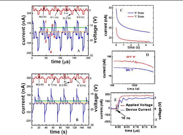
Figure 3. (A) Current versus voltage response of our memory devices during high frequency write–read–erase–read voltage cycles. Initially a voltage pulse of +2.5 V is used for writing (W), which can be read (R) by applying +1 V (‘1’ bit, low conductance). This information can be erased (E) by applying a voltage pulse of −2.5 V. The fact that the original data have been erased can be confirmed by applying +1 V to read (‘0’ bit, high conductance). The ON and OFF states can be clearly distinguished by the large current difference indicated by the two horizontal lines. An argument could be raised that the response of the device could be the result of a simple RC circuit operating with pulses comparable to its RC time constant. However, a simple calculation shows that the time constant would be approximately 80 ms, orders of magnitude higher than the 5 µs pulse widths. (B) Current versus voltage response of our memory devices during low frequency write–read–erase–read voltage cycles. (C). Current decay during reading operation for both ‘0’ and ‘1’ states. The two states remain distinguishable. (D) Data retention graph showing a consistently higher current value for the OFF state than for the ON state. A −2.5 V pulse was applied initially to erase all the data. The ON state (‘1’ bit) was obtained by applying a pulse of +2.5 V and then bringing the voltage down to +1 V, where it was held for 2 h and the current monitored. The OFF state (‘0’ bit) was obtained by applying a −2.5 V pulse and then bringing the voltage up to +1 V, where it was held for 2 h and the current monitored. (E) The plot shows a response time of 10 ns for our devices.
regions in pure PVP and PVP + C60 devices. The c-AFM I –V results shown in figure 2(C) clearly demonstrate that although the current is significantly diminished for nanodevices the hysteresis is preserved at the nanoscale in the blend devices and is absent in the pure PVP devices. Specifically, four I –V characteristics made at four locations spaced 100 nm apart in a square array (see the schematic diagram shown in figure 2(D)) are plotted in figure 2(C) ((i)–(iv)). These results indicate that it will be possible to fabricate nanosized crosspoint memory device arrays using our PVP + C60 blend. We note that the current values do not scale with the electrode area in macroscopic and nanodevices. In order to verify our c-AFM results, we fabricated lithographically patterned gap cell electrodes with a spacing of 30 nm (not shown). Nanodevices were fabricated using pure PVP and PVP + C60 films by drop casting. The pure PVP films did not show a hysteresis, while the PVP + C60 films showed a hysteresis
with current values comparable to the c-AFM data. The lack of scaling is attributed to field enhanced conduction due to Fowler–Nordheim tunnelling in the nanoscale measurements and will be discussed in detail in a future publication.
In order to translate the I –V hysteresis into memory operations, we have measured the read–write–erase cycles of our MOM devices at high (figure 3(A)) and low frequencies (figure 3(B)) using an arbitrary wavefunction generator. It can be seen at point 1 in figure 3(A) and in figure 3(B) that the devices can be tuned from high (‘0’ ON state) to low (‘1’ OFF state) conductivity states by applying +2.5 V (lower voltage than Flash memory devices [17, 18]) to negatively charge the C60 molecules, this could be registered as the ‘write’ step. The write step corresponds to point 1 of the hysteresis loop in figure 2(B). Next, the device is brought down to 0 V, corresponding to point 2 in the hysteresis loop. Then by applying +1.0 V a low current can be recorded (read step)
148

Memory effect in thin films of insulating polymer and C60 nanocomposites
to register a ‘1’ state, as in point 3 in the loop. Next the device is brought back to point 2. The device can now be fully erased by applying −2.5 V to return it to its original OFF state, corresponding to point 4 in the hysteresis loop. The state is next moved to position 5 in the hysteresis loop by applying 0 V. The OFF state is now read by applying a +1.0 V pulse, corresponding to point 6 on the hysteresis loop, providing a higher current than the ON state. Finally, the device is brought back to point 5 with a 0 V pulse. The noticeable decrease in the current during the operation in both the high and low frequency measurements is attributed to a decrease in the effective applied voltage due to screening from charge injection into the blend layer. The high frequency measurements of figure 3(A) show a persistent offset in the current at 0 V. This is because the device does not reach equilibrium during high frequency pulsing, in contrast to the low frequency operation shown in figure 3(B). Figure 3(C) shows that the device takes 1 to 2 s before reaching equilibrium, with a consistent difference in current for both the ‘0’ and ‘1’ states. Thus for any set frequency of operation the ‘0’ and ‘1’ states will remain distinguishable, an important point since memory devices operate at a single frequency. Therefore, during the high frequency operations used in memory technologies today, the offset zero-voltage current would not be a factor in the device performance since the two states would remain distinguishable at the end of the short read operation.
The time-traces in figures 3(A) and (B) could be interpreted as those from a simple RC circuit driven by an asymmetric pulse sequence with pulse widths comparable to the RC time. However, this is not the case in our devices because our calculations reveal a time constant of approximately 80 ms, which is significantly different from the high and low frequency measurements shown in figures 3(A) and (B). Therefore the measured features in figure 3 cannot be completely due to RC effects. The energy dissipation in our memory devices is estimated to be about 0.2 µW for write and erase steps and 60 nW for the read step per bit. The robustness of our MOM devices was tested by monitoring both ON and OFF state currents under continuous voltage as a function of time (see figure 3(D)). No deterioration of the performance was observed for up to 1 h, then a slight decline in both ON and OFF state currents was observed for the next 1 h. However, the difference between the ON and OFF states always remained constant, indicating data retention. It should be remembered that continuous two hour testing of the ON and OFF states translates into a substantially long time since a single read–write–erase cycle is only a few tens of nanoseconds. In addition, we tested the devices up to six months after their fabrication and found that it is possible to carry out read–write–erase operations. The response time of the MOM structure was measured and found to be 10 ns (see figure 3(E)), close to the limit of our measurement apparatus when taking inductance from the circuitry into account. The delay time in nanoseconds suggests that the information access time of these devices is close to DRAM devices.
In order to confirm that the charge injection and retention is indeed occurring in the C60 molecules and not in the polymer, we have carried out capacitance versus voltage (C– V ) and Raman spectroscopy measurements. We discuss the
C–V measurements first. The leakage current in PVP devices is sufficiently low (less than 50 pA), making them suitable for C–V analysis. The C–V data for the two different device structures investigated are shown in figures 4(A) and (B). The C–V curves for the control Al/PVP/SiO2/Si (metal/insulator/semiconductor, MIS) sample (i.e. figure 4(A)) shows the usual accumulation/depletion/inversion characteristics associated with MIS structures. The absolute value of the accumulation capacitance value (≈290 pF) is consistent with that estimated from the PVP film (thickness = 65 nm) on top of the 2 nm SiO2 layer. The C–V measurements on MIS structures containing C60 show significant hysteresis, suggesting charge storage in the C60 layer (figure 4(B)). The direction of hysteresis indicates that the charging of C60 takes place from the semiconductor side by electron tunnelling through the thin oxide layer. Our extensive investigations of the C–V behaviour of these devices lead us to conclude that charge injection and retention, giving rise to the hysteresis in the I –V characteristics, occurs in the C60 molecules.
Although the C–V measurements provide indirect evidence of charge injection and retention in C60 molecules, our Raman analysis provides direct evidence of charge transfer in C60 in our devices. Raman has been used widely to obtain information about charge transfer and functionalization in carbon nanostructures [19]. The devices for measuring charge transfer with Raman were fabricated on ITO coated glass. The ITO served as the bottom transparent and conducting electrode so that Raman could be performed on working devices. The sandwich structure was completed as usual with the deposition of 30 nm organic layer and Al electrodes. In order to investigate the charge injection and discharge in C60, we monitored the A1g Raman mode of a device immediately after fabrication and after application of +2.5 and −2.5 V (write and erase steps, respectively). We found that the Raman A1g mode downshifts by a few wavenumbers upon the application of +2.5 V (even after measurements taken up to 24 h later) but appears at the expected 1469 cm−1 peak position after the erase operation, as shown in figure 4(C). The downward shift of the C60 A1g peak is a strong indication that charge injection into C60 occurs after the write operation. The shift in the Raman peak does not imply that all the C60 molecules are charged. The downshift is attributed to the stimulated transversal vibration of the charged C60 molecules, which is due to the summing of the signals from the charged C60 molecules and uncharged ones. During the write step the number of charged C60 molecules is greater than the neutral molecules and therefore the A1g peak is suppressed and absorbed in the observed downshifted peak. This is similar to other material systems such as carbon nitride films and carbon nanotubes [19–21]. The appearance of the A1g peak at 1469 cm−1 after the erase operation also indicates that the injected charge has been discharged. Thus our C–V and Raman analysis provide strong evidence that C60 molecules are responsible for the hysteresis (and thus the memory effect) in our devices.
The presence of finite current at 0 V raises the question of whether the memory effect is due to the capacitive nature of the device, which would render it volatile. However, the data collected suggest that this is not the case. If the devices acted like capacitors then the change in current during a constant read voltage pulse (see figure 3(C)) would increase
149

S Paul et al
Figure 4. The quasi-static C –V measurements were made on metal–insulator–semiconductor (MIS) structures consisting of an Ohmic bottom Al contact, p-type Si with a 1–2 nm SiO2 layer, organic layer (thickness = 60 nm to prevent leakage current) and top Al electrodes as shown in the insets. (A) The pure PVP device does not show any hysteresis while the (B) MIS device with PVP + C60 shows a hysteresis with a threshold voltage of 1.3 V, indicating that charge storage occurs in the C60 molecules. (C) Raman spectra near the A1g C60 peak of a device after three memory operations. The as-fabricated device shows the C60 A1g mode at the expected 1469 cm−1 peak position (indicated by the vertical line), which shifts downward after the application of 2.5 V pulse (write step), indicating that charge injection into C60 molecules has occurred. The discharging of carriers from the C60 after the application of −2.5 V (erase operation) is clearly indicated by the fact that the A1g appears at the expected 1469 cm−1 peak position.
and the difference in the ‘0’ and ‘1’ states would approach zero after the calculated time constant of 80 ms. Instead, we observe a decrease until 1–2 s, after which the device reaches equilibrium. In addition, the current for both ‘0’ and ‘1’ states remains clearly visible throughout the measured time. The low frequency read–write–erase cycles of figure 3(B) show that after writing or erasing and then waiting for 4 s a ‘1’ or ‘0’ state can be distinguished, indicating that the observed hysteresis in figure 2(B) is not due to slow kinetics that are typically found in electrolytic capacitors. The ON–OFF ratio in figure 3(D) also supports the fact that the devices are not relying on capacitance effects to store the information since the devices continue to maintain a current difference up to an hour. After one hour both current states decay due to degradation of the polymer from continuous operations. In addition, both the C–V and Raman data show that the C60 molecules are charged and maintain their charge up to 24 h, all of which indicate that our devices are non-volatile.
4. Conclusions
In brief, we have demonstrated a memory effect in the form of high and low conduction states in PVP + C60 devices. The use of C60 molecules as the charge storage medium and the ability to disperse them uniformly in an insulating polymer matrix using a solution based technique is promising for high storage density, large area devices. Memory operation at high and low frequencies has been demonstrated and reveals that read–write–erase operations are possible. Conducting AFM
analysis also indicates that the memory effect persists at the nanoscale. The Raman and C–V measurements also indicate that C60 molecules store the charge.
References
[1]Chen J, Reed M A, Rawlett A M and Tour J M 1999 Large on–off ratios and negative differential resistance in a molecular electronic device Science 286 1550–2
[2]Collier C P, Wong E W, Belohradsky M, Raymo F M, Stoddart J F, Kuekes P J, Williams R S and Heath J R 1999 Electronically configurable molecular-based logic gates
Science 285 391–4
[3]Reed M A, Chen J, Rawlett A M, Price D W and
Tour J M 2001 Molecular random access memory cell Appl. Phys. Lett. 78 3735–7
[4]Forrest S R 2004 The path to ubiquitous and low-cost organic electronic appliances on plastic Nature 428 911–8
[5]Gelinck G H, Genus T C and Leeuw D M D 2000 High performance of all-polymer integrated circuits Appl. Phys. Lett. 77 1487–9
[6]Peumans P, Yakimov A and Forrest S R 2003 Small molecular weight organic thin-film photodetectors and solar cells
J. Appl. Phys. 93 3693–723
[7]Ho P K H, Kim J S, Burroughes J H, Becker H, Li S F Y, Brown T M, Cacialli F and Friend R H 2000 Molecular-scale interface engineering for polymer light-emitting diodes Nature 404 481–4
[8]Scott J C 2004 Is there an immortal memory? Science
304 62–3
[9]Ma D, Aguiar M, Freire J A and Hummelgen I A 2000 Organic reversible switching devices for memory applications Adv. Mater. 12 1063–6
150

Memory effect in thin films of insulating polymer and C60 nanocomposites
[10]Ma L P, Liu J and Yang Y 2002 Organic electrical bistable devices and rewrittable memory cells Appl. Phys. Lett. 80 2997–9
[11]Ma L P, Pyo S, Ouyang J, Xu Q F and Yang Y 2003 Nonvolatile electrical bistability of organic/metal–nanocluster/organic system Appl. Phys. Lett. 82 1419–21
[12]Bozano L D, Kean B W, Deline V R, Salem J R and
Scott J C 2004 Mechanism for bistability in organic memory elements Appl. Phys. Lett. 84 607–9
[13] Moller¨ S, Perlov C, Jackson W, Taussig C and
Forrest S R 2003 A polymer/semiconductor write-once read-many-times memory Nature 426 166–9
[14]Chu C-W, Ouyang J, Tseng J-H and Yang Y 2005 Organic donor–acceptor system exhibiting electrical bistability for use in memory devices Adv. Mater. 17 1440–3
[15]Ouyang J, Chu C-W, Szmanda C R, Ma L and Yang Y 2004 Programmable polymer thin film and non-volatile memory device Nat. Mater. 3 918–22
¨
[16] Majumdar H S, Baral J K, Osterbacka R, Ikkala O and Stubb H 2005 Fullerene-based bistable devices and associated negative differential resistance effect Org. Electron. 6 188–92
[17] Paul S, Pearson C, Molloy A, Cousins M A, Green M, Kolliopoulou S, Dimitrakis P, Normad P, Tsoukalas D and Petty M C 2003 Langmuir–Blodgett film deposition of metallic nanoparticles and their application to electronic memory structures Nano Lett. 3 533–6
[18] Bez R, Camerlenghi E, Modelli A and Visconti A 2003 Introduction to flash memory IEEE Proc. 91 489–502
[19] Haddon R C et al 1991 Conducting films of C60 and C70 by alkali-metal doping Nature 350 320–2
[20] Fanchini G, Tagliaferro A, Messina G, Santangelo S,
Paoletti A and Tucciaron A 2002 Vibrational properties and microstructure of reactively sputtered hydrogenated carbon nitrides’ J. Appl. Phys. 91 1155–65
[21] Martin T P and Genzel L 1973 Raman scattering in small crystals Phys. Rev. B 8 1630–5
151