

nanotechnology / nano6_4_015
.pdfINSTITUTE OF PHYSICS PUBLISHING |
NANOTECHNOLOGY |
Nanotechnology 17 (2006) 927–932 |
doi:10.1088/0957-4484/17/4/015 |
A hybrid mask–mould lithography scheme and its application in nanoscale organic thin film transistors
Xing Cheng1, Dawen Li and L Jay Guo2
Solid-State Electronics Laboratory, Department of Electrical Engineering and Computer
Science, University of Michigan, Ann Arbor, MI 48109-2122, USA
E-mail: guo@umich.edu
Received 6 September 2005, in final form 28 December 2005
Published 30 January 2006
Online at stacks.iop.org/Nano/17/927
Abstract
Nanoimprint lithography (NIL) has stimulated great interest in both academic research and industrial development due to its high resolution, high throughput and low cost advantages. Though NIL has been demonstrated to be very successful in replicating nanoscale features, it also has its limitations as a general lithography technique. Its fundamental moulding characteristics (i.e. physically displacing polymer materials) frequently lead to pattern defects when replicating arbitrary patterns, especially patterns with broad size distribution. To solve this problem, we have developed a combined nanoimprint and photolithography technique that uses a hybrid mould to achieve good pattern definitions. In this work, we applied this technique to fabricate finger-shaped nanoelectrodes, and demonstrated nanoscale pentacene organic thin film transistors (OTFTs). Methods of the hybrid mask–mould (HMM) fabrication and results on the device electrical characteristics are provided. With combined advantages of both photolithography and NIL, and the applicability to general nanoscale device and system fabrication, this method can become a valuable choice for low cost mass production of microand nanoscale structures, devices and systems.
(Some figures in this article are in colour only in the electronic version)
Lithography, a process that defines microand nanoscale patterns on a substrate, is one of the most critical steps in micro-device fabrication. Photolithography and electron beam lithography (EBL) have been the standard techniques for the microelectronic industry for years. As the feature size of the microelectronic devices continues to shrink into the sub-100 nm region, significant amounts of resources and research effort have been poured into the development of the next generation lithography (NGL) systems to accommodate the need of advanced lithographies for future microelectronic fabrication. However, the NGL systems in development, such as 157 nm optical lithography, extreme UV scanners, x- ray lithography and projection electron-beam lithography, are
1Present address: Electrical and Computer Engineering Department, Texas A&M University, College Station, TX 77843-3128, USA.
2Author to whom any correspondence should be addressed.
complicated and costly; there are also many key technical issues (such as light sources, lenses, and mask materials, to name only a few) that need a breakthrough in order to put them into widespread practical use. Though immersion lithography with a 193 nm system shows great potential down to 65 nm [1], it remains very challenging for developing sub65 nm lithography systems for mass industrial fabrication.
At the same time, non-conventional lithography techniques, especially nanoimprint lithography (NIL) [2], have attracted more and more interest due to their excellent capability in nanoscale patterning. NIL uses a physical moulding process to replicate patterns. It can be very high resolution, and only requires simple equipment set-up [3, 4]. It is an easy process that has high throughput, thus enabling low cost large scale patterning of nanostructures. However, it also has some problems that could limit its applications. In NIL it almost always
0957-4484/06/040927+06$30.00 © 2006 IOP Publishing Ltd Printed in the UK |
927 |
X Cheng et al
Figure 1. Schematic diagram of the hybrid mask–mould (HMM).
requires a separate reactive ion etching (RIE) step to remove the residual layer after imprinting. The residual layer removal can be difficult for complex mould patterns because the layer thickness is non-uniform across the substrate after imprinting. During the moulding process of the NIL technique, resist materials displaced by the protrusion patterns on the mould have to be accommodated by the empty areas on the mould, thus the mould pattern complexity can lead to imprinting defects [5–9]. It is especially problematic when both large scale (tens of microns and larger) and nanoscale patterns coexist on the mould and in close proximity. For step and flash imprint lithography (SFIL), this problem is alleviated by using low viscosity liquid resist [10]. Though patterns as large as 20 µm and as small as 40 nm have been successfully replicated at the same time by SFIL [11], this technique may still encounter defects or non-uniform residual layer thickness for structures of hundreds of microns due to its very low imprinting pressure ( 0.25 psi). Most device applications require arbitrary combinations of large and small patterns. This reality can greatly limit the application of the NIL for certain device fabrications. Therefore more development is required in order to expand the application of the NIL in the fabrication of general microand nanodevices and systems.
To overcome its difficulty in patterning arbitrary patterns, we have come up with a new scheme to lift this limitation. The hybrid-mask–mould (HMM) scheme is a modified NIL technique that intimately combines the conventional photolithography and NIL together. With such combination, we can exploit the strength of each technique to circumvent their limitations, and can replicate patterns of arbitrary sizes in one lithography step. We have previously demonstrated patterning both large structure and sub-micron structure in one lithography step by using this technique [12]. In this work, the HMM scheme is expanded as a general lithography technique for device fabrication. It is employed to fabricate organic thinfilm transistors (OTFTs) with sub-100 nm finger electrodes. The fabrication of the HMM, the pattern replication with the HMM and the performance of the OTFT fabricated by the HMM scheme are discussed in detail.
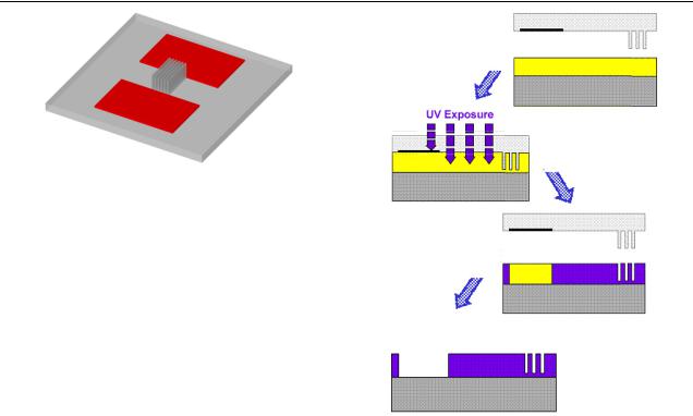
A schematic diagram of the HMM is shown in figure 1. The HMM is made of UV transparent material such as fused silica. Nanoscale protrusions on the mould will be used to replicate nanoscale patterns through NIL. Large size metal pads are also placed on the HMM to serve as a light mask for patterning a large structure as in conventional photolithography. In other words, the HMM simultaneously serves as an NIL mould and a photomask. The replication steps
(a)
(b)
(c)
After Developing
(d)
Figure 2. Schematic diagram of pattern replication with HMM. (a) NIL with HMM on SU-8 resist; (b) flood UV exposure after imprinting; (c) mould–substrate separation; (d) developing to remove unexposed resist. Both large and nanoscale patterns are obtained after developing.
with the HMM are shown in figure 2 with the use of a negative tone photoresist, such as SU-8. After spin-coating the resist, the HMM and the substrate are brought together (figure 2(a)). Heat and pressure are then applied to the assembly. The nanoscale protrusions on the HMM are pressed into the resist layer. After imprinting, a flood UV exposure through the UV transparent HMM creates the latent images of the metal patterns in the resist (figure 2(b)), because the resist underneath the large metal pads will not be exposed. The HMM and the substrate are then separated (figure 2(c)). The nanoscale patterns are already formed at this step by NIL. The unexposed negative tone resist underneath the metal pads can be easily removed by using a developer, completing the definition of large patterns (figure 2(d)). With this single lithography step, patterns of arbitrary sizes can be easily replicated with very low cost.
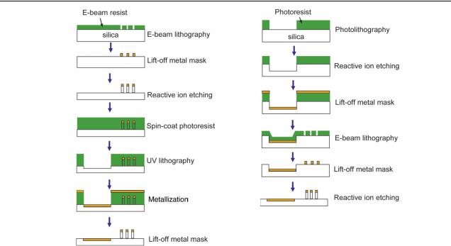
The fabrication of the HMM is pivotal in this new lithography technique. As in the fabrication of the conventional NIL mould, the HMM can be fabricated by standard microelectronic fabrication processes such as lithography, reactive ion etching (RIE) and metallization. To create the patterns on the mould, both photolithography and EBL are required. Photolithography is used to define the large patterns (the metal pads) while EBL is used to define the nanoscale patterns (the nanoscale protrusions) on the HMM. Depending on the sequence of the lithography steps, two HMM fabrication schemes can be used, as shown in figure 3. In the first scheme (figure 3(a)), the nanoscale structure is
928
A hybrid mask–mould lithography scheme and its application in nanoscale organic thin film transistors
(a) |
(b) |
Figure 3. Methods of HMM fabrication. (a) EBL followed by photolithography scheme; (b) photolithography followed by EBL scheme.
first defined by EBL, followed by metallization and RIE of the silica substrate. Then the large metal pads are added onto the mould by conventional contact photolithography and metallization. In the second scheme (figure 3(b)), the sequence of the lithography steps is reversed. Photolithography is employed first to place the large metal pads on the silica substrate, then EBL and RIE are used to create the nanoscale protrusions to complete the fabrication of the HMM. It should be noted that the second scheme has an advantage over the first scheme in terms of pattern placement. EBL has better pattern placement accuracy than photolithography. Thus the second scheme, where photolithography is followed by EBL, allows accurate placement of nanoscale patterns with respect to the large structures. This is especially crucial for devices in which precise control of nanoscale pattern position is required. We provide next detailed processing steps for making an HMM used for the fabrication of nanoscale organic thin film transistors.
The HMM for OTFT fabrication contains finger electrodes separated by a nanoscale gap ( 50 nm) for source and drain connection and large metal pads ( 150 µm) for probing during electrical characterization of the device. To fabricate the HMM, we use the second scheme (figure 3(b)), where photolithography is followed by EBL because of the aforementioned advantage. On a silica substrate, photoresist 1813 is spin-coated and soft-baked on a hotplate to drive out solvents. Then the large metal pad pattern is defined by a contact aligner (MJB-3) through a photomask. After developing the photoresist, the silica substrate is dry-etched by CHF3 chemistry using the photoresist as the etching mask. A titanium/nickel bilayer (5/70 nm) is evaporated onto the substrate. After lift-off in acetone, 100 nm thick 950 000 molecular weight (Mw) poly(methyl methacrylate) (PMMA) is spin-coated on the substrate for EBL. Because the
substrate is non-conductive, a 20 nm thick aluminium layer is evaporated on the top of the PMMA resist for discharging during EBL to achieve high resolution patterns. The EBL is carried out in a Raith 150 tool. After EBL, the thin aluminium layer is first removed in ammonium hydroxide solution, and then the PMMA is developed in MIBK and IPA mixture (1:3 ratio). A titanium/nickel bilayer (5/25 nm) is evaporated on the silica substrate. After lift-off, the nanoscale protrusions are formed by dry etching using CHF3 chemistry. The fabricated HMM is then vapour-coated with surfactant perfluorodecyltrichlorosilane to facilitate mould release during the replication process [13].
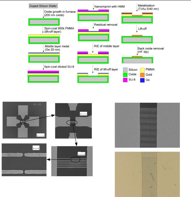
The fabrication of the nanoelectrodes for the nanoscale OTFTs with the HMM is outlined in figure 4. Starting from a highly doped n-type silicon substrate (resistivity 0.001–0.004 cm) serving as the bottom gate electrode, a 200 nm thick thermal oxide grown on the substrate serves as a gate dielectric. To pattern the source and the drain nanoelectrodes, we use tri-layer resist to ensure good lift-off results [14, 15]. The tri-layer resist consists of a 100 nm thick 950 000 Mw PMMA on the Si/SiO2 substrate formed by spin-coating, a 20 nm thick germanium layer deposited by thermal evaporation, and a thin layer of negative tone resist SU-8 ( 120 nm thick) that is spin-coated on the top of the germanium layer from diluted SU-8 solution in propylene glycol monomethyl ether acetate (PGMEA). Nanoelectrodes and large contact pads are formed in the SU-8 layer by onestep lithography using the fabricated HMM. The imprinting is done at 80 ◦C and 4.3 × 10⁶ Pa for 5 min. After imprinting and before separating the mould–substrate assembly, the SU- 8 resist is exposed by 365 nm UV light through the HMM with a fluence of 80 mJ cm−2. After separating the substrate from the HMM, the unexposed SU-8 is removed by soaking the substrate in PGMEA solution for 1 min followed by 1 min
929
X Cheng et al
Figure 4. Schematic diagram of nanoelectrode replication steps with HMM and tri-layer resist.
(a)
10 m
100 m
200 nm
2 |
m |
(b) |
Figure 5. SEM micrographs of a finger-shaped nanoelectrode achieved along with large metal pads by the one-step lithography process outlined in figure 4.
rinse in IPA. Then, the residual layer after NIL is removed with a few seconds of oxygen RIE to expose the germanium layer. The middle germanium layer is then dry etched with CHF3 RIE. Then, the PMMA bottom layer is dry etched with oxygen RIE using the germanium layer as an etching mask. A slight over-etch of the PMMA layer creates an undercut feature which facilitates the lift-off process. Finally, a titanium/gold bilayer (5/40 nm) is evaporated onto the substrate and lifted off in acetone to form the nanoelectrode structure. Figure 5 shows SEM micrographs of nanoelectrodes connected to large metal contact pads. Finger shaped nanoelectrodes of around 100 nm width separated by around 50 nm gap along with the large 150 µm contact pads are achieved by this one-step lithography technique.
Pentacene OTFTs with bottom contact configuration are fabricated using the above electrode structure. A 40 nm thick pentacene thin film is thermally evaporated on the top of
Figure 6. (a) SEM micrograph of finger-shaped nanoelectrodes and
(b) optical micrograph of OTFT.
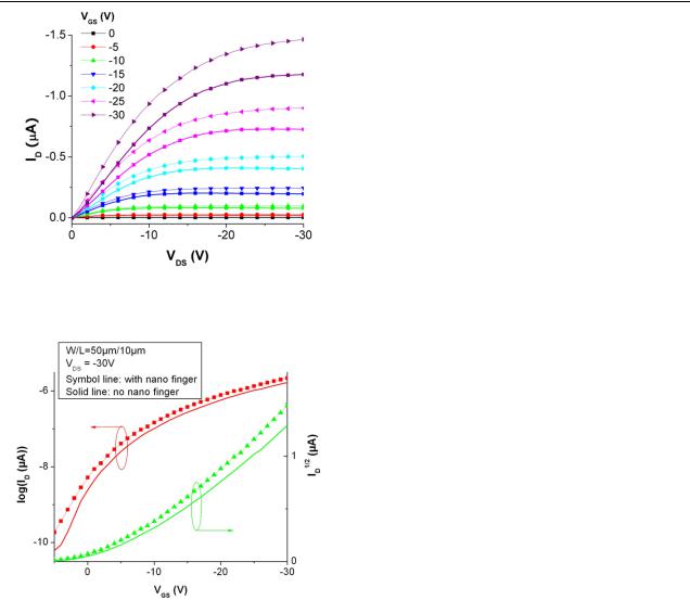
the electrodes in a high vacuum. Figure 6 shows an optical micrograph of the OTFT device with pentacene on top of the nanoelectrode, along with an SEM micrograph of the same nanoelectrode. Device measurement and characterization are done immediately after the pentacene evaporation. The output and transfer characteristics of a pentacene OTFT with multiple fingers and 100 nm gap (W /L = 30) are shown in figures 7 and 8, respectively. Figures 7 and 8 also show the characteristics of a pentacene OTFT without finger nanoelectrodes (W = 50 µm, L = 10 µm). Compared with the micron scale pentacene OTFT (W /L = 5), the OTFTs with nanoelectrodes inside the micron channel did not exhibit significant increase in device performance, though the W /L
930
A hybrid mask–mould lithography scheme and its application in nanoscale organic thin film transistors
Figure 7. ID versus VD characteristics of pentacene OTFT.
Figure 8. Transfer characteristics of pentacene OTFT.
ratio is increased to 30 for the nanoelectrode OTFT due to the reduction of the channel length by the nanoscale gap. The less significant increase of drain current for pentacene OTFTs with nanoelectrodes originates from the effect of contact resistance on OTFTs. When the channel length of bottom contact pentacene OTFTs becomes smaller (less than 10 µm), the contact resistance dominates the total resistance (including both contact resistance and channel resistance) [16]. It has been found that the grain size of the pentacene deposited on the gold surface is much smaller than that on the oxide surface [17]. These small grains at the gold/pentacene interface result in much larger contact resistance than short channel resistance. The further shrinking down of the channel length to nanoscale does not effectively increase the drain current. The extracted field-effect mobility for the nanoscale pentacene OTFTs from the transfer characteristics in the saturation regime is 1.59 × 10⁻² cm2 V−1 s−1, which is similar to other reported values for nanoscale pentacene OTFTs [18].
In summary, we have demonstrated the application of the HMM lithography technique in one-step fabrication of
nanoelectrodes for pentacene OTFTs. This serves as an example to show that the HMM scheme can be applied in general nanoscale device and system fabrications. In most nanoscale devices and systems, it is typical to have both large and nanoscale structures for different functions. Neither conventional photolithography nor NIL alone can satisfy the fabrication needs. The HMM scheme holds great promise to solve this dilemma with broad application scope. This method should also work well with UV-curable liquid resists that are often favoured as the ideal NIL and SFIL resists for room temperature and low pressure processing [19]. Since this method maintains the advantages of high throughput of both photolithography and NIL, it is particularly attractive for low cost industrial mass fabrication.
References
[1] Owa S, Nagasaka H, Ishii Y, Hirakawa O and
Yamamoto T 2004 Feasibility of immersion lithography Optical Microlithography vol XVII (Santa Clara, CA: SPIE)
[2]Chou S Y, Krauss P R and Renstrom P J 1995 Imprint of sub-25 nm vias and trenches in polymers Appl. Phys. Lett. 67 3114–6
[3]Chou S Y, Krauss P R and Renstrom P J 1996 Imprint lithography with 25-nanometer resolution Science 272 85–7
[4]Chou S Y, Krauss P R, Zhang W, Guo L and Zhuang L 1997 Sub-10 nm inprint lithography and applications J. Vac. Sci. Technol. B 15 2897–904
[5]Heyderman L J, Schift H, David C, Gobrecht J and
Schweizer T 2000 Flow behaviour of thin polymer films used for hot embossing lithography Microelectron. Eng.
54229–45
[6]Otto M, Bender M, Hadam B, Spangenberg B and Kurz H 2001 Characterization and application of a UV-based imprint technique Microelectron. Eng. 57/58 361–6
[7]Scheer H-C and Schulz H 2001 A contribution to the flow behaviour of thin polymer films during hot embossing lithography Microelectron. Eng. 56 311–32
[8]Scheer H-C, Schulz H, Hoffmann T and Sotomayor
Torres C M 1998 Problems of the nanoimprinting technique for nanometer scale pattern definition J. Vac. Sci. Technol. B
163917–21
[9]Schift H, Heyderman L J, Auf der Maur M and
Gobrecht J 2001 Pattern formation in hot embossing of thin polymer films Nanotechnology 12 173–7
[10]Stewart M D, Johnson S C, Sreenivasan S V, Resnick D J and Willson C G 2005 Nanofabrication with step and flash imprint lithography J. Microlith. Microfab. Microsyst.
4 011002–6
[11]McMackin I, Choi J, Schumaker P, Nguyen V, Xu F, Thompson E, Babbs D, Sreenivasan S V, Watts M and Schumaker N 2004 Step and repeat UV nanoimprint lithography tools and processes Emerging Lithographic Technologies vol VIII (Santa Clara, CA: SPIE)
[12]Cheng X, Chang M-H and Guo L J 2004 Combined nanoimprint and photolithography technique with a hybrid mold Emerging Lithographic Technologies vol VIII (Santa Clara, CA: SPIE)
[13]Beck M, Graczyk M, Maximov I, Sarwe E-L, Ling T G I, Keil M and Montelius L 2002 Improving stamps for 10 nm level wafer scale nanoimprint lithography Microelectron. Eng. 61/62 441–8
[14]Chen Y, Lebib A, Li S, Pepin A, Peyrade D, Natali M and Cambril E 2000 Nanoimprint and micro-contact printing tri-layer processes Eur. Phys. 12 223–9
[15]Lebib A, Chen Y, Carcenac F, Cambril E, Manin L,
Couraud L and Launois H 2000 Tri-layer systems for
931

X Cheng et al
nanoimprint lithography with an improved process latitude
Microelectron. Eng. 53 175–8
[16]Li D and Guo L J 2006 Micron-scale organic thin film transistors with PEDOT electrodes patterned by polymer inking Appl. Phys. Lett. 88 at press
[17]Dimitrakopoulos D and Malenfant R L 2002 Organic thin film transistors for large area electronics Adv. Mater. 14 99–117
[18]Zhang Y, Petta J R, Ambily S, Shen Y, Ralph D C and Malliaras G G 2003 30 nm channel length pentacene transistors Adv. Mater. 15 1632–5
[19]Cheng X, Guo L J and Fu P-F 2005 Room-temperature, low-pressure nanoimprinting based on cationic photopolymerization of novel epoxysilicone monomers Adv. Mater. 17 1419–24
932