

nanotechnology / t30920.!!!pdf
.pdfINSTITUTE OF PHYSICS PUBLISHING |
NANOTECHNOLOGY |
Nanotechnology 14 (2003) 1043–1050 |
PII: S0957-4484(03)61666-1 |
Electronic transport in monolayers of phthalocyanine polymers
S J Tans1,3, R G Miedema1, L J Geerligs1, C Dekker1, J Wu2,
D Neher2 and G Wegner2
1Department of Applied Physics and DIMES, Delft University of Technology, Lorentzweg 1, 2628 CJ Delft, The Netherlands
2Max-Planck-Institut fur¨ Polymerforschung, PO Box 3148, W-55021 Mainz, Germany
Received 2 April 2003, in final form 9 July 2003
Published 19 August 2003
Online at stacks.iop.org/Nano/14/1043
Abstract
We report on a study of the electrical-transport properties of monolayers of phthalocyaninepolysiloxane (PcPS) polymers, and evaluate their potential for use as molecular wires. Monolayers have been deposited with the Langmuir–Blodgett technique on top of Si/SiO2 substrates with interdigitated electrodes. Current–voltage curves have been measured as a function of temperature for samples with varying electrode distance and number of monolayers. In the undoped state, the conduction is well described by the space-charge-limited-current model. From the data we obtain material characteristics such as the density of trap states within the gap and an estimate of the charge-carrier mobility. It appears that the conductivity is too low to yield a measurable current through a single PcPS polymer. Chemical doping and a field effect have been investigated. Oxygen is effective in doping the PcPS layers, resulting in a two orders of magnitude increase of the conductivity. Iodine is not effective as a dopant. By application of a voltage on a back-gate, we observe a field-effect-induced increase of the conductivity by three orders of magnitude. The effect however decays rapidly in time.
1. Introduction
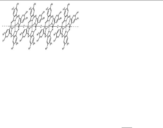
In the past decade there has been considerable progress in the controlled synthesis of rigid-rod conducting molecules [1–5]. One of the motivations for this effort is their possible future employment in electronics on a molecular scale [6]. This requires molecules with very specific qualities. In addition to the conductive properties, a combination of chemical stability, rigidity, length and the possibility of controlled deposition is important. These issues have been addressed in the synthesis of the polymer phthalocyaninepolysiloxane (PcPS; see figure 1) [7, 8]. PcPS is built up from chemically very stable phthalocyanine monomers that are stacked into a rigidrod polymer. Deposition of these macromolecules by means of the Langmuir–Blodgett (LB) technique has become possible by decorating them with flexible alkyl side chains. In previous studies we have described how the controlled LB deposition of the PcPS polymers in monolayers as well as in sub-monolayer
3 Present address: FOM Institute for Atomic and Molecular Physics, Kruislaan 407, 1098 SJ Amsterdam, The Netherlands.
coverage is feasible [9, 10]. Conductivity studies have up till now been performed on bulk samples of phthalocyanine crystals [11]. The stacking of the phthalocyanine monomers in these crystals is similar to that for PcPS. In both cases the monomers are linked together by O atoms that attach to the centre Si atom of the phthalocyanine. The overlap between the π -orbitals of the monomers yields semiconducting properties. It has been shown that in this solid form, the conductivity of the phthalocyanine polymers can be increased by at least five orders of magnitude by various chemical dopants, possibly even attaining a metallic-like state [11]. Because of the favourable combination of structural and electrical properties, the PcPS polymer is an interesting candidate for electricaltransport experiments on individual molecules.
In this paper we first present a study of the in-plane electrical transport in undoped monolayers of PcPS polymers deposited by the LB technique. Single or multiple monolayers of PcPS are deposited on top of electron-beam-defined electrodes with an interdigitated geometry and different electrode spacings. Current–voltage characteristics of these
0957-4484/03/091043+08$30.00 © 2003 IOP Publishing Ltd Printed in the UK |
1043 |
S J Tans et al
Figure 1. Schematic diagram of the polymer PcPS. (R1 = CH3; R2 = ((CH2)7CH3)). Possible twist angles between the monomers are not shown. The polymers have a total diameter of about 2 nm and a length between 20 and 100 nm. The overlap between the
π orbitals of the phthalocyanine monomers renders it a semiconducting material.
samples are measured in vacuum as a function of temperature. The results are well described by the space-charge-limited- current (SCLC) model (see [12] for an overview). This model describes charge injection into a low-conductivity material. In this case, the concentration of injected charge may exceed the intrinsic charge concentration, and space charge builds up in the sample. Fits of this model provide useful material characteristics such as the trap distribution in the semiconducting gap, the position of the Fermi energy and the charge carrier mobility. Finally, we will briefly discuss the effect of oxygen and iodine, which in the Pc bulk studies were shown to be effective dopants. Also, a gate electrode has been used to modulate the conductivity of PcPS layers by a field effect.
2. Space-charge-limited currents
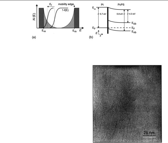
In this paragraph we briefly describe the SCLC theory for our specific sample geometry. In the absence of dopants, a large-bandgap semiconductor will have a low concentration of thermally excited charge carriers and a corresponding low electrical conductivity. In this case, the concentration of injected excess charge carriers can become significant. The amount of this space charge is determined by the applied voltage over the two electrodes and the capacitive coupling between the space charge and compensating charges on the electrodes. At a certain threshold voltage Vx the concentration of injected charge is equal to the concentration of intrinsic charge. For V Vx the current is limited by the space charge [12]. For voltages lower than Vx the intrinsic charge carriers are dominant, which leads to an ohmic current–voltage relation. The specific functional form of the SCLC current versus voltage (I–V ) curve depends on the distribution of charge traps in the bandgap. We adopt the usual assumption of an exponential trap distribution (see figure 2(a)) [12–14]:
|
= |
|
0 |
|
− |
kTc |
|
N(E) |
|
N |
|
exp |
|
E − Evb |
(1) |
|
|
|
|
where N0 is the density of trap states at the valence-band-edge energy Evb. The characteristic width of the exponential trap distribution is set by the energy kTc.
A single analytical expression for the current density which includes both the ohmic and the SCLC regime can then be derived by integration of Poisson’s equation [13, 14]:
J = pµe 1 + |
V |
β V |
, |
|
|
|
|
|
(2) |
||
Vx |
L |
||||
where L is the distance between the electrodes, µ the chargecarrier mobility, p = Nv exp(−(Ef − Evb)/ kT ) is the concentration of thermally activated charge carriers and β = Tc/ T . Nv is the effective density of states in the valence band and Ef the Fermi level. The charge carriers thus are assumed to be thermally excited from the traps to delocalized band states where they contribute to the current. In the pure SCLC regime (V Vx ), equation (2) reduces to a power-law dependence of the current on the bias voltage, and can be written as [13, 14]
J = |
Nv L m |
Vm |
β+1 |
(3) |
||
. |
||||||
|
µeV |
|
V |
|
|
|
Figure 2(a) illustrates the effect of the space charge on the Fermi level in the SCLC regime: upon an increase of the bias voltage, the increased positive space charge will occupy the first available trap states for holes in the bandgap, which corresponds to a shift of Ef towards the band edge. At the bias voltage Vm all the traps are filled and Ef is equal to the bandedge energy Evb. Vm and the corresponding current density Jm at this point is independent of temperature. The SCLC powerlaw asymptotes (equation (3)) for different temperatures thus all intersect at J = Jm, V = Vm, with
Vm = |
eNtot Lt |
(4) |
|
|
, |
||
where Ntot = kTc N0 is the total trap density and t is the thickness of the film covering the electrodes. /t L is a measure for the capacitive coupling between the space charge and the electrodes [15], and therefore a function of the electrode geometry. In contrast to the parallel-plate geometry generally used, the electrodes in our case have a flat interdigitated geometry, which results in a different capacitive coupling. This yields the slightly different expression for Vm, and thus a different functional dependence between the current density and the electrode distance. All equations indicated in this paper apply to an interdigitated geometry. In our case we have J L−(β+1) (cf equation (3)) instead of the common
J L−2(β+1). The current density Jm at V |
= Vm can be |
||
determined by substituting equation (4) in (3): |
|
||
Jm = |
µNveVm |
. |
(5) |
L |
|||
From the intersection point (Vm, Jm) the total trap density Ntot and the value µNv can thus be determined experimentally. We may rewrite equation (2) in the following form:
Evb − Ef = kTc(ln V − ln Vm). |
(6) |
In the SCLC regime Evb − Ef is thus linearly dependent on ln V .
1044
Electronic transport in monolayers of phthalocyanine polymers
Figure 2. (a) Schematic diagram of the proposed density of states as a function of energy (N(E)). Evb and Ecb mark the edges of the valence and the conduction bands respectively. In the bandgap, the exponential distribution of localized states is indicated in grey. The shift of the Fermi distribution for holes 1 − f (E) illustrates the space-charge-limited-current model. Upon application of a high electric field, space charge builds up in the sample, resulting in a shift of the Fermi energy Ef towards the valence band and a corresponding increase in current. (b) Schematic diagram of the polymer–electrode interface.
3. Sample layout and measurement set-up
In PcPS Si-phthalocyanine monomers [7] are linked together through oxygen atoms into 20–100 nm long stacked arrays. The resulting small distance between monomers—the repeat distance is 0.33 nm—leads to π -orbital overlap between monomers and accounts for the mechanical rigidity of PcPS. Including the hydrocarbon side chains, which ensure solubility and the possibility of LB deposition, the total PcPS diameter amounts to 2.4 nm. In our LB method, a monolayer of the flatlying PcPS polymers is formed at the air–water interface in a Langmuir trough because of their form-anisotropic shape [3]. Figure 3 shows a TEM image of a mixed PcPS/cellulose monolayer, which enables a higher contrast of the PcPS molecules. The films used in the conductivity studies presented here are deposited similarly, but are composed of PcPS only. The polymers are oriented with their axis parallel to the substrate and roughly along the dipping direction. Disclinations in the PcPS pattern are observed, however. The PcPS polymers are ordered head to tail [9], which accounts for the large apparent length of the chainlike features in the TEM image.
Interdigitated electrodes were defined by electron-beam lithography on a Si/SiO2 substrate. The electrodes are composed of a 15 nm thick Pt layer on top of a 5 nm thick Ti adhesion layer. The 100 nm wide electrode contacts have a total effective electrode length of 210 µm for all samples. The high work-function of Pt ( 5.7 eV) is of importance for realizing an ohmic electrode–polymer contact. In figure 2(b), a schematic diagram of the polymer–electrode interface is given. Previous studies have shown that PcPS acts as a p-type semiconductor [3]. From UV–vis absorption studies the bandgap of PcPS is determined to be 1.5 eV [3]. The position of the valence band is at 5.8 eV [16]. With a Pt work-function of 5.7 eV we therefore expect an ohmic contact between the PcPS and the Pt electrode. Pt was also chosen for its small grain size (2–5 nm), which allows the fabrication of very thin electrodes. PcPS monolayers are transferred on top of the electrodes and the substrate in a single dip [9]. Atomic force microscopy studies have shown that the LB transfer process is not perturbed by the presence of the corrugated electrodes on the substrate [10]. Samples with one PcPS monolayer as well as nine PcPS layers have been studied. The spacing between the electrodes was either 0.2 or 1 µm.
Figure 3. TEM image of a PcPS monolayer as deposited with the LB technique. This particular film is a mixture of PcPS molecules and cellulose, which separates the PcPS molecules and gives higher contrast in TEM images. The films that we study here are deposited in the same way, but are composed only of PcPS. The PcPS polymers are oriented with their long axes parallel to the surface. The polymers are ordered head to tail, which accounts for their large apparent length.
Measurements are performed in a He flow cryostat with a base temperature of 4 K. The flow cryostat was operated without the usual He heat-exchange gas to enable measurements in vacuum ( 1 mbar). The temperature was regulated with an Oxford temperature controller using a Rh–Fe temperature sensor and a heater mounted on the sample stage. Currents were measured using a Keithley 617 electrometer. Special care was taken in wiring the set-up, which has a leakage resistance of 1 P . The leakage current of a bare sample, that is the electrodes on the substrate without any deposited layer, was determined to be at least two orders of magnitude lower than that for samples with a deposited PcPS layer. Prior to measuring, the samples are degassed for 48 h at room temperature (RT) in the evacuated sample chamber with a pressure of 1 mbar in order to reduce contaminants which may act as unintentional dopants. Current–voltage
1045
S J Tans et al
Figure 4. Current–voltage characteristics of a PcPS monolayer on top of an interdigitated electrodes with spacings of 0.2 µm (a) and 1 µm
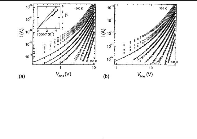
(b) taken at varying temperatures. The curves are taken at regular intervals of 19 K between 135 and 360 K. The solid curves are fits to equation (2), which describes an ohmic current at low voltages and a power-law behaviour for the SCLC regime at high voltages. A leakage conductivity of (5 × 10¹⁶ )−1 was subtracted from the original data. Inset, fit parameter β as a function of the inverse temperature for single monolayer samples with electrode spacings of 0.2 µm (circles) and 1 µm (dots). The fitted straight line through zero indicates an exponential trap distribution. From these fits, Tc is determined to be 1.5 × 10³ and 1.9 × 10³ K respectively.
curves are traces from negative to positive voltage and back at temperatures between 135 and 360 K. With a properly degassed sample, hysteresis of the I–V curves was negligible. Only the up traces are displayed.
For the iodine doping experiments, pristine undoped PcPS layers on top of the electrodes are exposed to iodine vapour. The samples were placed in a glass reactor vessel connected to a second vessel containing the I2 source. Both vessels were thoroughly flushed with Ar gas prior to measuring. After briefly opening the connection between the two vessels, the conductivity of the sample is measured in situ as a function of time.
Table 1. Fit parameters resulting from two different fit procedures based on the SCLC model as described in section 2. The fitted data are that of PcPS monolayer samples with 0.2 and 1.0 µm electrode spacings. The first set of parameters (columns 2–4) results from a fit of equation (2) on the I –V curves that are displayed in figure 4. The second set results from a fit of equation (6) to the data set of figure 8.
|
|
|
|
|
|
|
|
|
Temperature |
|
|
||
|
|
|
I –V curves |
|
|
|
|
dependence |
|
|
|||
|
|
(equation (2)) |
|
|
|
(equation (6)) |
|
|
|||||
Spacing |
|
|
|
|
|
|
|
|
|
|
|
|
|
Jm |
|
Fm |
|
Tc |
|
|
Fm |
|
Tc |
|
|
|
|
(µm) |
(A m−2) |
(V m−1) |
(K) |
(V m−1) |
(K) |
|
|
|
|||||
|
|
5 |
|
8 |
|
3 |
|
8 |
|
× |
3 |
||
0.2 |
2.0 |
× 105 |
1.7 |
× 108 |
1.5 |
× 103 |
1.6 |
× 108 |
1.6 |
103 |
|||
1.0 |
0.8 |
× 10 |
1.8 |
× 10 |
1.9 |
× 10 |
|
1.9 |
× 10 |
1.5 |
× 10 |
|
|
4. Current–voltage characteristics
The current through a single PcPS monolayer as a function of voltage is displayed in figure 4. The leakage conductivity of 5 × 10⁻¹⁶ −1 has been subtracted from the original data. Figure 4(a) displays the curves for an electrode spacing of 0.2 µm, figure 4(b) for 1 µm. The different curves represent different sample temperatures. For temperatures above about 300 K one can clearly distinguish linear I –V curves at low bias. At RT we find a resistivity of about 1 × 109 cm. In the highbias regime, the curves approach a power-law dependence of the current on voltage. These characteristics are consistent with the SCLC model which was described in section 2. For most curves the bias voltage window is too small to determine the limiting slope of the SCLC or the ohmic component directly. We use equation (2), which describes the ohmic and SCLC behaviour as well as the transition regime. For all the I–V curves except those at temperatures higher than 340 K, the fits of equation (2) (the solid curves in figure 4) appear to give good agreement with the data. For temperatures between about 250 and 340 K, all three fit parameters (α = pµe/L, β and Vx ) can be accurately determined. The intersection point (Vm, Jm) is obtained by extrapolation of the fit curves (thick
solid curves). For the one-monolayer samples Fm = Vm/L is found to be 1.7 × 10⁸ and 1.8 × 10⁸ V m−1 respectively for the 0.2 and 1 µm electrode spacings. Jm is 2.0 × 10⁵ and 0.8 × 10⁵ A m−2 respectively (see table 1).
In the inset of figure 4 the fit parameter β of the one-monolayer samples is plotted against 1000/ T for this temperature window. The data can be accurately fitted with a straight line through zero, which is consistent with the assumption of an exponential trap distribution (equation (1)). Tc is found to be 1.5 × 10³ K for the sample with 0.2 µm spaced electrodes and 1.9×10³ K for the one with 1 µm spaced electrodes. For the fits to the data for temperatures lower than 250 K Tc is fixed to these values. The fits (thin solid curves) yield a good agreement with the data. The data thus fit in a consistent way, that is, with the same Tc, over the entire range of temperatures from 135 to 340 K. For temperatures higher than 340 K, some deviations from equation (2) are found.
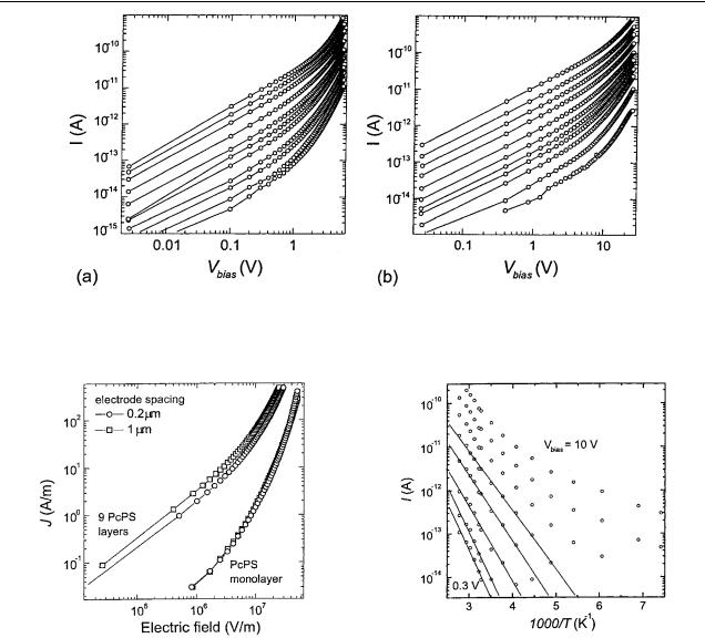
A similar set of current–voltage curves was measured for samples with nine layers of PcPS (figure 5). Qualitatively, the curves appear very similar to those of the samples with a single monolayer of PcPS. The ohmic regime at low voltages is more clearly revealed, due to the higher current level. Due to
1046
Electronic transport in monolayers of phthalocyanine polymers
Figure 5. Current–voltage characteristics of nine PcPS layers on top of interdigitated electrodes with spacings of 0.2 µm (a) and 1 µm (b). The curves are taken at regular intervals of 19 K between 135 and 360 K. At low bias, the curves are linear. The nonlinear regime is qualitatively the same as for the monolayer samples, but less pronounced. Again the leakage conductivity of (5 × 10¹⁶ )−1 was subtracted from the original data.
Figure 6. Comparison of the current density as a function of applied field for the four samples at a temperature of 310 K. The overlap between curves taken for different electrode spacings confirms the V/L scaling of the current density, as predicted in equation (2). The higher current level of the nine-layer samples is attributed to a higher level of remnant dopants.
the limited voltage range over which the nonlinear component of the current has been measured for these samples, accurate deduction of the fitting parameters through fits of equation (2) is not possible.
We now compare current–voltage curves of the four different samples at one temperature (310 K). Figure 6 shows the current density versus the applied field. The curves taken for different electrode spacings do overlap in this graph. The current density thus appears to be a function of V/L, in agreement with equation (2). The difference between the curves for a different number of PcPS layers may be explained in terms of remnant doping. As will be discussed in section 3.6, the doping level of the PcPS is strongly dependent on the ambient pressure and time in vacuum prior to measuring. The dedoping of the nine-PcPS-layer samples is slower than that of the single-PcPS-monolayer samples, resulting in a higher
Figure 7. Current versus 1000/ T for various bias voltages. At low bias, the dependence is well described by thermal activation (straight lines). At higher bias deviations are observed.
doping level and corresponding higher conductivity for the nine-PcPS-layer samples.
5. Temperature dependence
We investigate the effect of the temperature on the conductivity by plotting current versus 1/ T for different bias voltages of the monolayer sample with an electrode spacing of 0.2 µm (figure 7). Other samples qualitatively show the same characteristics. The data taken at low bias follow a simple thermally activated behaviour I exp(− E/ kBT ) (straight lines). At higher bias and higher temperature, the curves deviate from such a behaviour. We cannot therefore define an activation energy E in the strict sense. However, the derivative of the curves in figure 7 still does indicate a characteristic energy scale E that dominates the conduction process at a certain temperature. This derivative is plotted as a function of applied electric field in figure 8. In the
1047
S J Tans et al
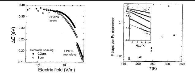
Figure 8. Effective activation energy E at 260 K as a function of applied electric field for different electrode spacings.
ohmic regime at low bias, the activation energy is expected to be independent of bias voltage. From figure 8, E indeed appears to be constant for lower bias voltages at a value of 0.38 eV. At higher applied fields, E decreases linearly with ln V , as is predicted for E = Evb − Ef in the SCLC model (equation (6)). From the field dependence of E we can again determine Fm and Tc using equation (6). For the monolayer samples we find Fm = 1.6 × 10⁸ V m−1 and Tc = 1.6 × 10³ K and Fm = 1.9×10⁸ V m−1 and Tc = 1.5×10³ K, for electrode spacings of 0.2 and 1.0 µm, respectively. These values are in excellent agreement with the values found from the fits of the I–V curves in the previous section (see table 1). The asymptote of the curves of the nine-layer samples in figure 8 is less defined because of the limited voltage bias range. The trends of the oneand nine-layer samples, however, seem to be similar. The values of Fm and Jm may be used to deduce the trap density Ntot (equation (4)) and µNv (equation (5)). We
find Ntot = 1.2 × 1025 m−3, which corresponds to one trap per 63 Pc monomers and µNv = 5.2 × 10¹⁵ m−1 V−1 s−1. When
we estimate Nv to equal about one electron state per monomer, the resulting value for µ becomes 6 × 10⁻¹² m2 V−1 s−1.
The inset of figure 9 shows that E is not constant with temperature. It appears that the relation between E and ln V is linear for all temperatures, in agreement with in the SCLC model. The deviations from a simple thermally activated behaviour (figure 7) may be the result of a temperaturedependent trap density. In figure 9 the trap density resulting from fits at various temperatures is displayed. The trap density appears to increase with increasing temperature (figure 9). NMR studies have shown that the Pc monomer discs in the PcPS polymer make rotational jumps around the main axis at RT [3]. The frequency of these rotations is found to increase with increasing temperature. Since rotations have a dramatic effect on the electronic overlap between monomers [11], this may lead to localized states.
The above SCLC model considers charge transport through thermal activation of holes from localized states at trap sites to extended states in the valence band. Alternatively, the holes may contribute to the current by hopping from trap to trap. The temperature dependence of the current is then described by the variable-range-hopping (VRH) model. This
Figure 9. Trap density versus temperature for samples of one monolayer with an electrode spacing of 0.2 µm (solid dots) and 1.0 µm (circles). The trap density was obtained from fits of E
versus ln(Vbias), cf equations (4) and (6). The E versus ln(Vbias) data are displayed in the inset. They show a linear dependence for
all temperatures.
predicts a dependence of I exp(T0/ T )a , where a < 1. This functional form indeed approaches the experimental data somewhat better than the thermal activation model. It cannot however produce a satisfactory fit over the entire temperature range.
6. Chemical doping and field effect
In an effort to increase the conductivity of the pristine PcPS films, we have investigated the effects of chemical doping with oxygen and iodine and the field effect. As a preparation for the O2 doping, samples were degassed for a standard period of 48 h in the evacuated sample chamber. Subsequently the samples were exposed to 1 bar of O2 pressure for 24 h. After the latter, we observed an increase of the conductivity of about two orders of magnitude with respect to the value in vacuum. The sample chamber is then evacuated again to evaluate the dedoping process. In figure 10 the current through a monolayer sample and a nine-PcPS-layer sample is plotted as a function of evacuation time. No saturation of the dedoping process is observed, even after prolonged outgassing. However, the remaining dedoping process after such an outgassing treatment is negligible within the time it takes to measure the kinds of dataset presented in the previous sections. Comparing the two samples, we observe the dedoping rate to be about ten times faster for the PcPS monolayer sample than for the nine-PcPS- layer sample. This explains the different conductivity levels for samples 1 and 2 found in the current–voltage curves of figure 6. We did not observe a significant effect of I2 vapour on the conductivity. Apparently, the chemical doping with iodine is not effective with our LB-prepared monolayers of PcPS.
The effect of the O2 doping is readily understood. The fact that it acts as a dopant for Pc monomers has been shown before [11]. The O−2 counter-ions are incorporated in the PcPS film and shift the Fermi energy towards the valence band, thereby increasing the conductivity. We do not have an explanation for the absence of an effect on the I2 vapour.
1048

Electronic transport in monolayers of phthalocyanine polymers
Figure 10. Current through a sample of one monolayer (bottom curve) and nine monolayers (top curve) as a function of time upon evacuation of the sample chamber after a 24 h exposure to oxygen. Electrode spacing is 0.2 µm and Vbias = 5 V.
I2 is known to be a very effective dopant for [Si(Pc)O]n bulk material [11], increasing its conductivity by at least five orders of magnitude. One may speculate that the I3− counter-ions cannot easily be accommodated near the PcPS due to the steric hindrance of the alkane side chains on the PcPS.
In a three-terminal configuration, a voltage on a third gate electrode may be used to shift the Fermi energy. Such a field effect can be an alternative way to modulate the conductivity. To investigate the effect of an externally applied electric field, samples with a gate were realized by using highly doped Si wafers with a 100 nm thick SiO2 layer as substrate. Upon application of a gate voltage (Vg) on the substrate, charge will be induced in the PcPS layer. The induced charges will fill up trap states within the bandgap, resulting in a shift of the Fermi energy towards the valence band. From the parameters we found for the exponential trap distribution, we can estimate the gate voltage necessary to fill up all the traps up to the valence band, i.e. for shifting the Fermi energy to the edge of the valence band. We calculate that this should be the case for Vg ≈ −17 V. The maximum possible voltage that could be applied before breakdown between the source or drain electrodes and the gate electrode, was found to be around 50 V. In figure 11 the current through a monolayer sample is plotted as a function of time t. At t = 0 s, a gate voltage of −25 V is applied. A large current increase of more than three orders of magnitude is observed. This however drops off fairly quickly. The initial positive current increase cannot be explained by leakage currents or charging of capacitances (e.g. between gate and source–drain electrodes). Such currents would be in the opposite direction. Indeed, when no bias voltage is applied we do not observe a positive current peak (see inset) when the gate voltage is switched on. We therefore conclude that the increase has to be attributed to a field effect. The strong decrease of the effect in time renders it useless however. The decrease is so strong that after about 1.5 h only a factor of three increase in the conductivity is left. A re-ordering of possible remnant dopants (such as O−2 ) that effectively screen the electric field may provide an explanation for the observed current decrease on such long timescales.
Figure 11. Current through a PcPS monolayer on top of electrodes with a 0.2 µm spacing at a bias of 4 V as a function of time. At
t = 0 s the gate voltage is changed from 0 to −25 V. The very large current increase indicates a strong field effect. The subsequent degradation of the current, however, makes it unsuitable as a practical tool to vary the conductivity in the PcPS layer. Inset, similar measurement on an electrode structure without a deposited PcPS film. At t = 0 s, the gate voltage is switched on. At
t ≈ 1600 s it is switched off. Here no positive current curve is observed, indicating that the strong current increase in the main figure indeed results from the PcPS layer.
7. Conclusions
The electronic transport properties of monolayers of PcPS molecular wires on top of interdigitated nano-electrodes has been investigated. At low applied bias voltages, we find that the conductivity is ohmic. At high bias voltage the current is spacecharge limited. This model describes the effect of a spacecharge injection into materials with considerable bandgaps, a low concentration of charge carriers and an exponential trap distribution. From the model we obtain a total trap density of 1.2 × 1025 m−3 and a exponential drop-off rate of 1500 K.
The resistivity of the undoped PcPS layers at RT is about 1 × 109 cm. For an individual PcPS molecule of 20 nm length, this would yield a current of 5×10⁻¹⁸ A at a bias voltage of 1 V, which is a number of orders too low to be detectable. For the study of individual molecules, we thus need to increase the conductivity of these semiconducting molecules. Some first efforts in this direction have not yielded the desired increase. In an O2 ambient, a two-order increase of the conductivity is found. An iodine vapour ambient appears to have no effect on the conductivity. We do observe an initial field-effect-induced increase in the conductivity in monolayer samples of three orders of magnitude. This however decreases with time.
Acknowledgments
We thank Hans Mooij for support and B van den Enden for technical assistance. The work was supported by the Dutch Foundation for Fundamental Research on Matter (FOM).
References
[1]Schumm J S, Pearson D L and Tour J M 1994 Angew. Chem. Int. Edn Engl. 33 1360
[2]Bauerle¨ P 1992 Adv. Mater. 4 102
[3]Wegner G 1993 Mol. Cryst. Liq. Cryst. 235 283
1049

S J Tans et al
[4] Dimitrakopoulos C D and Malenfant P R L 2002 Adv. Mater. |
[9] |
Wu J, Lieser G and Wegner G 1996 Adv. Mater. 8 151 |
14 99 |
|
Wu J, Lieser G and Wegner G 1996 Macromolecules 29 1844 |
[5] Ye J, Chen H Z, Shi M M and Wang M 2003 Prog. Nat. Sci. |
[10] |
Tans S J, Geerligs L J, Dekker C, Wu J and Wegner G 1997 |
13 81 |
|
J. Vac. Sci. Technol. B 15 586 |
[6] Aviram A (ed) 1992 Molecular Electronics—Science and |
[11] |
Marks T J 1990 Angew. Chem. Int. Edn Engl. 29 |
Technology (AIP Conf. Proc. vol 262) (New York: |
|
857 |
American Institute of Physics) |
[12] |
Lampert M A and Mark P 1970 Current Injection in Solids |
Carter F L, Siatkowski R E and Wohltjen H (ed) 1988 |
|
(New York: Academic) |
Molecular Electronics Devices (Amsterdam: |
[13] |
Lanyon H P D 1963 Phys. Rev. 130 134 |
North-Holland) |
[14] |
Sussman A 1967 J. Appl. Phys. 38 2738 |
[7] Ferencz A, Armstrong N R and Wegner G 1994 |
[15] |
Hack M, Tuan H, Shur M and Yap P 1987 Mater. Res. Symp. |
Macromolecules 27 1517 |
|
Proc. 95 457 |
[8] Hanack M and Lang M 1994 Adv. Mater. 6 819 |
[16] |
Wegner G, unpublished |
1050