

INSTITUTE OF PHYSICS PUBLISHING |
NANOTECHNOLOGY |
Nanotechnology 17 (2006) 2279–2283 |
doi:10.1088/0957-4484/17/9/035 |
Study of charge transport in conducting polymer between electrodes with nanogaps
Tsu-Hsien Ku1, Ju-Hung Hsu1, Heh-Nan Lin1,4, Hsin-Fei Meng2,
Ming-Chih Chen3 and Show-An Chen3
1Department of Materials Science and Engineering, National Tsing Hua University, Hsinchu 300, Taiwan
2Institute of Physics, National Chiao Tung University, Hsinchu 300, Taiwan
3Department of Chemical Engineering, National Tsing Hua University, Hsinchu 300, Taiwan
E-mail: hnlin@mx.nthu.edu.tw
Received 30 September 2005, in final form 7 February 2006
Published 7 April 2006
Online at stacks.iop.org/Nano/17/2279
Abstract
We report the study of charge transport in the conducting polymer MEH-PPV between Au electrodes with nanogaps created by atomic force microscopy nanoscratching. Two different types of charge transport, namely space-charge-limited and Ohmic conductions, are observed. For the former case, a high mobility of around 1 cm2 V−1 s−1 at a field of 106 V cm−1 is obtained. For the latter case, a high conductivity of around 10 S cm−1 is obtained and a lower limit mobility of around 5 cm2 V−1 s−1 is calculated. The origin of this unusual result is not clear, but it may be due to the formation of single-crystalline domains between the electrodes, that facilitates three-dimensional band transport.
1. Introduction
Charge transport in conjugated polymers has been the focus of extensive research activities in recent years due to the great potential of plastic electronics [1–3]. In particular, regioregular poly(3-hexylthiophene) (P3HT) based field-effect transistors (FETs) have been studied in great detail since high mobilities up to 0.2 cm2 V−1 s−1 were reported [4, 5]. In addition, a mobility increase has also been observed as the channel length is reduced in the micrometre regime [5]. When the length is further reduced down to the nanoscale regime, however, much lower mobilities have nevertheless been obtained [6]. Although the origin is not clear, this peculiar behaviour may be due to short channel effects that invalidate the mobility analysis [7].
On the other hand, reports of FETs based on poly[2- methoxy, 5-(2 -ethyl-hexyloxy)- p-phenylene vinylene] (MEHPPV) [3, 8–10] are relatively scarce, despite the extensive use of this polymer for light-emitting diodes (LEDs) [1, 9, 11]. The main reason is the low mobilities of around 10−6 cm2 V−1 s−1 obtained from previous charge transport studies of MEH-PPV LEDs [1, 11], of which the value is a few orders of magnitude less than those of P3HT. However, the reported mobilities are from vertical structures as in LEDs, and horizontal structures as in FETs actually exhibit higher mobilities. In fact, field-
4 Author to whom any correspondence should be addressed.
effect mobilities higher than 10−4 cm2 V−1 s−1 have been found [3, 9], of which the value is two orders of magnitude higher than those in vertical structures. Furthermore, an
even higher mobility |
of 0.01 |
cm2 V−1 s−1 |
at a field of |
5 × 10⁵ V cm−1 has |
been |
observed in a |
two-terminal |
geometry [10]. The dramatic difference between the vertical and the horizontal mobility is due to the facts that the chain alignment is parallel to the substrate [10, 12–14] and charge transport along the backbones of the chains is much faster than across the chains [12].
Since electron and hole mobilities as high as 0.5 cm2 V−1 s−1 have been reported on single MEH-PPV chains [15], it is of great interest to investigate whether such high mobilities can be obtained in a horizontal structure when the electrodes are separated with a nanogap. In this paper, we report the study of hole transport in MEH-PPV deposited between Au electrodes with gaps ranging from 240 down to 50 nm. The results reveal that an appreciable mobility enhancement appears as the gap is reduced, and, more significantly, mobilities of more than around 5 cm2 V−1 s−1 can actually be obtained at sub-100 nm gaps.
2. Experiment
The electrodes were fabricated on glass substrates by a combination of atomic force microscopy (AFM) nanoscratching
0957-4484/06/092279+05$30.00 © 2006 IOP Publishing Ltd Printed in the UK |
2279 |
T-H Ku et al
(a) |
(b) |
|
|
1 m |
|
100 nm |
|
|
|||
(c) |
|
(d) |
||
|
||||
|
|
|||
100 nm |
100 nm |
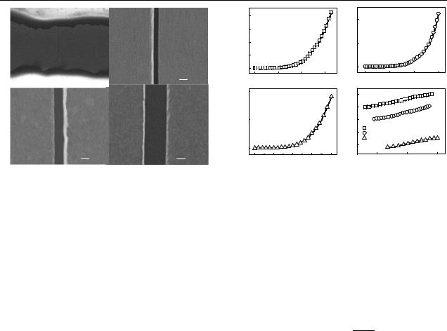
Figure 1. SEM images of (a) a pair of nanoelectrodes with a width of 4.2 µm, and various nanogaps with lengths of (b) 50, (c) 100, and (d) 240 nm. Note that (a) appears blurred due to the charging effect on the glass substrate.
and lift-off process [16]. Briefly, a 50 nm thick PMMA film was first prepared on a glass substrate by spin-coating. Two large contact pads and a groove were created on the film by scratching with a blunt tip. After coating an Au film and performing lift-off, a pattern with a width on the order of 5 µm was produced. By using a new tip to scratch on the Au stripe, a pair of electrodes with a nanogap was generated. The gap length was then characterized by scanning electron microscopy (SEM). The thicknesses of the electrodes ranged between 10 and 20 nm.
Four MEH-PPV (average molecular weight 450 kg mol−1) solutions with concentrations of 1.5, 1.5 × 10⁻¹, 1.5 × 10⁻², and 1.5 × 10⁻³ mg ml−1 were prepared in chloroform. The substrates with the electrodes were baked at 120 ◦C for 10 min, and MEH-PPV films were then produced by drop-casting the solutions onto the substrates in air or nitrogen gas in a dark environment. The thicknesses of the films were maintained at around 150 nm by controlling the number of drops. Electrical measurements were realized by using a Keithley 2400 sourcemeasure unit under similar conditions as the films were made. Prior to each drop-casting, the leakage current between the employed electrodes was measured and it was always at the noise level.
3. Results and discussion
The SEM image of a typical pair of electrodes is shown in figure 1(a). (Note that the image appears blurred outside the electrodes due to the charging effect on the glass substrate.) The zoomed images of various nanogaps with widths ranging from 50 to 240 nm are shown in figures 1(b)–(d). The current– voltage (I –V ) curves for three samples with a dilution ratio of 1.5 × 10⁻³ mg ml−1 deposited at various electrodes are shown in figures 2(a)–(c). The nonlinear behaviour of the curves at high fields indicates a space-charge-limited (SCL) conduction that has been observed in either a vertical [1, 10, 11] or a horizontal [10, 17] structure and can be described by
|
20 (a) |
|
|
|
|
|
|
(b) |
|
|
|
(A) |
|
|
|
|
|
|
(A) |
2 |
|
|
|
15 |
|
|
|
|
|
|
|
|
|
||
Current |
5 |
|
|
|
|
|
Current |
1 |
|
|
|
|
10 |
|
|
|
|
|
|
|
|
|
|
|
0 |
|
|
|
|
|
|
0 |
|
|
|
|
0 |
2 |
4 |
|
6 |
|
|
0 |
3 |
6 |
9 |
|
|
Voltage (V) |
|
|
|
|
|
Voltage (V) |
|
||
|
14 (c) |
|
|
|
|
|
100 (d) |
|
|
||
(nA) |
|
|
|
|
|
/Vs) |
|
|
|
|
|
Current |
|
|
|
|
|
(cm |
|
−2 |
|
|
|
|
7 |
|
|
|
|
2 |
10 |
|
|
|
|
|
|
|
|
|
|
|
|
|
- 70 nm |
|
|
|
|
|
|
|
|
|
|
|
- 100 nm |
|
|
|
|
|
|
|
|
|
|
|
- 200 nm |
|
|
|
0 |
|
|
|
|
|
10−4 |
|
|
|
|
|
|
|
|
|
|
|
|
|
|
|
|
|
0 |
5 |
10 |
15 |
20 |
|
|
|
600 |
800 |
1000 |
|
|
Voltage (V) |
|
|
|
|
E1/2 [(V/cm)1/2] |
|
|||
Figure 2. Results for three samples made from the
1.5 × 10⁻³ mg ml−1 solution. (a)–(c) I –V curves for the samples with the gaps of 70, 100, and 200 nm, respectively, and (d) the corresponding P–F plots of µ versus E 1/2 at high fields.
equation (1), |
|
|
V 2 |
|
J = |
9 |
εrε0µ |
(1) |
|
|
|
|||
8 |
L3 |
where |
J is the current density, εr |
the dielectric constant, |
ε0 the |
vacuum permittivity, µ the |
mobility, V the applied |
voltage, and L the gap of the electrodes. In addition, the mobility is also known to obey the Poole–Frenkel (P–F) relationship [11, 18, 19] as described by equation (2),
µ = µ0 exp E /E0 (2)
where µ0 is the zero-field mobility, E the electric field (equal to V /L), and E0 the field coefficient.
By using an εr of 3 [14], the mobilities can be calculated from equation (1)N ot e 5 and the corresponding P–F plots are shown in figure 2(d). For the 70 and 100 nm samples, the mobilities are four orders of magnitude higher than those from vertical structures [10, 11] and two orders of magnitude higher than results from our previous conducting AFM investigation of nanoscale vertical transport in a 30 nm thick film [20] due to faster in-plane charge transport as mentioned earlier. A significant result is that the mobility reaches 1 cm2 V−1 s−1 at a field of 106 V cm−1 for the 70 nm gap sample (see footnote 5). This value is comparable to the single chain hole mobility of 0.2 cm2 V−1 s−1 reported in the literature [15].
From figure 2(d), it is clear that the mobility increases as the gap is reduced and the reduction in the nanoscale regime reported in the literature [6] does not appear. The mobility increase can be explained by the following argument. It is known that ordered crystalline domains separated by amorphous regions are present in MEH-PPV films [13]. The field dependent mobility as described by equation (2) is a result of hopping between different energy levels, which are also spatially correlated, in these domains [18, 19]. As the gap
5 It should be noted that the current density is calculated by considering the current flows through an area defined by the width and the thickness of the electrodes. This may create a potential error in the calculated current densities, mobilities and conductivities since the polymer thickness is roughly 10 times the electrode thickness.
2280
Study of charge transport in conducting polymer between electrodes with nanogaps
is reduced, the variation in the energy levels decreases and consequently a higher mobility is obtained.
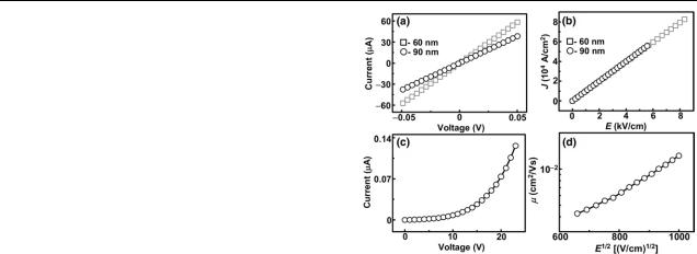
For samples prepared from the 1.5 mg ml−1 solution with sub-100 nm gaps, dramatically different I –V curves were obtained. It was found that the current was quite low when the voltage was below roughly 0.5 V. A current surge with a value of around 0.5 mA then appeared randomly when the voltage was increased from 0.5 to 1 V. After the observation of this phenomenon, a voltage sweep from 0 to 1 V was first applied to the tested sample and the voltage was reduced to zero immediately to avoid sample damage. After the first voltage sweep, in which a current surge occurred, a new I –V curve was measured. The curve was found to be reproducible and the current surprisingly increased by orders of magnitude (see below). It was also verified that the high current was not caused by shorts in electrodes since one of the samples was rinsed in chloroform to remove the polymer and the current again returned to noise level. Apparently, the first voltage sweep produced irreversible change in the polymer and consequently the electrical behaviour.
The reproducible I –V curves of two representative samples are shown in figure 3(a) and they both exhibit Ohmic conduction. The conductivities of these samples can be derived from the curves from the Ohm’s law shown in equation (3),
J = σ E = neµE |
(3) |
where σ is the conductivity and n the carrier density. |
The |
J –E plots are shown in figure 3(b) and the conductivities are surprisingly high with values of around 10 S cm−1 (see footnote 5). The implication of such high conductivities will be discussed later. For samples with larger gaps, on the other hand, the current surge did not happen and the SCL conduction appeared. The I –V curve and the P–F plot for a sample with a gap of 230 nm are shown in figures 3(c) and (d), respectively. Furthermore, the mobilities are less than those from the 70 and 100 nm gap samples shown in figure 2. In order to eliminate the influences of oxygen and moisture, different samples were prepared and measured in nitrogen gas. The results are similar to those obtained in air and ascertain that the electrical behaviour is little influenced by exposure in air.
More samples were prepared from two other solutions and their I –V curves were also measured and analysed. A summary of the electrical characteristics of representative samples along with the corresponding dimensions of the nanoelectrodes is listed in table 1. (It should be noted that the conductivities of the Ohmic samples were calculated
from the reproducible I –V |
curves after first voltage sweeps |
as mentioned previously.) |
It is clear that the conduction |
behaviour is strongly dependent on the solution concentration and the electrode gap. The former factor is known to affect film morphology significantly and thus the electrical behaviour [21, 22], and the latter may also have a similar effect.
The µ0 and the E0 for the samples revealing SCL conduction can be calculated from P–F plots based on
equation (1) and |
are also listed in table 1. |
|
It is |
||||||
evident that the values of |
E0 |
are in |
reasonable |
agreement |
|||||
with macroscopic |
results |
|
5 |
× |
104 |
V cm−1) |
from |
both |
|
( |
|
||||||||
vertical [10, 11] and horizontal structures [10] |
and |
also |
|||||||
our previous study |
of vertical transport within a |
|
nanoscale |
||||||
Figure 3. Results for three samples made from the 1.5 mg ml−1 solution. (a) I –V curves after first voltage sweeps (see text) for two samples with gaps of 60 and 90 nm, and (b) the corresponding J –E curves. (c) I –V curves for a sample with a gap of 230 nm, and (d) the corresponding P–F plot of µ versus E 1/2 at high fields.
confinement [20]. This is a reasonable consequence since E0 is mainly dependent on temperature for the same material from studies of mobility dependence on electric field and temperature [1]. On the other hand, the values of µ0 vary by orders of magnitude (10−6–10−3 cm2 V−1 s−1) and are much higher than macroscopic results ( 2 × 10⁻⁷ cm2 V−1 s−1) from vertical structures [11], but comparable to results ( 10−5 cm2 V−1 s−1) from horizontal structures [10]. The large variation in µ0 simply reflects the significant influence of film morphology on charge transport [21, 22].
For the Ohmic samples listed in table 1, the high conductivities of around 10 S cm−1 indicate either large carrier densities or mobilities from equation (3). At first sight, the carrier densities of all the studied samples are on the same order of magnitude in the low field regime since background p-type carriers are generated in the synthesis of MEH-PPV. In the low field regime, the conductivity of an SCL sample can be found from its I –V curve. Its carrier density can then be calculated from equation (3) by taking the mobility equal to the zero-field mobility. Based on this idea, the low field conductivities for the
I –V |
1 |
× |
10−4 |
curves in figures 2(a) and 3(c) are found to be 8.0 |
|
and 1.2 × 10⁻⁵ S cm− , respectively, and the calculated carrier densities are 1018 and 1017 cm−3, respectively. Taking a carrier density of 5 × 1017 cm−3, the mobilities of the Ohmic samples would be on the order of 100 cm2 V−1 s−1 (see footnote 5).
On the other hand, the extremely large value of mobility seems unlikely and it is possible the carrier density for an Ohmic sample has increased significantly after the first voltage sweep. An accurate determination of the carrier density is not easy but the upper limit is around 1019 cm−3 [23], which is roughly 1% of the monomer density. (The volume of a monomer unit cell is 0.712 × 1.605 × 0.647 nm3 and corresponds to a monomer density of 1.35 × 1021 cm−3 [13].) With this carrier density, mobilities of around 5 cm2 V−1 s−1 are obtained for the Ohmic samples (see footnote 5). This value is again higher than single chain mobility [15] and results from regioregular P3HT [4, 5].
As can be seen in table 1, the Ohmic behaviour occurs only in electrodes with gaps of less than around 100 nm. This
2281

T-H Ku et al
Table 1. A summary of the electrical properties of representative samples and the corresponding gap lengths of the nanoelectrodes (see footnote 5). It should be noted that the conductivities of the Ohmic samples were calculated from reproducible I –V curves after first voltage sweeps as mentioned in the text.
Concentration |
|
Gap |
Conduction |
µ0 (cm2 V−1 s−1) |
|
|
|||||
(mg ml−1) |
Atmosphere |
(nm) |
behaviour |
E0 (V cm−1) |
σ (S cm−1) |
||||||
|
|
|
|
60 |
Ohmic |
— |
|
|
9.92 |
|
|
|
|
|
|
90 |
|
|
10.02 |
|
|||
|
|
|
Air |
|
|
|
|
|
|
||
|
|
|
|
|
|
|
|
|
|
|
|
|
|
|
|
230 |
SCL |
4.50 |
× |
10−4 |
— |
||
|
|
|
|
|
|
4 |
|||||
1.5 |
|
|
|
|
|
9.07 × |
10 |
|
|
|
|
|
|
|
|
50 |
Ohmic |
— |
|
|
5.67 |
|
|
|
|
|
|
85 |
|
|
8.08 |
|
|||
|
|
|
N2 |
|
|
|
|
|
|
||
|
|
|
|
|
|
|
|
|
|
|
|
|
|
|
240 |
SCL |
2.84 |
× |
10−5 |
— |
|||
|
|
|
|
||||||||
|
|
|
|
|
10 |
4 |
|||||
|
|
|
|
|
|
4.81 × |
|
|
|
||
1.5 |
× |
10−1 |
Air |
55 |
Ohmic |
— |
|
|
10.28 |
|
|
|
|
|
|
||||||||
1.5 × 10⁻² |
Air |
85 |
SCL |
6.29 |
× |
10−3 |
— |
||||
5.31 |
104 |
||||||||||
|
|
|
|
|
|
|
× |
|
|
|
|
|
|
|
|
70 |
|
4.82 |
× |
10−3 |
|
|
|
|
|
|
|
|
|
10 |
4 |
|
|
||
|
|
|
|
|
|
3.12 × |
|
|
|
||
1.5 × 10⁻³ |
Air |
100 |
SCL |
2.08 |
× |
10−4 |
— |
||||
2.34 |
104 |
|
|
||||||||
|
|
|
|
|
|
|
× |
10−6 |
|
|
|
|
|
|
|
200 |
|
1.41 |
× |
|
|
||
|
|
|
|
|
|
10 |
4 |
|
|
||
|
|
|
|
|
|
3.13 × |
|
|
|
||
tendency is not understood at this stage. However, a possible explanation is that a nanogap acts as a shallow nanotrench and facilitates the formation of larger crystalline domains inside. In the first voltage sweep, the current surge has an annealing effect and transforms the domains between the electrodes into a single-crystalline domain. A three-dimensional band transport consequently appears [2] due to the large interchain π -orbital overlap in the single-crystalline domain. Indeed, it has been shown that interchain transport [4] is even faster than intrachain transport [24] for self-assembled P3HT. When the gap is increased, on the other hand, smaller domains are formed and the first voltage sweep has no effect. As a result, the mobility decreases significantly due to trapping at boundaries and the SCL behaviour appears.
4. Conclusion
To summarize, the study of charge transport in the conducting polymer MEH-PPV deposited between Au electrodes with nanogaps is reported. The electrodes are fabricated by AFM nanoscratching and have gaps ranging between 50 and 240 nm. Two different types of charge transport, i.e. SCL and Ohmic conductions, are observed. For the SCL samples, a high mobility of around 1 cm2 V−1 s−1 at 106 V cm−1 is obtained. For the Ohmic samples, high conductivities of around 10 S cm−1 are obtained and mobilities with a lower limit of around 5 cm2 V−1 s−1 are calculated. The origin of this unprecedented value of mobility is not clear, but it is likely due to the formation of single-crystalline domains between the electrodes, that facilitates three-dimensional band transport. The present work also provides important information for the construction of high current density organic devices.
Acknowledgment
This work was supported by the Ministry of Education, Program of Academic Excellence, under grant No 91-E-FA04- 2-4A.
References
[1]Blom P W M and Vissenberg M C J M 2000 Mater. Sci. Eng. R
27 53
[2]Dimitrakopoulos C D and Malenfant P R L 2002 Adv. Mater.
14 99
[3]Scheinert S and Paasch G 2004 Phys. Status Solidi a 201 1263
[4]Sirringhaus H et al 1999 Nature 401 685
[5]Wang G, Swensen J, Moses D and Heeger A J 2003 J. Appl. Phys. 93 6137
[6]Mas-Torrent M, den Boer D, Durkut M, Hadley P and Schenning A P H J 2004 Nanotechnology 15 S265
[7]Austin M D and Chou S Y 2002 Appl. Phys. Lett. 81 4431
[8]Shaked S, Tal S, Roichman Y, Razin A, Xiao S, Eichen Y and Tessler N 2003 Adv. Mater. 15 913
[9]Tzeng K L, Meng H F, Tzeng M F, Chen Y S, Liu C H, Horng S F, Chang S M, Hsu C S and Chi C C 2004 Appl. Phys. Lett. 84 619
[10]Meng H F, Chen B L, Tzeng K C and Horng S F 2006 Appl. Phys. Lett. 88 023505
[11]Bozano L, Carter S A, Scott J C, Malliaras G G and
Brock P J 1999 Appl. Phys. Lett. 74 1132
[12]McBranch D, Campbell I H, Smith D L and Ferraris J R 1995
Appl. Phys. Lett. 66 1175
[13]Yang C Y, Hide F, Diaz-Garcia M A, Heeger A J and
Cao Y 1998 Polymer 39 2299
[14]Tammer M and Monkman A P 2002 Adv. Mater. 14 210
[15]Hoofman R J O M, de Haas M P, Siebbeles L D A and Warman J M 1998 Nature 392 54
[16]Chen Y-J, Hsu J-H and Lin H-N 2005 Nanotechnology 16 1112
[17]Paasch G, Lindner T, Rost-Bietsch C, Karg S, Riess W and Scheinert S 2005 J. Appl. Phys. 98 084505
[18]Gartstein Y N and Conwell E M 1995 Chem. Phys. Lett.
245 351
2282

Study of charge transport in conducting polymer between electrodes with nanogaps
[19]Rakhmanova S V and Conwell E M 2000 Appl. Phys. Lett. 76 3822
[20]Lin H-N, Lin H-L, Wang S-S, Yu L-S, Perng G-Y,
Chen S-A and Chen S-H 2002 Appl. Phys. Lett. 81 2572 [21] Nguyen T-Q, Martini I B, Liu J and Schwartz B J 2000 J. Phys.
Chem. B 104 237
[22]Liu J, Shi Y, Ma L and Yang Y 2000 J. Appl. Phys. 88 605
[23]Pinner D J, Friend R H and Tessler N 1999 J. Appl. Phys. 86 5116
[24]Grozema F C, Siebbeles L D A, Warman J M, Seki S, Tagawa S and Scherf U 2002 Adv. Mater. 14 228
2283