

nanotechnology / nano4_7_057
.pdfINSTITUTE OF PHYSICS PUBLISHING |
NANOTECHNOLOGY |
Nanotechnology 15 (2004) S483–S488 |
PII: S0957-4484(04)75635-4 |
Temperature effects on conduction through a molecular junction
Yoram Selzer1,3, Marco A Cabassi2, Theresa S Mayer2,3
and David L Allara1,3
1Department of Chemistry and the Materials Research Institute, Pennsylvania State University, University Park, PA 16802, USA
2Department of Electrical Engineering, Pennsylvania State University, University Park, PA 16802, USA
E-mail: yus1@psu.edu, tsm2@psu.edu and dla3@psu.edu
Received 18 November 2003
Published 17 May 2004
Online at stacks.iop.org/Nano/15/S483
DOI: 10.1088/0957-4484/15/7/057
Abstract
The measured effect of temperature on charge transport through individual chemisorbed 1-nitro-2,5-di(phenylethynyl-4 -mercapto)benzene molecules spanning a gold electrode gap is reported for the range of 10–300 K.
Conduction is dominated by coherent superexchange at low temperatures and shifts to an incoherent hopping process above bias-dependent temperature thresholds. The results are consistent with proposed theoretical mechanisms in which bias-dependent heat dissipation from inelastic vibrational scattering within the molecule raises the temperature of the junction above that of the surrounding system, which in turn leads to the shift in the prevailing conduction process with increasing bias.
(Some figures in this article are in colour only in the electronic version)
1. Introduction
The recent surge of activity in molecular electronics is driven by expectations of scientific inroads into the realm of the molecular state and by the anticipation of a high technological payoff [1, 2]. Continued progress in this area depends critically on developing a thorough understanding of the fundamental processes of charge conduction through individual or small assemblies of molecules connected between two reservoirs of charge carriers, usually metallic leads. This understanding relies on concepts and theoretical methodologies that have been developed and applied to study molecular charge transfer in donor–bridge–acceptor systems [3–10]. Indeed, the relationship between a given bridge-assisted charge transfer rate and the corresponding zero-bias molecular conduction of the same molecular species has already been discussed [11, 12]. Conduction proceeds through molecular bridges by two distinct mechanisms [11–17]. When the bridge energy and the Fermi level offset is greater than kT , the role of the bridge is simply to mediate the electronic coupling between
3 Authors to whom any correspondence should be addressed.
the two leads. In this so-called superexchange regime [18], charge tunnels between the two metal leads, resulting in a bridge population that is negligible. In contrast, when the bridge energy and the Fermi level are closer than kT , conduction takes place by populating the bridge states with charge carriers and diffusive hopping of those carriers on the bridge. The transition between these two conduction regimes and their dependence on general attributes such as dephasing, disorder and relaxation, as well as on experimentally accessible parameters such as temperature and bridge length, are currently the subject of active theoretical and experimental research [3– 19].
Most experimental research aimed at addressing these fundamental issues is based on measurements of donor– bridge–acceptor systems in solution [7] and electrochemical studies of monolayers with specified bridge, tethered with a redox species, that are assembled on a metal electrode [19]. Metal–molecule–metal configurations offer several advantages over such solution-based experiments:
(i)They enable ‘communication’ with single molecules, thus completely eliminating ensemble averaging.
0957-4484/04/070483+06$30.00 © 2004 IOP Publishing Ltd Printed in the UK |
S483 |
Y Selzer et al
(ii)They can be performed at very low temperatures, where vibrations are not excited and rotations are hindered, allowing one to elucidate their role in the charge transfer process.
(iii)They eliminate the effect of solvent and electrolyte on reorganization energy that, in principle, should make theoretical estimates of this parameter more precise.
(iv)They allow adjustments in energy alignment across the molecular bridge by changing the potential on the metal leads.
A priori control of the last parameter in donor–bridge–acceptor systems relies on laborious synthesis to attach different donors or acceptors to a given bridge to cover a wide range of energy alignments [7]. Despite these advantages, and although several methods have been demonstrated for fabricating single molecule junctions [20–28], systematic studies of conduction through conjugated oligomers remain relatively scarce [29– 36].
Recently, we began to investigate the role of thermally
activated |
conduction in |
conjugated molecules that span |
a gold |
electrode gap. |
We observed a temperature- |
induced transition between coherent tunnelling and thermally activated incoherent hopping conduction in single molecule junctions [29], which is in good agreement with theoretical predictions [11–17]. Here, we extend the analysis of these two transport mechanisms as they pertain to our experimental system, and present experimental data that suggests local heating due to dissipation in the molecule might also contribute to the transition from one to the other. More specifically, these data suggest that it is the vibrational temperature of the molecule rather than the temperature of the overall system (i.e. bath temperature) that determines the dominant conduction mechanism.
2. Experimental details
It has been found that electromigrated break junctions [20– 22, 28] are superior to mechanically controlled break junctions [24, 26] for temperature dependent measurements of single molecule junctions, since the latter, which are essentially suspended structures, suffer from a drift in the electrode spacing that could be as large as 1 nm upon cooling from room temperature to 30 K [27]. Hence, we base this study on electromigrated break junctions.
Junctions were fabricated using published procedures [20–22, 29]. A series of Au wires with widths <100 nm, lengths of 250–300 nm and thicknesses of 10 nm were fabricated by electron beam lithography on top of a thick (2 µm) SiO2 substrate. Optical lithography was subsequently used to fabricate contact pads to these wires. The sample was thoroughly cleaned in acetone, dichloromethane and ethanol before being immersed into a diluted ethanol solution of 1- nitro-2,5-di(phenylethynyl-4 -mercapto)benzene (molecule 1, shown as the dithiolate form, 1 , in figure 1). After 12 h storage in an inert atmosphere the sample was removed and thoroughly rinsed with solvent and blown dry with inert gas. All measurements were done in an evacuated chamber with variable temperature control. The Au wires were broken by electromigration at a chamber temperature of 10–13 K by ramping a
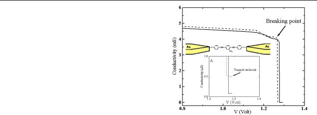
Figure 1. Conductivity–voltage plots of two junctions showing an initial gradual change in conductivity due to electromigration followed by an abrupt drop in current indicating that the junctions have been broken. Inset A: a zoom-in on the end of the two conductivity–V curves. The dashed curve shows a junction in which at least one molecule is bridging the gap between the Au leads (category (iii)). The lower curve corresponds to category (i). Only the dashed curve shows the temperature dependent behaviour discussed in the text.
voltage across the wires until a sudden drop occurred in their conductivity (see figure 1). The resulting current at this point is governed by tunnelling across the gap. Three types of behaviour can categorize all of the junctions following electromigration:
(i)Junctions with background level current that do not show
the temperature dependent behaviour described below. The resulting gaps are assumed to be larger than 3 nm and hence are not bridged by a molecule.
(ii)Junctions with currents orders of magnitude higher than the currents in figure 1 that do not show temperature dependent behaviour, and likely have either a small gap between the Au leads that allows direct tunnelling (not through a molecule) or a metal filament between the leads.
(iii)Junctions with intermediate current and the temperature behaviour seen in figures 2–5, which are regarded here as molecular junctions.
When no molecules were assembled on junctions prior to electromigration, they behaved either as in category (i) or (ii). All temperature dependent measurements were in the range 10–300 K.
3. Results and discussion
Molecule 1 was chosen for this study as a representative conjugated π system ‘molecular wire’. In addition, understanding charge transport in this molecule is important to elucidate the basis for its negative differential resistance (NDR) and memory properties [37–40].
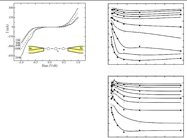
Figure 2 shows a representative set of current–voltage (I– V ) characteristics measured at temperatures between 13 and 200 K. It is essential to limit the measurements to a ±1 V window because voltages exceeding this range typically cause
S484
Temperature effects on conduction through a molecular junction
Figure 2. A set of I –V curves measured with molecule 1 chemisorbed in the junction at different temperatures (only a few representative temperatures are shown here for clarity).
degradation of the junction, which is probably due to excessive heat dissipation [41]. The values of current measured at 300 and 30 K at ±1 V are comparable to those of other single molecule junctions with similar molecular structure [24, 27]. The asymmetry of the I–V curves also indicates that a single molecule is trapped in this junction because the molecule is not symmetric. Alternatively, a small ensemble of molecules could be bridging the gap, with all its members oriented in the same direction.
The temperature dependent I–V characteristics of these junctions suggest that charge transfer through this molecule cannot be fully explained by McConnell’s superexchange mechanism [18]. According to this mechanism, the tunnelling rate through a bridge of arbitrary length, with N sites is proportional to:
N |
|
V |
|
2 |
|
n,n−1 |
|
|
|
McConnell rate |
|
|
|
(1) |
E |
||||
= |
|
|
|
|
|
|
|
|
|
n 1
where E is the energy gap between the Fermi level and the series of molecular levels 1, 2, . . . , N, all coupled in a tight binding fashion between nearest neighbours by an electronic coupling of magnitude V . The coupling V in this molecule is proportional to cos[θ ], where θ is the dihedral angle between rings [42]. At low temperature, θ = 0 (i.e. all rings are coplanar) since in this configuration the molecule gains maximum conjugation and stability. V is maximized in this configuration. As temperature increases, the rings start to fluctuate around their equilibrium position or even rotate freely (depending on the barrier for rotation, see discussion below). This results in a decrease of V [25] and an increase (in this specific molecule) of the HOMO–LUMO gap [43, 44]. If weak thermal coupling is assumed, which roughly corresponds to a situation where either E or the ‘bandwidth’ characterized by Vn,n−1 are much larger than level broadening due to thermal interactions, the McConnell rate should be temperature independent. In the strong thermal coupling limit, an overall decrease of the McConnell rate is expected according to equation (1). In either case, no increase in current is expected if superexchange as it is formulated in equation (1) is the
|
-15 |
|
|
|
|
|
-18 |
|
|
|
|
Ln(I) |
-21 |
|
|
|
|
|
|
|
|
|
|
|
-24 |
|
|
|
|
|
-27 |
|
|
|
|
|
0.00 |
0.02 |
0.04 |
0.06 |
0.08 |
|
|
|
1/T (1/K) |
|
|
|
-15 |
|
|
|
|
|
-18 |
|
|
|
|
Ln(I) |
-21 |
|
|
|
|
|
|
|
|
|
|
|
-24 |
|
|
|
|
|
-27 |
0.02 |
0.04 |
0.06 |
0.08 |
|
0.00 |
||||
|
|
|
1/T (1/K) |
|
|
Figure 3. Arrhenius plots of the current through two representative junctions showing a transition between coherent tunnelling at low temperature to a thermally activated incoherent hopping conduction at high temperature. In each plot a set of curves is presented for bias values between 0.1 V (lower curve) to 1.0 V (upper curve) with bias steps of 0.1 V. The bottom junction reveals a change of sign in the thermal activation slope at high temperatures (see text for details).
only conduction mechanism4. In contrast, however, an overall increase in current is observed in our junctions, which suggests that a thermally activated conduction mechanism operates in parallel with the superexchange mechanism.
Arrhenius plots of two representative junctions are shown in figure 3 and demonstrate a clear transition between temperature independent and thermally activated transport regimes. The observed thermally activated behaviour corresponds well to prior theoretical works [13– 17] that predict molecular conduction to be the result of parallel contributions from coherent tunnelling and incoherent hopping mechanisms. This apparent change from coherent
4 We refer here to the superexchange mechanism by the formulation in equation (1). Electron–phonon coupling can lead to a transient decrease ofE in the superexchange regime. This could result in temperature dependent behaviour where electrons (or holes) are still tunnelling elastically and can be considered as tunnelling in the superexchange regime. This effect will be discussed in detail in a following paper, where a different experimental approach is used to reveal this effect and isolate it from other temperature dependent mechanisms. The focus in this paper is on inelastic processes, where ultimately thermal activation results in hopping.
S485

Y Selzer et al
Figure 4. A plot of (numerically calculated) differential conductance (δ I /δV ) of a typical junction as a function of bias voltage (V ) and temperature (T ).
superexchange being the dominant conduction mechanism at low temperature to thermally activated hopping at higher temperature is most evident in the low bias regime (i.e. applied bias voltage <0.5 V). It has been argued that close to resonance the overall conduction can no longer be represented as an additive combination of coherent and incoherent contributions [4, 10, 16, 17]. The transition is also expected to be less evident in the limit of weak thermal coupling [16, 17], which is expected to prevail in our case where a single molecule under vacuum is thermally connected to its surrounding only by its bonds to the metal leads.
The differential conductance (δ I/δV ) of a typical junction as a function of bias voltage (V ) and temperature (T ) is shown in figure 4. A low conductance region around zero bias is revealed at 150 K and widens as the temperature decreases. The differential conductance in the gap is weakly dependent on temperature and essentially has the same value below 100 K. At each temperature below 150 K the gap is bounded in both bias polarities by what we refer to as transition potentials, which are defined as the potentials at which a sharp increase in δ I/δV takes place followed by monotonic increase in δ I/δV as a function of V . As will be discussed below, we believe that these transition potentials approximate the points on the I–V curves where coherent tunnelling ceases to be the primary conduction mechanism and incoherent hopping begins to become effective and eventually dominant.
It is evident from figure 4 that the zero bias conductance increases with temperature, which is further evidence that a thermally activated conduction mechanism dominates transport in the high temperature regime (i.e. system temperature T > 200 K). An Arrhenius plot can be generated from the zero bias conductance data as shown in figure 5. The transition between two conduction mechanisms is more clearly evident in this figure. For the simple case, where the molecule has only one state located E above EF, the overall conductance for small bias and sufficiently low temperature can be expressed as [16, 17]:
|
I |
|
e2 |
Tel(EF) 1+(1− f (EF + E)) |
κ |
|
|
g(EF) = |
|
= |
|
|
e− E/ kT |
||
|
πh¯ |
|
|||||
|
|
|
|
(2) |
|||
Figure 5. Arrhenius plot of zero bias conductance calculated from five junctions. The apparent barrier for the activated regime is
E = 56 meV.
where is the potential drop across the bridge, Tel is the elastic transmission and is the imaginary part of the self energy associated with the interaction of the bridge state with the metal electrodes. The conductance in this equation has a coherent contribution that is temperature independent and an incoherent thermally activated contribution. As the temperature is increased, dephasing and energy level relaxation start to play an increasing role, resulting in the incoherent contribution dominating over the coherent one. According to equation (2), the slope in figure 5 should correspond to the energy barrier ( E) to inject charge into the bridge states where hopping takes place. For our junctions, we found an average barrier, E 56 meV, which is small when compared to previous calculations that suggest the HOMO–LUMO gap of this molecule should be greater than 2 eV, and the Fermi level is expected to reside close to the middle of the gap [45, 46]. However, experimental results suggest that E, as measured by photoelectron spectroscopy, in a monolayer of a closely related system is near 0.5 eV [47]. In either case, these values do not correspond to the low apparent barrier that is extracted from our system. In addition, at V > 2 E0, (i.e. at bias values where resonant tunnelling would have been expected if E was indeed half the HOMO–LUMO gap), E is still greater than zero, which also implies that it is not the barrier to inject charge into the molecule. Alternatively, since experimental data does not yet exist regarding the size of the HOMO–LUMO gap or the relative position of the Fermi level in this system, it is possible that the barrier extracted from the Arrehenius plot is actually an intramolecular one, namely, for hopping between adjacent rings [13–15]. In support, we note that E correlates well with theoretical calculations of the rotational barriers in this molecule, which are approximately 40–50 meV for the left ring (see figure 2) and 80–100 meV for the right ring [48, 49]. The steric hindrance due to the position of the NO2 group on the central ring causes the difference between the rotational barriers of the different rings.
At very low system temperatures, we assume that the molecule in the junction is in a coplanar ring conformation. As the temperature is increased, the rings will begin to fluctuate increasingly around the optimized zero value dihedral angles.
S486

Temperature effects on conduction through a molecular junction
Based on theoretically calculated barriers, fluctuations in the left ring (in figure 2) are expected to take place at lower temperatures. If we assume that once fluctuations in the rings occur, coherency is suppressed and hopping becomes effective, then the expected barrier in figure 5 should correspond to the lowest rotational barrier in the system (i.e. the barrier to rotate the left ring). As the temperature is increased, fluctuations in the right and central rings start to take place as well. This could ultimately lead to further decrease in the electronic coupling between hopping sites, resulting in an overall decrease of the current [49, 50]. Alternatively, such behaviour has been predicted to occur when the dephasing rate of the bridge in a donor–bridge–acceptor system becomes too high compared to the rate of charge injection into the bridge [13–15]. We have observed a decrease in current and change in the Arrhenius slope (see lower panel of figure 3) at high temperature and high bias in several of our junctions, which could be attributed to the introduction of a second hopping mechanism with a higher energy barrier.
In the discussion and analysis above it was assumed that the temperature of the molecular junction equals that of the surrounding system. However, when inelastic processes are combined with inefficient heat conduction away from the molecular junction, the effective junction temperature could be substantially higher than the surrounding system [51, 52]. Several theoretical studies have already addressed this issue of local heating at the atomic level for atomic-scale metallic constrictions [53–56] as well as for molecules [51, 52, 57] by means of energy release via scattering with phonons and vibrations. These studies show that only a fraction of the available energy is released by the transmitted electrons onto the molecules, while most of the power is dissipated in the macroscopic leads to the junction. More significantly, however, the maximum power dissipation per atom is found on the molecules due to the high flux of electrons going through the molecules. Exact calculation of the resulting temperature of the junction depends on the ability to accurately calculate heat conductance through and away from the molecules [52]. Experimental evidence of local heating in single molecules can be found in several scanning tunnelling microscope (STM) experiments, where vibrational excitation by inelastic tunnelling electrons induces motions and reactions of single adsorbed molecules [58].
In the following discussion, we use a very simple model that does not explicitly account for heat conduction away from the junction to establish that the effective temperature of our molecular junctions is different from that of the surrounding system. The results also demonstrate the implications of the effective junction temperature on the initiation of the thermally activated hopping conduction mechanism. While we are aware that this model cannot be used to predict the absolute values of effective junction temperature, we believe that it qualitatively accounts for the effect of inelastic tunnelling and dissipation at low bias on the junction temperature.
For small currents in steady state there is a balance between excitation (due to inelastic tunnelling) and relaxation, which for a vibration ω yields a vibrational temperature Tvib which can be described by [59]:
kTvib = |
|
hω |
|
(3) |
ln |
( I/e) Pin+γ |
|
||
|
|
|
||
|
( I/e) Pin+γ e−hω/ kTb |
|||
where I is the current, Pin is the inelastic tunnelling fraction, γ is the inverse of the lifetime of the ν = 1 level, and Tb is the bath (surrounding system) temperature. By taking the currents at the transition potentials (from figure 4), using τ = 2 ps and Pin = 2×10⁻⁴ (see estimated probability in [8]), and assuming an average vibrational energy, ω, of 0.137 eV (calculated from the density of vibrational states of the molecule), we find a vibrational temperature of 100 K at all transition potentials below 100 K. This suggests that once the junction is above a certain effective temperature threshold, there is enough thermal energy inside the molecule to induce incoherency and dephasing, which ultimately decreases the probability for tunnelling and increases the probability for other modes of conductance, such as hopping. With increasing system temperature, fewer inelastic processes are needed in order to excite the molecule, and as a result the transition potentials are shifted to lower values. Once the system temperature is above the threshold (for this junction 100 K, see figures 3 and 4), activated processes will dominate molecular conduction even at zero bias5.
The expression for the effective vibrational temperature given in equation (3) can be simplified further when typical values of the free variables γ and Pin are considered. This simplified expression is given by:
kTvib |
|
|
hω |
|
. |
(4) |
|
γ |
|
||||
|
= ln |
|
|
|
|
|
|
( I/e) Pin |
|
|
|||
From this it can be seen that Tvib depends only weakly on γ , I and Pin, and strongly on the average vibrational energy, ω. Thus, the effective temperature 100 K is specific to this molecule through its average vibrational energy, and it does not depend on the exact value of the other variables. Once again, we note that the effective junction temperature of 100 K determined using this expression does not account for heat transfer away from the junction and probably does not reflect the actual junction temperature.
4. Conclusions and future work
The effect of temperature on conduction through a molecular junction formed from molecule 1 has been studied. Qualitative and semi-quantitative agreement with theory has been observed. Open issues regarding the observed activation energy of the thermal conduction process, as well as the difference between the effective temperatures of the junction and of the surrounding system have been discussed. These results further suggest that the exact temperature dependent conduction behaviour of a given molecular junction will
5 It can be shown from equation (3) that Tvib ≈ Tb for Tb > 100 K, which suggests that heating by inelastic effects is limited and determined by the vibrational modes that can be effectively excited by the tunnelling charge (ω). Once this limit is approached, the temperature of the molecule(s) will be equal to that of the surrounding system. This is consistent with the fact that relaxation increases with increasing temperature. It is also important for determining the hopping barrier since the barrier is extracted from the Arrhenius plot in a temperature range in which Tvib = Tb such that no correction to the slope is needed. It should also be noted that regardless of the formulation used to describe the temperature of the molecule as a result of heat dissipation, the correction in temperature required to change the barrier extracted from the slope of the Arrhenius plot even by a factor of two or three will make Tb unrealistic.
S487

Y Selzer et al
depend critically on the specific molecular structure, in particular the rotational barriers between adjacent rings and conduction units. Such structural correlation studies are now underway in our laboratories and should elucidate further important details of the fundamental conduction mechanisms.
Acknowledgments
Financial support was provided by the Defense Advanced Research Project Agency/Office of Naval Research (MC, TM, DA) and the Air Force Office of Scientific Research (YS, DA). We wish to thank Professors J Tour and Y Yao from Rice University for generously supplying samples of molecule 1. We acknowledge use of the electron-beam lithography system at the Penn State Nanofabrication Facility, which is funded by the NSF National Nanotechnology Infrastructure Network.
References
[1]Joachim C, Gimzewski J K and Aviram A 2000 Nature 408 541
[2]Heath J R, Kuekes P J, Snider G S and Williams R S 1998
Science 280 1716
[3]Okada A, Chernyak V and Mukamel S 1998 J. Phys. Chem. A 102 1241
[4]Petrov E G, Shevchenko Y V, Teslenko V I and May V 2001
J. Chem. Phys. 115 7107
[5]Davis W B, Ratner M A and Wasielewski M R 2001 J. Am. Chem. Soc. 123 7877
[6]Jortner J, Bixon M, Langenbacher T and
Michel-Beyerle M E 1998 Proc. Natl Acad. Sci. USA 95
12759
[7]Lambert C, Noll G and Schelter J 2002 Nat. Mater. 1 69
[8]Bade L, Petrov E G and May V 2003 Eur. Phys. J. D 26 187
[9]Pourtois G, Beljonne D, Cornil J, Ratner M A and
Bredas J L 2002 J. Am. Chem. Soc. 124 4436
[10]Petrov E G, Shevchenko Y V, Teslenko V I and May V 2003
Chem. Phys. 288 269
[11]Nitzan A 2001 J. Phys. Chem. A 105 2677
[12]Nitzan A 2002 Isr. J. Chem. 42 163
[13]Segal D, Nitzan A, Ratner M and Davis W B 2002 J. Phys. Chem. B 104 2790
[14]Segal D, Nitzan A, Davis W B, Wasielewski M R and Ratner M A 2000 J. Phys. Chem. B 104 3817
[15]Davis W B, Wasielewski M R, Ratner M A, Mujica V and Nitzan A 1997 J. Phys. Chem. A 101 6158
[16]Segal D and Nitzan A 2001 Chem. Phys. 268 315
[17]Segal D and Nitzan A 2002 Chem. Phys. 281 235
[18]McConnell H M 1961 J. Chem. Phys. 35 508
[19]Sikes H D, Smalley J F, Dudek S P, Cook A R, Newton M D, Chidsey C E D and Feldberg S W 2001 Science 291 1519
[20]Park H, Park J, Lim A K L, Anderson E H, Alivisatos P A and Mceuen P L 2000 Nature 407 57
[21]Park J et al 2002 Nature 417 722
[22]Liang W, Shores M P, Bockrath M, Long J R and Park H 2002
Nature 417 725
[23]Reed M A, Zhou C, Muller C J, Burgin T P and Tour J M 1997
Science 278 252
[24]Reichert J, Ochs R, Beckmann D, Weber H B, Mayor M and von Lohneysen H 2002 Phys. Rev. Lett. 88 176804
[25]Cui X D, Primak A, Zarate X, Tomfohr J, Sankey O F,
Moore A L, Moore T A, Gust D, Harris G and
Lindsay S M 2001 Science 294 571
[26] Smit R H M, Noat Y, Untiedt C, Lang N D,
van Hemert M C and van Ruitenbeek J M 2002 Nature
419906
[27]Reichert J, Weber H B, Mayor M and Lohneysen H v 2003
Appl. Phys. Lett. 82 4137
[28]Yu L H and Natelson D 2004 Nano Lett. 4 79
[29]Selzer Y, Cabassi M A, Mayer T S and Allara D L 2004 J. Am. Chem. Soc. 126 4052
[30]Wang W Y, Lee T and Reed M A 2003 Phys. Rev. B 68 035416
[31]Wang W Y, Lee T and Reed M A 2003 Physica E 19 117
[32]Zhou C, Deshpande M R, Reed M A, Jones L and
Tour J M 1997 Appl. Phys. Lett. 71 611
[33]Chen J, Calvet L C, Reed M A, Carr D W, Grubisha D S and Bennett D W 1999 Chem. Phys. Lett. 313 741
[34]Schull T L, Kushmerick J G, Patterson C H, George C, Moore M H, Pollack S K and Shashidhar R 2003 J. Am. Chem. Soc. 125 3202
[35]Kushmerick J G, Holt D B, Pollack S K, Ratner M A,
Yang J C, Schull T L, Naciri J, Moore M H and
Shashidhar R 2002 J. Am. Chem. Soc. 124 10654
[36]Kushmerick J G, Holt D B, Yang J C, Naciri J, Moore M H and Shashidhar R 2002 Phys. Rev. Lett. 89 86802
[37]Chen J, Reed M A, Rawlett A M and Tour J M 1999 Science 286 1550
[38]Rawlett A M, Hopson T J, Nagahara L A, Tsui R K, Ramachandran G K and Lindsay S M 2002 Appl. Phys. Lett. 81 3043
[39]Rawlett A M, Nagahara L A and Tsui R K 2002 Appl. Phys. Lett. 80 2761
[40]Stapleton J J, Harder P, Daniel T, Reinard M D, Yao Y,
Price D W, Tour J M and Allara D L 2003 Langmuir 19 8245
[41]Segal D and Nitzan A 2002 J. Chem. Phys. 117 3915
[42]Sachs S B, Dudek S P, Hsung R P, Sita L R, Smalley J F, Newton M D, Feldberg S W and Chidsey C E D 1997
J. Am. Chem. Soc. 119 10563
[43]Seminario J M and Derosa P A 2001 J. Am. Chem. Soc. 123 12418
[44]Derosa P A, Guda S and Seminario J M 2003 J. Am. Chem. Soc. 125 14240
[45]Taylor J, Brandbyge M and Stokbro K 2002 Phys. Rev. B 68 121101
[46]Taylor J, Brandbyge M and Stokbro K 2002 Phys. Rev. Lett. 89 138301
[47]Sikes H D, Sun Y, Dudek S P, Chidsey C E D and
Pianetta P 2003 J. Phys. Chem. B 107 1170
[48]Bauschlicher C W and Ricca A 2003 Chem. Phys. Lett. 375 459
[49]Majumder C, Briere T, Mizuseki H and Kawazoe Y 2002
J. Phys. Chem. A 106 7911
[50]Berlin Y A, Hutchison G R, Rempala P, Ratner M A and Michl J 2003 J. Phys. Chem. 107 3970
[51]Segal D and Nitzan A 2002 J. Chem. Phys. 117 3915
[52]Segal D, Nitzan A and Hanggi P 2003 J. Chem. Phys. 119 6840
[53]Todorov T N 1998 Phil. Mag. B 77 965
[54]Todorov T N, Hoekstra J and Sutton A P 2001 Phys. Rev. Lett. 86 3606
[55]Montgomery M J, Hoekstra J, Todorov T N and
Sutton A P 2003 J. Phys.: Condens. Matter 15 731
[56]Montgomery M J, Todorov T N and Sutton A P 2002 J. Phys.: Condens. Matter 14 5377
[57]Chen Y-C, Zwolak M and Di Ventra M 2003 Nano Lett. 3 1691
[58]Ueba H 2003 Surf. Rev. Lett. 10 771
[59]Walkup R E, Newns D M and Avouris Ph 1993 J. Electron. Spectrosc. 64/65 523
S488