

nanotechnology / jjap.ipap.44(1599)05pdf
.pdfJapanese Journal of Applied Physics Vol. 44, No. 4A, 2005, pp. 1599–1602
#2005 The Japan Society of Applied Physics
SELECTED TOPICS in APPLIED PHYSICS I
New Advances in Carbon Nanotube:
From New Growth Processes to Nanodevices
E ects of Fabrication Process on Current–Voltage Characteristics of Carbon Nanotube Field E ect Transistors
Takashi MIZUTANI , Shinya IWATSUKI, Yutaka OHNO and Shigeru KISHIMOTO
Department of Quantum Engineering, Nagoya University, Furo-cho, Chikusa-ku, Nagoya 464-8603, Japan
(Received October 6, 2004; revised November 15, 2004; accepted November 29, 2004; published April 8, 2005)
The e ects of the fabrication process on the current–voltage (I–V) characteristics of carbon nanotube field e ect transistors (CNT-FETs) were studied in detail. A large hysteresis observed in the I–V characteristics of the CNT-FETs having no passivation film became small by passivating the device surface with a SiNx film. The conduction behaivior of the CNT-FETs changed from p-type to ambipolar characteristics by SiNx passivation. Ambipolar characteristics were also observed in the top-gate CNT-FETs with a gate-source spacing of 2 mm. [DOI: 10.1143/JJAP.44.1599]
KEYWORDS: carbon nanotube, field effect transistor, hysteresis, ambipolar characteristics, SiNx , backgate, top gate
1.Introduction
Carbon nanotubes (CNTs) receive considerable attention from both physics and technological points of view because of their ideal one-dimensional structure, nanosize dimension, and high-current driving capability.1–3) One of the most useful applications of CNTs is in ultra high-density integrated circuits (ICs), which are expected to make a breakthrough in the limit of present silicon IC technology. Recently, Bachtold et al. have first demonstrated CNT IC; a ring oscillator consisting of three-stage CNT field-e ect transistor (FET) inverters.4) Even though their results are quite promising, the fabrication technique using CNTs dropped on a substrate is primitive. The position-controlled growth of CNTs is one of the most important technologies for the development of the fabrication process.
We have recently succeeded in fabricating CNT-FETs on a specified position by position-controlled CNT growth.5) By this technique, it is possible to evaluate the yields of CNTFETs. However, a fabricated device structure using a pþ- substrate as a back gate is not suitable for future device integration because input gate terminals are common to each other in back-gate CNT-FETs. Even though a top-gate device structure can eliminate the problem of the commongate configuration, additional processes such as gate insulator film deposition, and etching are required.
In this paper, we studied the e ects of the fabrication process on the current–voltage (I–V) characteristics of CNTFETs. The e ects of SiNx deposition and the subsequent top-gate process were studied. The hysteresis of the I–V characteristics and ambipolar behavior of the device were also examined.
2.Experiments
Figure 1(a) shows the schematic of the device structure. Position-controlled nanotube growth5) on a heavily doped pþ-Si substrate with thermally oxidized SiO2 (100 nm) was used as a wafer for device fabrication. First, metal catalysts consisting of a double layer of Co (2 nm) on Pt (10 nm) were patterned on the substrate using conventional photolithography and metal lift-o processes. An SEM image of the patterned catalysts is shown in Fig. 1(b). The gap between
E-mail address: tmizu@ieee.org
(a) |
Source |
CNT |
Drain |
|
|
Catalyst |
Catalyst |
Au/Ti |
|
|
|
|||
|
|
|
|
SiO2 |
|
|
Gate |
|
(100 nm) |
|
|
|
+ |
|
|
|
|
|
p –Si sub. |
|
|
|
|
Ti/Au |
(b)
Source Drain
Gap
100 m
Fig. 1. Schematic device structure (a) and patterned metal catalysts (b).
the catalysts for the source and drain electrodes and their width were 5 and 25 mm, respectively. Next, CNTs were synthesized by low-pressure thermal CVD. A mixture of ethanol and argon was used as a source gas. The flow rates were controlled with mass-flow controllers to be 50 and 100 sccm for ethanol and argon, respectively. The total pressure in the furnace was maintained at 2 Torr during the growth. According to Maruyama,6) alcohol is suitable for synthesizing SWNTs, which is probably because decomposed OH radical suppresses the generation of amorphous carbon. The growth temperature and duration were 900 C and 1 h, respectively. The fabrication was completed by Au/ Ti electrode formation both on the patterned catalysts and on the back surface of the substrate. The pþ-Si substrate was used as a gate electrode. The drain current–voltage (ID–VDS) characteristics of the fabricated CNT-FETs were measured in air. Little di erence in the ID–VDS characteristics was observed even when the device was measured in vacuum.
1599
1600 |
Jpn. J. Appl. Phys., Vol. 44, No. 4A (2005) |
T. MIZUTANI et al. |
|
|
|
|
0 |
|
|
|
|
|
|
|
|
|
|
|
|
|
|
|
|
|
|
|
|
|
|
|
|
-0.5 |
|
|
|
|
|
|
|
|
|
|
|
|
|
|
|
|
|
|
|
|
|
|
|
||
[ A] |
-1 |
|
|
|
|
|
|
|
|
|
|
|
|
|
|
|
|
|
|
|
|
|
|
||
D |
|
|
|
|
|
|
|
|
|
|
|
|
I |
|
|
|
|
|
|
|
|
|
|
|
|
-1.5 |
|
|
|
|
|
|
|
|
|
|
|
|
|
|
|
|
VBGS= -10~0 V: 1 Vstep |
|
|||||||
|
|
|
|
|
|
|
||||||
|
-2 |
|
|
|
|
|
|
|
|
|
|
|
|
|
|
|
|
|
|
|
|
|
|
||
|
|
|
|
|
|
|
|
|
|
|
|
|
|
-1 |
-0.8 |
-0.6 |
-0.4 |
-0.2 |
0 |
||||||
|
|
|
|
|
|
VDS [V] |
|
|
|
|
||
Fig. 2. ID–VDS characteristics of fabricated CNT-FET at room temperature.
Figure 2 shows the ID–VDS characteristics of a fabricated CNT-FET at room temperature. Here, gate voltage (VGS) is changed from 10 to 0 V in 1 V steps. ID increases with VGS toward the negative direction, indicating that the carriers in the channel are holes. Good pinch-o characteristics with a threshold voltage of 4 V were obtained. The maximum transconductance was 0.5 mS at VDS ¼ 1 V.
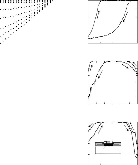
Figure 3(a) shows the ID–VGS characteristics of the fabricated CNT-FET. A large hysteresis was observed as shown in this figure. The direction of the hysteresis was clockwise. This indicates that the charge with an opposite sign against the gate voltage increased in the area of the gate during the gate bias. This means that the charge responsible for the hysteresis originates not from the gate electrode but from the channel or device surface, referring to the operation model of floating-gate memories of Si-MOSFETs.
We studied the e ect of passivation on the ID–VGS characteristics of the device. A SiNx passivation film with a thickness of 50 nm was deposited by two methods, namely ECR sputtering and thermal CVD. In ECR sputtering, no drain current was obtained after SiNx deposition. This is probably due to damage induced during the SiNx deposition. This is in contrast to our recent result for AlGaN/GaN MISHEMTs with a SiNx gate insulator deposited by ECR sputtering. The HEMTs showed good I–V characteristics with no surface-state-related transient signals.7) These results indicate that the CNT-FETs are very sensitive to surface damage, which might be induced in the CNT channel during the SiNx deposition. This is probably due to a large surface- to-volume ratio of the CNT channel. Good ID–VGS characteristics were obtained by thermal CVD.
Figure 3(b) shows the ID–VGS characteristics of the device passivated with a SiNx film deposited by thermal CVD at 250 C using a mixture of N2, NH3 and SiH4 as a source gas. Even though the direction of the hysteresis does not change, the amount of the hysteresis decreased. This indicates that the charge responsible for the hysteresis originates mainly not from the channel but from the surface of the device. The surface charge is presumed to be reduced by the SiNx passivation. According to Kim et al.,8) the most plausible origin of the surface charge is surface-adsorbed water molecules. We can expect the desorption of the water
|
0 |
|
|
|
|
|
|
|
-0.5 |
|
|
|
|
|
|
A] |
-1 |
|
|
|
|
|
|
|
|
|
|
|
|
|
|
[ |
|
|
|
|
|
|
|
D |
|
|
|
|
|
|
|
I |
-1.5 |
|
|
|
|
|
|
|
|
|
|
|
|
|
|
|
-2 |
|
|
|
|
|
|
|
-2.5 |
|
|
|
|
VDS= -1 V |
|
|
|
-5 |
0 |
|
5 |
10 |
|
|
-10 |
|
|
||||
|
|
|
|
VBGS [V] |
|
|
|
|
|
|
|
(a) |
|
|
|
|
0 |
|
|
|
|
|
|
-100 |
|
|
|
|
|
|
|
-200 |
|
|
|
|
|
|
|
[nA] -300 |
|
|
|
|
|
|
|
D |
|
|
|
|
|
|
|
I |
|
|
|
|
|
|
|
-400 |
|
|
|
|
|
|
|
-500 |
|
|
|
|
VDS= -1 V |
|
|
|
|
|
|
|
|
|
|
-600 |
-5 |
0 |
5 |
10 |
15 |
20 |
|
|
-10 |
||||||
|
|
|
|
VBGS [V] |
|
|
|
|
|
|
(b) |
|
|
|
0 |
|
|
|
|
|
-50 |
|
|
|
|
[nA] |
|
2 m |
Gate SiNx (50 nm) |
|
|
-100 |
Source |
Drain |
|
|
|
|
|
Au/ Ti |
|
||
D |
|
|
SiO |
|
|
I |
|
|
|
|
|
|
|
|
|
2 |
|
|
|
CNT |
p+-Si sub. |
|
|
|
-150 |
|
|
Au/ Ti |
|
|
Back Gate |
|
|
||
|
|
|
|
||
|
-200 |
|
|
VTGS= -1 V |
|
|
-5 |
0 |
5 |
10 |
|
|
-10 |
||||
|
|
|
VTGS [V] |
|
|
(c)
Fig. 3. ID–VGS characteristics of fabricated CNT-FET. (a) back-gate CNT-FET having no passivation film, (b) back-gate CNT-FET passivated with SiNx film deposited by thermal CVD, and (c) top-gate CNT-FET.
molecules during the SiNx deposition at 250 C. Moreover, the SiNx surface has few OH groups in contrast to the SiO2 surface, which results in fewer water molecules hydrogenbonded to the OH groups.
It is notable that the CNT-FET with the SiNx passivation film showed ambipolar characteristics with both n- and p- type conductions, as shown in Fig. 3(b). That is, starting from a negative gate voltage VGS from 10 V to 8 V, the current ID decreased towards 0 nA (p-channel), remained constant at 0 nA (o -state) for gate voltages between 8 V

Jpn. J. Appl. Phys., Vol. 44, No. 4A (2005) |
T. MIZUTANI et al. |
1601 |
|
|
|
and 9 V, and then gradually increased (n-channel). This indicates that the CNT-FET changed its conduction behavior from the p-channel to ambipolar characteristics by passivating the device surface with a SiNx film. Such ambipolar behavior has already been reported in some CNT-FETs9) and peapod FETs.10) Martel et al.9) explained it on the basis of the Schottky-barrier-controlled transistor model,11) in which the transistor action occurs primarily as a result of the change in Schottky-contact resistance induced by gate voltage rather than that in channel resistance. However they also analyzed Schottky barrier height based on its VDS dependence, which implicitly assumed that barrier height was controlled by drain voltage. However, this is not consistent with the previously proposed Schottky barrier control mode. We presume that Schottky barrier height is mainly controlled by gate voltage.
Figure 4 shows the energy band diagram of CNT-FETs, which show ambipolar characteristics. Figures 4(a)–4(d) correspond to the bias conditions at (a) zero bias, (b) p- type conduction, (c) o -state, and (d) n-type conduction, respectively. When negative voltage is applied to the gate electrode, the energy level of the CNT under the gate
source |
EC |
drain |
||||||
ΦBn |
|
|
|
|
|
|
|
|
|
|
|
|
|||||
|
|
|
|
|
|
|||
EF |
|
|
|
|
|
|
|
|
|
|
|
|
|
EV |
|
|
|
Φ |
|
|
|
|
|
|
|
|
|
|
|
|
|
|
|
||
Bp |
|
|
|
|
|
|
|
|
|
|
|
|
|
|
|
|
|
|
|
|
|
|
|
(a) |
|
|
VDS
hole
(b)l
(c) electron
(d)
Fig. 4. Energy band diagram of CNT-FETs at various bias conditions: (a) zero bias, (b) p-type conduction, (c) o -state, and (d) n-type conduction. The inset of Fig. 3(c) shows a schematic cross section of top-gate CNTFETs.
electrode shifts upward and holes are injected from the source electrode to the valence band, as shown in Fig. 4(b). When the gate voltage increases, the energy level of the CNT shifts downward. Then, the fermi level of the source electrode coincides with the energy gap of the CNT, as shown in Fig. 4(c). In this case, hole injection from the source electrode to the CNT channel is inhibited, which corresponds to the o -state of the CNT-FETs. When the gate voltage increases further, the energy level further shifts downward, as shown in Fig. 4(d). In this case, even though the hole injection from the source electrode is still inhibited, electron injection from the contact electrode on the opposite side occurs, which corresponds to the n-type conduction. In this current control model, it is easy to observe the ambipolar characteristics of the device with a small-bandgap CNT channel, and those of the device where the Fermi level of the contact electrodes is near the mid gap. The gate voltage width for the o -state reflects the bandgap of the CNT channel. In such a type of model, it will be possible to implement n-channel CNT-FETs using a contact metal with a small work function. This has been demonstrated recently using Ca as a small-work-function electrode.12)
It is worth discussing the reason the conduction behavior changes from p-type to an ambipolar characteristic following the passivation of the device surface. One of the possible reasons is that the position of the Fermi level of the source/ drain contact metal shifts toward the mid gap of the CNT channel. In this case, even though the Schottky barrier height against hole injection slightly increases, the barrier height against electron injection decreases. Therefore, it is easier to inject electrons from the electrode on the opposite side, which leads to an ambipolar characteristic with a decrease in drain current in the p-type conduction regime. This is consistent with the experimental result shown in Fig. 3(b), where CNT-FET shows ambipolar characteristics with a smaller drain current in the p-type conduction region than that in Fig. 3(a).
Concerning the origin of Fermi level shift, it has been reported that the dipole is formed at the interface between the CNT and the contact electrode, and that the amount of dipole is dependent on oxygen adsorption.9) The interface dipole field changes the position of the Fermi energy at the contact metal/CNT interface. These phenomena might occur at the electrode edge during SiNx deposition. Another possible explanation is the e ect of strain caused by the SiNx film. If bandgap decreases due to strain, it is also easy to realize ambipolar characteristics. According to the calculation by Yang and Han,13) the band gap changes under strain, and the direction of the change is dependent on chirality. Quantitative discussion will be conducted in future studies.
It is interesting to study whether these ambipolar characteristics occur in top-gate CNT-FETs or not, where a gap exists between the gate and source electrodes. This is because modulation of Schottky barrier thickness at the contact by the gate is dependent on the gap distance. The schematic cross section of top-gate CNT-FETs is shown in the inset of Fig. 3(c). A top-gate electrode was formed on the SiNx passivation film with a 50 nm thickness. The gatesource distance was 2 mm. Figure 3(c) shows the ID–VGS characteristics of the top gate CNT-FET. It is notable that
I HYSICSP PPLIEDA in OPICST ELECTEDS
1602 |
Jpn. J. Appl. Phys., Vol. 44, No. 4A (2005) |
T. MIZUTANI et al. |
|
|
|
ambipolar characteristics were observed even in the top gate CNT-FET with a long gate-source distance of 2 mm. According to the calculation by Leonard and Terso ,14) the full-depletion width, which is a measure of the distance where modulation of Schottky barrier thickness by the gate occurs, can even be in one micron at doping fraction (the number of dopants per atom) of approximately 2 10 4. Our experimental results suggest that the doping fraction of the CNT channel is at around this level.
It is notable that the direction of hysteresis of the present top-gate FETs is opposite to that of the back-gate FETs in the p-type conduction regime. That is, it was counterclockwise for the top-gate FET and clockwise for the back-gate FET. Counterclockwise hysteresis indicates that the charge responsible for the hysteresis originates from the gate electrode. For top-gate FETs, thinner SiNx (50 nm) with a smaller conduction band o set (approximately 2.5 eV) than those of a SiO2 back-gate insulator (100 nm, approximately 3.7 eV) was used. This might result in a tunneling injection of electrons from the gate to the SiNx gate insulator or the SiNx/CNT interface during negative gate bias. Further investigation is ongoing and relegated to future publication.
3.Summary
The e ects of fabrication process on the I–V characteristics of CNT-FETs were studied in detail. A large hysteresis was observed in the I–V characteristics of the back-gate CNT-FETs without a passivation film. The direction of the hysteresis was clockwise. The hysteresis became small by passivating a device surface with a SiNx film grown by thermal CVD. Water molecules adsorbed on the device surface were suggested as the origin of the hysteresis of the bare CNT-FETs on the basis of these results. The conduction behavior of the CNT-FETs has changed from p-type to ambipolar characteristics by passivating the device surface
with a SiNx film. Even in the top-gate CNT-FETs with a gate-source spacing of 2 mm, ambipolar characteristics were observed. Moreover, the direction of the hysteresis was di erent between the back-gate and the top-gate devices. This suggests that there are other causes of hysteresis in the I–V characteristics.
Acknowledgment
This work was supported in part by the Special Coordination Funds of the Ministry of Education, Culture, Sports, Science, and Technology of the Japanese Government.
1)C. Dekker: Phys. Today 52 (1999) 22.
2)M. S. Dresselhaus, G. Dresselhaus and P. C. Eklund: Science of Fullerenes and Carbon Nanotubes (Academic Press, New York, 1996).
3)M. S. Dresselhaus, G. Dresselhaus and P. Avouris: Carbon Nanotubes (Springer, Berlin, 2001) Springer Series Vol. 80.
4)A. Bachtold, P. Hadley, T. Nakanishi and C. Dekker: Science 294 (2001) 1317.
5)Y. Ohno, S. Iwatsuki, T. Hiraoka, T. Okazaki, S. Kishimoto, K. Maezawa, H. Shinohara and T. Mizutani: Jpn. J. Appl. Phys. 42 (2003) 4116.
6)S. Maruyama, R. Kojima, Y. Miyauchi, S. Chiashi and M. Kohno: Chem. Phys. Lett. 360 (2002) 229.
7)M. Ochiai, M. Akita, Y. Ohno, S. Kishimoto, K. Maezawa and
T.Mizutani: Jpn. J. Appl. Phys. 42 (2003) 2278.
8)W. Kim, A. Javey, O. Vermesh, Q. Wang, Y. Li and H. Dai: Nano Lett. 3 (2003) 193.
9)R. Martel, V. Derycke, C. Lavoie, J. Appenzeller, K. K. Chan,
J.Terso and Ph. Avouris: Phys. Rev. Lett. 87 (2001) 256805.
10)T. Shimada, T. Okazaki, R. Taniguchi, T. Sugai and H. Shinohara: Appl. Phys. Lett. 81 (2002) 4067.
11)S. Heinze, J. Terso , R. Martel, V. Derycke, J. Appenzeller and Ph. Avouris: Phys. Rev. Lett. 89 (2002) 106801.
12)Y. Nosho, Y. Ohno, S. Kishimoto and T. Mizutani: Appl. Phys. Lett. 86 (2005) 73105.
13)L. Yang and J. Han: Phys. Rev. Lett. 85 (2000) 154.
14)F. Leonard and J. Terso : Phys. Rev. Lett. 83 (1999) 5174.