

nanotechnology / NA2327
.PDFINSTITUTE OF PHYSICS PUBLISHING |
NANOTECHNOLOGY |
Nanotechnology 13 (2002) 378–381 |
PII: S0957-4484(02)31500-9 |
An ab initio approach to electrical transport in molecular devices
J J Palacios1, E Louis1, A J Perez´-Jimenez´2, E San Fabian´2 and
J A Verges´3
1Departamento de F´ısica Aplicada y Unidad Asociada UA-CSIC, Universidad de Alicante, San Vicente del Raspeig, Alicante 03080, Spain
2Departamento de Qu´ımica-F´ısica y Unidad Asociada UA-CSIC, Universidad de Alicante, San Vicente del Raspeig, Alicante 03080, Spain
3Instituto de Ciencia de Materiales de Madrid (CSIC), Cantoblanco, Madrid 28049, Spain
Received 4 December 2001, in final form 8 April 2002
Published 23 May 2002
Online at stacks.iop.org/Nano/13/378
Abstract
We present a theoretical study of scanning tunnelling microscopy of a C60 molecule adsorbed on Al and Au(111) surfaces and of electrical transport of short metallic nanotubes contacted in two ways to such surfaces. For the case of an adsorbed C60 molecule, the change of substrate metal is reflected in a different charge transfer, in a different alignment of the Fermi level with respect to the molecular orbitals and, consequently, in a very different zero-bias transparency. For the case of metallic nanotubes with realistic contacts, the conductance turns out to be, at best, half the ideal value of
4e2/h. We perform these studies within a recently developed ab initio scheme suitable for studying electrical transport in generic single-molecule junctions.
(Some figures in this article are in colour only in the electronic version)
1. Introduction
The simplest element in molecular electronic devices is the molecular bridge or single-molecule junction where a molecule acts as a bridge for current between two separate metallic leads. Among the large variety of molecules that can be used for this purpose, fullerenes and carbon nanotubes are expected to play a key role due to their peculiar and well known electronic and structural properties [1]. Recently, C60 molecules have been evaporated on gold break-junctions [2]. They also perform as a bridge in scanning tunnelling microscopy (STM) experiments in which the C60 molecules are adsorbed on different metallic substrates [3]. Here, the tip and the metallic substrate act as electrodes. Similarly, carbon nanotube electrical properties have been explored by contacting them to lithographically defined electrodes [1]. In all these cases the same electrode– molecule–electrode scheme is present.
The injection of current through these molecules is logically determined by their electronic structure. However, the metallic contacts do not only probe the electronic properties of the molecule, but often play an important role in the overall electrical performance of the device. Orbital hybridization and charge transfer processes are typically present, with the
consequent changes in the total charge and electronic structure of the molecule, hence the necessity of applying self-consistent or ab initio methods to the study of the electrical transport in these systems.
2. The Gaussian embedded cluster method (GECM)
In a previous work [4] we presented a method to study transport in generic molecular junctions which is based on standard quantum chemistry calculations using the Gaussian98 code [5]. The use of the Gaussian98 code for transport calculations, which is being adopted by other groups (see, e.g., [6]), is here taken a step further. A density functional (DF) calculation of the molecule with a significant part of the contacts attached is performed (see figure 1). The Hamiltonian (or Fock matrix
ˆ ) of the electrode–molecule–electrode system contains the
F
relevant information, but, according to the usual theoretical transport schemes [7], its associated Green functions are unsuitable for the evaluation of the current (note that they will simply have poles). The retarded (advanced) Green functions
associated with ˆ need to be transformed into the retarded
F
(advanced) Green function of an infinite system:
0957-4484/02/030378+04$30.00 © 2002 IOP Publishing Ltd Printed in the UK |
378 |
An ab initio approach to electrical transport in molecular devices
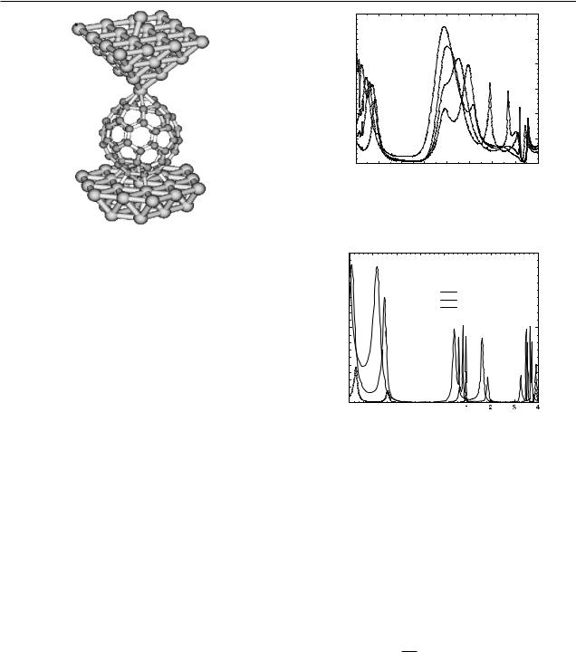
Figure 1. Schematic representation of a C60 molecule deposited on an Al(111) surface with a nearby tip of the same material.
ˆ |
= |
|
ˆ ˆ |
− ˆ ± |
iδ)−1 |
→ |
ˆ ˆ |
− ˆ |
− ˆ |
|
||
Gr(a)( ) |
|
( I S |
F |
|
|
[ I S |
F |
r(a)( )]−1. |
(1) |
|||
In this expression |
|
= ˆ R |
|
ˆ L |
|
|
||||||
|
|
|
ˆ |
|
|
|
|
|||||
|
|
|
r(a)( ) |
|
r(a)( ) + r(a)( ), |
(2) |
||||||
where |
|
) |
denotes a self-energy matrix that accounts for |
|||||||||
ˆ R ( ˆ L |
|
|||||||||||
the part of the right (left) infinite electrode which has not been
included in the DF calculation and ˆ is the overlap matrix. The
S
added self-energy matrices can only be explicitly calculated in ideal situations, which, in principle, might seem to limit the desired applicability of the above procedure. However, as pointed out by Landauer in his scattering description of electrical transport [7], the bulk details of a metallic electrode are not necessarily relevant for the electrical transport properties of the region with the smallest number of channels. We choose to describe the bulk electrode with a Bethe lattice tight-binding model with the appropriate coordination number and tight-binding parameters. The advantage of choosing a Bethe lattice resides in the fact that the self-energy matrices can be calculated iteratively in a simple way [8]. For each atom in the metallic electrodes of the cluster with a missing near-neighbour atom a contribution from an infinite Bethe lattice in the appropriate direction is added. Assuming that the most important structural details of the electrode are included in the cluster the Bethe lattice should introduce no spurious effects. This is the main difference with respect to other methods that have been developed recently [9] to calculate transport properties from first principles.
In our new approach the self-consistent process does not stop once the finite cluster has once been solved. Instead, we force the Gaussian98 code to proceed with the self-consistency of the now infinite system. More specifically, once selfconsistency for the finite cluster has been almost attained, we calculate the Green function as explained above. Then, the density matrix is obtained from the Green function according to
|
1 |
F |
|
|
|
ˆ = − |
Im [ ˆ |
] d |
|
|
|
|
|
|
|||
n |
|
Gr ( ) |
|
, |
(3) |
π −∞
where F is the Fermi level fixed by the condition of charge neutrality in the cluster. The density matrix is now used to calculate again the matrix elements of the Fock operator and the process
|
3 |
|
|
|
|
|
|
|
|
|
|
|
|
0.5 A |
|
|
|
|
|
|
2.5 |
|
|
|
1 A |
|
|
|
|
|
|
|
|
|
|
|
|
|
|
|
|
|
|
|
1.5 A |
|
|
|
|
|
2 |
|
|
|
|
|
|
|
|
/h) |
|
|
|
|
|
|
|
|
|
2 |
1.5 |
|
|
|
|
|
|
|
|
G (2e |
|
|
|
|
|
|
|
|
|
|
|
|
|
|
|
|
|
|
|
|
1 |
|
|
|
|
|
|
|
|
|
|
|
|
|
2 A |
|
|
|
|
|
0.5 |
|
|
|
|
|
|
|
|
|
0 |
–3 |
–2 |
–1 |
0 |
1 |
2 |
3 |
4 |
|
–4 |
||||||||
|
|
|
|
|
Energy (eV) |
|
|
|
|
Figure 2. Conductance around the Fermi energy (here set to zero) of a C60 molecule deposited on an Al(111) surface at equilibrium distance and contacted by a tip of the same material at several distances from the molecule.
2
d = 1.5A d = 2.5A d = 3.5A
/h) |
|
2 |
|
(2eG |
1 |
|
0 


 –4 –3 –2 –1 0
Energy (eV)
Figure 3. Conductance around the Fermi energy (here set to zero) of a C60 molecule deposited on a Au(111) surface at equilibrium distance and contacted by a tip of the same material at several distances from the molecule.
is repeated until self-consistency is achieved. The final Green function describes an infinite system in a more consistent way than in the method discussed previously [4]. It is interesting to note that the applicability of this approach, which we hereafter name the Gaussian embedded cluster method (GECM), goes well beyond the present study. In fact it could be a powerful tool whenever an infinite medium has to be described (for instance adsorption of molecules on solid or liquid surfaces).
The conductance can now be simply calculated through the expression [7]
|
2e2 |
|
G = |
h Tr[ LGr R Ga ], |
(4) |
where Tr denotes the trace over all the orbitals of the cluster and the matrices R and L are given by i( Rr − Ra ) and i( Lr − La ), respectively.
2.1. Scanning tunnelling microscopy of C60 molecules
We now apply the GECM to the study of STM of C60 molecules (see a schematic view in figure 1). In figures 2 and 3 we present results of G for C60 molecules adsorbed on Al(111) and Au(111) surfaces, using the same metal for both tip and substrate. In both cases the C60 molecule has been allowed to find the equilibrium distance on the surface. We see a clear
379
J J Palacios et al
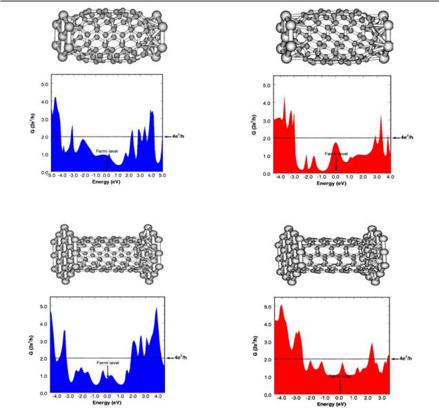
Figure 4. Conductance of a short (5, 5) capped nanotube in between two parallel Al(111) surfaces at a contact distance of 1 Å.
Figure 5. Conductance of a short (5, 5) nanotube in between two parallel Al(111) surfaces at a contact distance of 1 Å.
region of low (or even zero) conductance close to the Fermi energy (here set to zero). The origin of this reduced conductance lies in the HOMO–LUMO gap of the C60 molecule. There is, however, a fundamental difference between Al and Au. For Al the charge transfer from the surface to the molecule is larger than for Au (≈2 electrons for Al and ≈0.4 electrons for Au). This charge transfer situates the Fermi energy in the middle of the LUMOs for Al while it keeps it in the gap for Au (although very close to the LUMOs). This has a dramatic effect on the conductance since, while for Al the molecule turns out to be transparent at zero bias, the zero-bias current in the case of Au is always negligible. Here the molecule acts as a diode. In both cases we also present an analysis of the conductance with the distance of the tip from the molecule. The conductance increases as the molecule–tip distance decreases, but, in addition, the structure of the conductance changes due to the influence of the tip on the density of states of the adsorbed molecule. At large distances, i.e. in the tunnelling regime, the conduc-
Figure 6. Conductance of a short (5, 5) capped nanotube in between two parallel Au(111) surfaces at a contact distance of 1 Å.
Figure 7. Conductance of a short (5, 5) nanotube in between two parallel Au(111)surfaces at a contact distance of 1 Å.
tance only varies in magnitude, not in the overall structure.
2.2. Conductance of short metallic carbon nanotubes
We have employed the GECM to calculate the current in (5, 5) metallic nanotubes contacted symmetrically to Al(111) and Au(111) parallel surfaces. Two cases have been considered for each metal: capped and open nanotubes. Infinite metallic nanotubes have two bands crossing at the Fermi level and they are expected to present a conductance of 4e2/h over a range of energies of ≈2 eV around the Fermi level. For ideal (adiabatic) contacts to the electrodes this value should still hold. The results presented in figures 4–7 clearly indicate that this is not the case. The conductance barely reaches 2e2/h even for the cases of open nanotubes, where the number of atoms involved in the transmission is larger and the contact to the metal is expected to be better. No optimization of the contact distance has been performed, choosing 1 Å for all cases. This is not a realistic
380

An ab initio approach to electrical transport in molecular devices
distance and it is expected to be different for different types of metal, surface and nanotube-end geometries. In fact, a larger contact distance is expected in all the cases considered here and resonances due the presence of quasi-bound states should appear in the conductance [10]. We have taken this unrealistic value on purpose to illustrate the fact that even forcing a good contact is not enough to obtain the ideal value of 4e2/h.
In conclusion, we have developed a methodology to calculate ab initio transport properties in molecular systems based upon the Gaussian98 code. This opens the doors to the use of the most standard quantum chemistry tool in the study of transport through molecules. We have chosen to study two systems that illustrate the prediction capabilities of our approach: C60 molecules adsorbed on a reactive electrode (Al) and an ‘inert’ (Au) electrode and short nanotubes with realistic contacts.
Acknowledgments
This work was supported by the Spanish CICYT under grants nos 1FD97-1358 and PB96-0085, and by the Generalitat Valenciana under grant no GV00-151-01. Discussions with J C Sancho, L Pastor-Abia and J M Perez´-Jorda´ are acknowledged.
References
[1]For nice reviews on the issue see Dekker C 1999 Phys. Today 52 22
Joachim C, Gimzewski J K and Aviram A 2000 Nature 408 541
[2]Park H et al 2000 Nature 407 57
[3]Joachim C et al 1995 Phys. Rev. Lett. 74 2102 Porath D et al 1997 Phys. Rev. B 56 9829 Hou J G et al 1999 Phys. Rev. Lett. 83 3001
Pascual J I et al 2000 Chem. Phys. Lett. 321 78
[4]Palacios J J, Perez´-Jimenez´ A J, Louis E and Verges´ J A 2001
Phys. Rev. B 64 115411
[5]Gaussian 98 1998 (Pittsburgh, PA: Gaussian)
[6]Heurich J, Cuevas J C, Wenzel W and Schoen G 2001 Preprint arXiv cond-mat/0110147
[7]Datta S 1995 Electronic Transport in Mesoscopic Systems ed H Ahmed, M Pepper and A Broers (Cambridge: Cambridge University Press)
[8]Palacios J J, Perez´-Jimenez´ A J, Louis E, SanFabian´ E and Verges´ J A 2002 Preprint arXiv cond-mat/0202375
[9]Lang N D 1995 Phys. Rev. B 53 5335
Hirose K and Tsukada M 1995 Phys. Rev. B 51 5278 Taylor J, Guo H and Wang J 2001 Phys. Rev. B 63 245407
Brandbyge M, Taylor J, Stokbro K, Mozos J L and Ordejon´ P 2001 Preprint arXiv cond-mat/0110650
Yaliraki S N et al 1999 J. Chem. Phys. 111 6997 Xue Y, Datta S and Ratner M A 2001 Preprint arXiv
cond-mat/0112136
[10]Palacios J J and Perez´-Jimenez´ A J 2002 in preparation
381