

nanotechnology / apl98(84505)05
.pdfJOURNAL OF APPLIED PHYSICS 98, 084505 2005
Operation and properties of ambipolar organic field-effect transistors
G. Paascha and Th. Lindner
Leibniz Institute for Solid State and Materials Research (IFW) Dresden, PF 270116, 01171 Dresden, Germany
C. Rost-Bietsch,b S. Karg, and W. Riess
IBM Research GmbH, Zurich Research Laboratory, Säumerstrasse 4, 8893 Rüschlikon, Switzerland
S. Scheinertc
Ilmenau Technical University, Institute of Solid State Electronics, PF 100565, 98684 Ilmenau, Germany
Received 19 January 2005; accepted 30 August 2005; published online 19 October 2005
Two-dimensional simulations of ambipolar or double-injection Þeld-effect transistors FETs based on organic materials as active layer are presented in this article. These organic FETs are of interest because of the direct recombination accompanied by light emission. When modeling such FETs, one problem is that even advanced existing models based on the Pao-Sah description neglect both the actual contact properties and the recombination process. We present numerical simulations taking account these peculiarities. Current-voltage characteristics are used as reference data, recently obtained on an organic heterostructure ambipolar FET with a bottom Au contact and a Mg top contact Rost et al., J. Appl. Phys. 95 5872 2004 . To investigate the basic ambipolar effects without the additional inßuences of the special structure, a single-layer model structure is considered in this simulation study. Simulated current-voltage characteristics indeed feature all speciÞc characteristics arising from the ambipolar operation. Their origin becomes clear by inspecting the internal Þeld and concentration proÞles. The simulations reveal a complex interplay between the properties of the source and gate contacts, interface charges, the ratio of the electron and hole mobilities, doping, and recombination. Thereby, pronounced ambipolar operation depends sensitively on the combination of the barrier of the electron-injecting contact and the ratio of hole to electron mobilities. Possibilities and limitations of direct parameter extraction based on simple analytical expressions are demonstrated. © 2005 American Institute of Physics.
DOI: 10.1063/1.2085314
I. INTRODUCTION
Combining light-emission with switching characteristics in a single device, i.e., a light-emitting Þeld-effect transistorFET , would increase the number of potential applications of organic optoelectronic devices signiÞcantly. Light emission from a FET requires electron and hole injection and transport, the so-called ambipolar transport, as well as efÞcient radiative decay. Evidence of the ambipolar behavior of hydrogenated amorphous silicon a-Si:H thin-Þlm transistors TFTs was found almost 30 years ago by Neudeck and
Malhotra.1 Detailed investigations were presented a decade later by Pßeiderer et al.,2Ð5 Hack et al.,6 and Neudeck
et al..7,8 Hack et al. emphasized that one obtains much larger currents than in a conventional a-Si:H TFT, and proposed the possibility of visible-light-emitting transistors whose emission can be modulated at high speed. However, a-Si:H does not emit light efÞciently, and this new type of device did not Þnd applications. Recently, an ambipolar Schottky barrier silicon-on-insulator metal-oxide-semiconductorMOS transistor with promising electrical properties has been presented.9 In another recent article,10 ambipolar Þeld-
a Author to whom correspondence should be addressed; electronic mail: g.paasch@ifw-dresden.de; URL: www.ifw-dresden.de/~paasch/
b Electronic mail: cro@zurich.ibm.com c Electronic mail: susanne.scheinert@tu-ilmenau.de
effect carrier injections in organic insulators have been reported. Ambipolar transport characteristics have also been
observed in double-well carbon-nanotube FETs at low temperature 23 K .11
Organic low-molecular-weight materials and conjugated polymers are now successfully used as active materials in organic light-emitting diodes OLED for display applications.12,13 These materials usually are either electron or hole conductors, or they are unintentionally n or p doped. In order to achieve balanced electron and hole transport as well as efÞcient injection of both types of carriers for an ambipolar FET, various alternative approaches exist. One recent realization is based on an interpenetrating network of two materials.14 Dodabalapur et al. used -hexithienylene-6T and C60 as active layers, and identical Au electrodes as source and drain contacts.15 In their structure, symmetrical source and drain contacts lead to an injection barrier for at least one type of charge carriers. In this particular case, the choice of Au strongly limits electron injection. In a Þrst approach, we used an organic heterostructure FET optimized to achieve efÞcient hole and electron injection as well as p- and n-channel device operation.16 We reported an ambipolar heterostructure organic FET OFET that consisted of pentacene as hole-transport material and N, N -Ditride- cylperylene-3,4,9,10-tetracarboxylic diimide P13 as electron-transport material combined with optimized source
0021-8979/2005/98 8 /084505/13/$22.50 |
98, 084505-1 |
© 2005 American Institute of Physics |
Downloaded 27 Nov 2006 to 146.103.254.11. Redistribution subject to AIP license or copyright, see http://jap.aip.org/jap/copyright.jsp
084505-2 |
Paasch et al. |
J. Appl. Phys. 98, 084505 2005 |
and drain electrodes of Au and Mg, respectively. An ambipolar light-emitting OFET was demonstrated by replacing pentacene with a more suitable hole-transport material.17 Other groups have shown light-emitting OFETs based on single-layer tetracene; however, without any indication of ambipolar transport.18,19 Visible-light emission from a polymer-based poly 2-methoxy-5- 2-ethyl-hexyloxy -1,4- phenylene vinglene MEH-PPV FET at relatively high voltages is reported in Ref. 20. Here composite Al/Au electrodes have been used for both source and drain. Recently, in a structure similar to a static induction transistor that uses organic multilayers for light emission, a shift of the turn-on voltage and enhanced luminescence have been observed upon the application of a gate voltage.21 However, this device does not combine light emission with switching charac-
teristics.
Until now, the models for ambipolar TFTs2Ð5,7,8 have either been based on a modiÞed Pao-Sah22 description for unipolar FETs or on the graduate channel approximation. Thereby, a non-Ohmic nature of at least one of the contacts and recombination are not taken into account. But in the organic ambipolar TFTs, both contacts are decisive for the operation. Therefore, an adequate description of the behavior of such devices requires the use of state-of-the-art twodimensional 2D numerical simulations. In this article, we present a Þrst simulation study for a single-layer model system using the recent experimental data of the heterostructure device16 as reference. This leads to a proper understanding of the operation principles, clariÞes the decisive inßuence of the nature of the contacts, and the sensitivity to variations in the material parameters. Furthermore, the possibilities and restrictions of data analysis using simple analytical expressions are demonstrated.
In Sec. II we brießy review the properties of ambipolar TFTs as a basis for the simulations and summarize our experimental results.16 In Sec. III both the model and the simulation method are described and standard parameters given. Section IV presents and discusses the results whereas parameter extraction is analyzed in Sec. V. Conclusions are drawn in Sec. VI, where we also outline a subsequent article dealing with the heterolayer device.
II. PROPERTIES OF AMBIPOLAR FIELD-EFFECT TRANSISTORS
A. Device based on amorphous silicon
The most common TFTs based on a-Si:H operate as unipolar devices by forming either an n channel or a p channel. The operation in inversion or accumulation mode is controlled by the contacts chosen to be either rectifying or Ohmic, respectively. Another concept has been introduced by Pßeiderer et al.2Ð5 in which source and drain contacts are Ohmic for majority as well as minority carriers. These TFTs exhibit n-channel, p-channel, and ambipolar operation, depending on the applied gate-source and drain-source voltages, and have been studied in detail also in Refs. 6Ð8.
The main feature in the output characteristics of the ambipolar device is a strong increase of the drain current for large drain-source voltages in addition to the linear and satu-
ration regions. This can be understood as follows. For a
negative effective gate-source voltage VGS,eff, with VGS,eff =VGS −Vth 0, where VGS is the applied gate voltage and Vth
the threshold voltage, a hole accumulation layer is formed owing to hole injection at the source and drain contacts if these contacts are Ohmic for holes. The electron inversion
layer for VGS,eff 0 cannot be formed if these contacts are blocking for electrons. For small negative drain-source volt-
age VDS 0, the drain current ID is in the active or linear regime. Thereby the gate-drain voltage is effectively reduced
to VGD =VGS,eff −VDS. As VDS approaches VGS,eff the region close to the drain becomes depleted and ID saturates. For
even larger negative VDS, the condition for inversion is fulÞlled at the drain contact but the electron-blocking drain contact prevents this channel from being formed. Replacing this contact by one that is Ohmic for electrons2Ð5 leads to the electron inversion channel near the drain contact for −VDS
−VGS,eff, in addition to the hole channel near the source. The additional electron current leads to a strong increase of
the total drain current ID. If both source and drain are Ohmic for electrons and holes, the transfer characteristics do not consist of only an ÒonÓ and an ÒoffÓ regions, as it is known from unipolar device operation. Instead, Òon-off-onÓ states are observed for increasing gate voltages.
Proposed circuit applications of these devices that exploit the characteristics of ambipolar transport have not yet been realized. With hole injection at one contact and electron injection at the other, charge-carrier recombination becomes important for the operation. To combine switching with light emission due to radiative recombination as proposed in Ref. 6 requires the replacement of a-Si:H by a suitable emitter.
B. Organic heterostructure device with asymmetric source and drain contacts
In devices with organic semiconductors as active material, source and drain usually consist of metals. In this case an Ohmic or accumulation contact for one type of carrier inevitably is a Schottky contact for the other. Thus, in the organic heterostructure ambipolar FET described in Ref. 15, the electron channel yields a rather low current because gold was used for both source and drain. Our design aims at combining the bilayer heterostructure principle with the use of different metals for source and drain. The bilayer is formed from an electron-transport material and a hole-transport material. The two contact metals were chosen to provide efÞcient electron and hole injections.
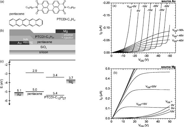
In the heterostructure OFET devices described, pentacene was used as the hole-transport material and N, N -Ditridecylperylene-3,4,9,10-tetracarboxylic diimideP13 as the electron-transport material. The molecular structures and the schematic architecture of this device are shown in Figs. 1 a and 1 b . Device preparation and measurement setup have been described in detail in Ref. 16. The channel length and width of the heterostructure OFET were 140 and 2000 m, respectively. The energetic levels of the highest occupied molecular orbital HOMO and the lowest unoccupied molecular orbital LUMO of pentacene and of P13 with respect to the work function of Au and Mg as the contact materials are shown schematically as straight lines in
Downloaded 27 Nov 2006 to 146.103.254.11. Redistribution subject to AIP license or copyright, see http://jap.aip.org/jap/copyright.jsp
084505-3 |
Paasch et al. |
J. Appl. Phys. 98, 084505 2005 |
FIG. 1. a Molecular structure of the organic materials pentacene and N, N -Ditridecylperylene-3,4,9,10-tetracarboxylic diimide P13 . b Device structure of the Þeld-effect transistor based on an organic heterostructure. Shown is the schematic p- and n-channel formations as supposed in Ref. 16 to illustrate the Þeld-induced charge distribution under negative gatesource voltage VGS and drain-source voltage VDS, with VDS VGS −Vth .c Energy levels HOMO and LUMO of pentacene Ref. 23 and P13 and work function of the two metal contacts, Au and Mg Ref. 25.
Fig. 1 c . The values given there are uncertain to some extentat least ±0.1 eV . The HOMO level of pentacene lies at 5.0Ref. 23 Ð5.07 eV Ref. 24 below vacuum and is almost aligned with the work function of Au at about 5.1 eV,25 resulting in an efÞcient injection of holes into the pentacene layer. Mg with its work function of 3.7 eV Ref. 25 is chosen as electron-injecting contact to reduce the barrier for electron injection into the P13 LUMO level at 3.4 eV. Hence direct injection into pentacene with the LUMO at 2.9 Ref. 23 Ð3.22 eV Ref. 24 would be less favorable. The values for the relevant energy levels of P13 were estimated from Ref. 26. As a consequence of the unequal metals for source and drain contacts and the layer arrangement Figs. 1 b and 1 c , two cases have to be discussed in which either Au or Mg is deÞned as source contact.
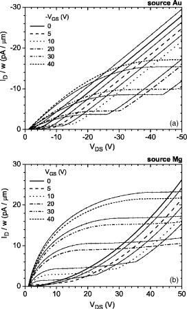
The measured ambipolar characteristics of the device fabricated are shown in Fig. 2. Depicted are the output characteristics for Au wired as source Fig. 2 a and Mg wired as source Fig. 2 b . In both cases, the drain-source and the gate-source voltages have the same polarity, i.e., for Au as source both voltages are negative, whereas for Mg as source both are positive. Consequently, the Mg contact is always negatively biased relative to the Au contact. For Au as sourceFig. 2 a and a negative gate bias VGS, typical p-channel characteristics are observed for negative drain-source volt-
ages with VDS VGS,eff . With increasing VDS , an abrupt steep increase in the drain current ID is measured, which is a
typical characteristic of ambipolar operation in OFETs see
FIG. 2. Output characteristics of the heterostructure transistor, using as source contact either a Au or b Mg. With Au Mg as source, both the gate-source and the drain-source voltages have been chosen negative positive , leading to a p channel n channel for small drain-source voltage.
also Refs. 14Ð16 . The direction of the almost parallel shift of this steeply increasing current with increasing negative gate voltage clearly indicates an electron current, which consequently must be injected at the Mg drain. From the onset of this increase for different gate-source voltages, one obtains the threshold voltage Vth +12 V. As a further characteristic, the steep increase of the electron current for higher drain voltages is almost linear. For Mg as source and a positive gate bias Fig. 2 b , in addition to the n-channel formation at lower drain-source voltages, there is again an additional current for larger drain-source voltage due to hole injection at the Au drain. However, it only occurs for VGS
10 V, i.e., for VGS,eff 0 V. In this case, the drain voltage dependence is almost quadratic. This additional hole current
predominates only for drain-source voltages that are much larger than the onset voltage for the saturated electron current. This is in contrast to the case with Au as source. There, the additional electron current begins to predominate roughly at the onset of saturation of the hole current. Hence, the two onsets cannot be described by the same Vth. Furthermore, for the Mg source, the n-channel transistor current is much larger in this case than the p-channel current for the Au source Fig. 2 a . In contrast to the usual characteristics, this n-channel current increases in saturation almost linearly with the gate-source voltage, rather than exhibiting the normal quadratic dependence. A recent simulation study revealed that a Schottky-type source can cause such a dependence.27
Downloaded 27 Nov 2006 to 146.103.254.11. Redistribution subject to AIP license or copyright, see http://jap.aip.org/jap/copyright.jsp
084505-4 |
Paasch et al. |
J. Appl. Phys. 98, 084505 2005 |
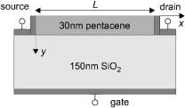
FIG. 3. Monolayer model structure.
Finally, deviations from the normal current characteristics at low drain-source voltages have to be mentioned: For Au as source Fig. 2 a , one has a soft onset of the current with a positive curvature changing only at a Þnite drainsource voltage into the normal negative curvature. For Mg as source Fig. 2 b and low drain-source voltages, the current increases sublinearly instead of the typical linear increase in the active transistor regime. Such a soft onset of the current has often been ascribed to series resistances.28 However, it has been shown, e.g. in Refs. 29 and 30, that contact resistances only cause a sublinear gate voltage dependence. Our simulations27 yielded the same conclusion. Additional series resistances act in the same direction. The problem of the soft current onset will be the subject of a subsequent article as it is not directly connected with ambipolar transport in the device.
For further details on the experimental results, the reader is referred to Ref. 16
III. TWO-DIMENSIONAL SIMULATION
A. Model systems
The double-layer device structure Fig. 1 was used to exploit the good electronand hole-conduction properties of different materials.15,16 Moreover, the larger afÞnity of the electron-transport layer favors electron injection at the Mg contact. Whether the heterojunction between the two active layers is advantageous remains to be clariÞed. In addition, the Mg electrode is not in direct contact with the channel, resulting in an Ohmic series resistance. To understand the processes in a double-injection transistor and the main parameters determining its performance, we analyze a simpliÞed monolayer model system with both source and drain as bottom contacts Fig. 3 . The two contact materials are metals with different work functions. Dimensions are chosen to be close to the double-layer system prepared. The two contacts are 30 nm thick; the thickness of the organic layer is d=30 nm, and the channel length is L=140 m. The simulated length is 160 m including the source and drain contact regions. In the simulations the channel width is generally w=1 m. The SiO2 gate insulator thickness is dox =150 nm with a relative dielectric constant of ox =3.9. For the active organic layer a model substance is introduced that has the same parameters as pentacene, however, both hole and electron mobilities are varied arbitrarily. In the following, this model substance will be denoted as Òpentacene.Ó In addition,
as reference system a diode has been considered that essentially is the same as the model transistor of Fig. 3, but without the gate and the gate dielectric.
B. Simulation method and standard material parameters
Simulations have been carried out using the driftdiffusion model. In this investigation, the two-dimensional device simulation program ISE-TCAD Ref. 31 is used. Its applicability to organic materials has been shown in detail in
Refs. 32Ð34, and several investigations of organic FETs have already been performed.27,35Ð38 The program simultaneously
solves the Poisson equation for the electrical potential and the continuity equations for the hole p and electron n densities. In the nondegenerate limit, the latter are connected
with the hole and electron quasi-Fermi potentials F |
and |
|
p |
Fn by p=ni exp e Fp − /kBT and n=ni exp e − Fn / |
|
kBT . The intrinsic density ni = NVNC exp −Eg /2kBT is con- |
|
nected with the gap energy Eg and the effective densities of states NV and NC. For a molecular material, the molecular or monomer density has to be used rather than the effective density of states.33
Material parameters of the pentacene layer have been chosen as follows: relative dielectric constant r =3.5, electron afÞnity =3.22 eV, band gap Eg =1.85 eV,24 and effective density of states NC =NV =1021 cm−3 monomer density . Constant mobilities for electrons and holes are assumed, but the absolute values are varied. Unless otherwise noted, n =1.2 10−3 cm2 /V s and p =1.2 10−4 cm2 /V s are used as standard values. The material is assumed to be intrinsic. However, calculations with a basic doping concentration of N−A =1016 and 1017 cm−3 have also been carried out for comparison. In addition, direct recombination was taken into account. For an organic material with low mobility, the bimo-
lecular recombination rate r described by the Langevin form39,40 is
Rdirect = r np − ni2 , |
1 |
||
with |
|
|
|
r = |
e |
n + p . |
2 |
|
|||
|
0 r |
|
|
The relevance of the recombination process was proved by simulations with and without its inclusion. The gate and source/drain materials are described as metals. The gate contact material is characterized solely by its work function. Here we have chosen 4.08 eV which corresponds to n+ −Si with a doping concentration of ND =8 1018 cm−3 as gate contact material. The exact value is not really of interest because only the ßatband voltage is directly inßuenced. In contrast, the work functions of the metallic source and drain contacts are crucial quantities and should be chosen individually to enable efÞcient injection of holes from one and electrons from the other contact. Thus, for one contactAu we have chosen 5.0 eV which is close to the valence band HOMO of pentacene. The work function for the other contact Mg has been varied between 3.68 and 3.57 eV. As standard value 3.635 eV is used. The difference between
Downloaded 27 Nov 2006 to 146.103.254.11. Redistribution subject to AIP license or copyright, see http://jap.aip.org/jap/copyright.jsp
084505-5 |
Paasch et al. |
J. Appl. Phys. 98, 084505 2005 |
these metal work functions and the energy of the transport states, i.e., for electrons and +Eg for holes where is the electron afÞnity acts as barrier at the contacts. Possible dipole layers or Fermi-level pinning can be modeled by choosing a corrected work function. For any given set of parameters, one simulation with the Au contact as source and one with Mg as source have been carried out. All results correspond to a temperature of 300 K.
For the standard barriers, the hole density at the Au contact is 6.6 1019 cm−3, whereas the electron density at the Mg contact is rather low, i.e., 1.0 1014 cm−3. Therefore, the Au contact will be an accumulation contact for holes. Its properties remain unchanged for small variation of its work function. On the other hand, at the Mg contact the channel is depleted and the electron current depends sensitively on the exact value of the Mg work function. In addition, the occurrence of both the electron current injected at Mg and the hole current injected at Au depends on the ratio of the electron and hole mobilities. The standard parameters used have been chosen such that the device clearly exhibits ambipolar properties.
IV. RESULTS
A. Ambipolar current characteristics
Current-voltage characteristics simulated with the standard parameters deÞned above are depicted in Figs. 4 and 5 for the Au and the Mg source, respectively. The output characteristics are shown in the upper panels a and the transfer characteristics in the lower panels b . The output characteristics qualitatively exhibit the same features of ambipolar behavior as the experimental dependencies do for the asymmetric heterostructure Fig. 2 , but there are also some differences.
In the output characteristic with Au as source Fig. 4 a , similar to Fig. 2 a , for negative VGS and lower negative drain-source voltage, one sees the typical p-channel characteristic up to where saturation sets in. For higher VDS , the steep almost linear increase of the current begins abruptly, with a gate-source voltage dependence that indicates an electron current, and an almost equidistant parallel shift with VGS. The onset of this increase is clearly at a lower drain
voltage than in Fig. 2 a , with a lower Vth +3 V. A shift of this onset voltage to larger negative drain-source voltage
can be caused by a negative interface charge see Sec. IV C 5 . The transfer characteristic Fig. 4 b for the p channel shows the normal linear dependence of the active region for low negative drain-source voltage and negative gatesource voltage. If the gate-source voltage is changed in the positive direction, the onset of the electron current occurs rather than the expected quadratic dependence of the saturation region. This electron current becomes larger than the hole current for increasing positive gate-source voltage owing to the higher electron mobility. On the other hand, the gate-source voltage dependence of this current becomes sublinear, as expected from a non-ohmic electron injecting contact here the Mg drain . Although the current reaches a minimum, there is no real off state.
FIG. 4. Simulated a output and b transfer characteristics for source at the Au contact. Standard parameters according to Sec. III B are used: Au work function 5.0 eV barrier for holes 0.07 eV , Mg work function 3.635 eVbarrier for electrons 0.415 eV , p =1.2 10−4 , n =1.2 10−3, direct Langevin recombination, and undoped organic layer. The drain current is given per unit channel width.
The output characteristic for Mg as source and a positive gate-source voltage Fig. 5 a shows, in addition to the n-channel formation at lower drain-source voltages, again an additional current for larger drain-source voltages arising from hole injection at the Au drain. Similar to Fig. 2 b , this onset is shifted to larger drain-source voltages and is visible only for low gate-source voltages. In good agreement with the experiments, the drain-voltage dependence of this hole channel current is almost quadratic. Also, the n-channel current increases in saturation almost linearly with the gatesource voltage, in contrast to the normal quadratic dependence. This is also visible in the transfer characteristic Fig. 5 b , which as for Au as source Fig. 4 b becomes sublinear for larger positive gate-source voltage, and again the hole channel current exhibits a linear gate-source voltage dependence.
To summarize, the simulated model system indeed qualitatively shows the characteristics typical for the ambipolar operation, which have been measured at the asymmetric heterostructure device. However, their origin can only be understood in detail by an inspection of the internal Þeld and concentration proÞles, given in Sec. IV B.
The two deviations of the measured characteristics from the theoretical description at low drain-source voltages, i.e.,
Downloaded 27 Nov 2006 to 146.103.254.11. Redistribution subject to AIP license or copyright, see http://jap.aip.org/jap/copyright.jsp
084505-6 |
Paasch et al. |
J. Appl. Phys. 98, 084505 2005 |
FIG. 5. Simulated a output and b transfer characteristics for source at the Mg contact. Standard parameters as in Fig. 4.
the soft onset of the current with a positive curvature for Au as source and the rather weak gate-source voltage dependence of the current for Mg as source, do not occur in the simulations owing to the simpliÞed description of the contacts.
B. Internal carrier and field distributions: Analysis of the ambipolar operation
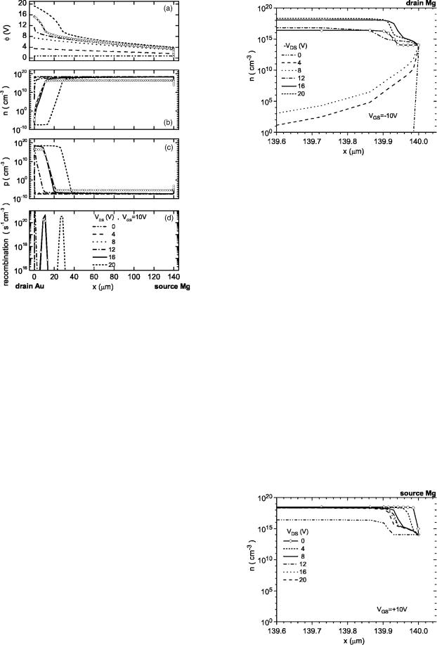
The internal device physics is described by three variables, the electrical potential, the electron, and the hole concentrations. They are shown in Figs. 6 a Ð6 c for Au as source contact along the channel at the interface to the gate oxide. The gate-source voltage VGS is −10 V and the negative drain-source voltage VDS is varied. The corresponding current-voltage characteristics are shown in Fig. 4. For low −VDS 8 V, the potential drops linearly active transistor region , the electron concentration is negligible, and only the p channel is formed with a carrier concentration 31018 cm−3, which is less than the concentration at the Au contact. At −VDS =12 V, the potential Þrst begins to decrease towards the Mg contact, as in the transition into saturation, but then the curvature changes, indicating the occurrence of the electron channel with an extension of 6 m. In this region the hole channel disappears. Already for −VDS =16 V, the electron channel spans about 90 m and the hole channel becomes correspondingly shorter. At −VDS =20 V
FIG. 6. ProÞles of a the potential, b the electron concentration, c the hole concentration, and d the recombination along the channel from Au source to Mg drain for the VGS =−10 V current-voltage characteristics of Fig. 4. Lines indicate proÞles 1 nm above the interface to the oxide for a variation of −VDS =0 4 20 V see inset in d . Lines with symbols indicate a proÞle 1 nm below the interface to vacuum for −VDS =16 V.
the onset of the electron channel is further shifted towards the source contact. The occurrence of the electron channel at −VDS =12 V is reßected in the corresponding output characteristic by the onset of the electron current Fig. 4 a . As expected, recombination occurs just at the transition between the two channels, i.e., for n p, as depicted in Fig. 6 d . Thus with increasing drain-source voltage, the recombination zone is shifted through the channel towards the Au source, and thereby recombination increases slightly. The length of the recombination zone is only few micrometer. For −VDS =16 V, the concentrations and the recombination rate at a position near the outer surface of the 30-nm-thick layer are shown by the symbols in this Þgure. In the corresponding regions of the two accumulation channels, the concentrations decrease across the layer by roughly two orders of magnitude from 2.3 1018 to 2.3 1016 cm−3; therefore the electrical current is conÞned in the accumulation layer, which is less than 10 nm thick. However, the maximum of the recombination at x 50 m occurs at the interface to the oxide at the rather low value n= p 5 1014 cm−3 Figs. 6 b and 6 c , which is also much less than the above-mentioned electron and hole concentration in the channel regions at the outer surface. Therefore, there are sufÞcient carriers at the outer surface to provide almost the same value n= p as at the interface to the oxide, hence the recombination rate is almost constant across the layer. Simulations for thicker layers, e.g.,
Downloaded 27 Nov 2006 to 146.103.254.11. Redistribution subject to AIP license or copyright, see http://jap.aip.org/jap/copyright.jsp
084505-7 |
Paasch et al. |
FIG. 7. ProÞles of a the potential, b the electron concentration, c the hole concentration, and d the recombination along the channel from Au drain to Mg source for the VGS = +10 V current-voltage characteristics of Fig. 5. Lines indicate proÞles 1 nm above the interface to the oxide for a variation of VDS =0 4 20 V see inset in d . Lines with symbols indicate a proÞle 1 nm below the interface to vacuum for VDS =16 V.
100 nm, show that the charge-carrier concentration across the layer decreases further, and therefore the recombination also begins to decrease towards the vacuum side of the layer. Similarly, also the extension of the recombination zone perpendicular to the layer is reduced for higher doping levels, owing to the reduced depletion length.
For Mg as source n channel at low drain voltages the corresponding dependencies are depicted in Fig. 7 with the interchange of source and drain and the changed sign of the potential. A signiÞcant difference to the previously discussed case of the Au source exists. Because of the higher electron mobility, the n channel is longer than the region of the injected holes near the drain even at VDS =20 V. Therefore, in the current characteristic for VGS =10 V, the hole current begins to predominate only above VDS 35 V. For the same reason, the location of the recombination moves only to a lesser degree from drain to source. Moreover, recombination is largest near the hole-injecting Au electrode, at a drainsource voltage at which the hole current is not yet visible in the current characteristics, and then decreases with the further increase of VDS.
However, these differences between the potential and density proÞles and their correlation with the current-voltage characteristics cannot explain the striking differences between the electron and hole currents described in the preceding section. Actually, there is one more difference visible in
J. Appl. Phys. 98, 084505 2005
FIG. 8. Detail of the electron concentration from Fig. 6 near the Mg drain.
Figs. 6 a and 7 a : Directly at the Mg contact as source or as drain there is an abrupt potential drop that increases withVDS . No such a potential drop occurs at the Au contact. The hole concentration at the Au contact is larger than in the accumulation channel, as discussed before. Thus the Au contact yields an excess of holes. For holes the Mg contact is a forward-biased Schottky contact. Therefore, if Au is the source, one obtains the normal p-channel transistor characteristic for small VDS Fig. 4 . With Au as drain and for sufÞciently large VDS , i.e., where the hole channel predominates, the device operates similarly as a forward-biased diode under space-charge-limited condition, leading to the quadratic VDS dependence. This is similar to normal space- charge-limited current SCLC . Nevertheless, the presence of the gate modiÞes the operation signiÞcantly, as will be discussed in Sec. V. The situation is rather different if the Mg contact provides electron injection. In Figs. 8 and 9, the electron density of Figs. 6 b and 7 b is shown directly near this contact in the rather small 400 nm region of the 140- m-long channel. For Mg as source Fig. 9 the n channel exists because of the applied gate voltage, and, owing to the Mg work function this contact is a reverse-biased Schottky contact for electrons, with a depletion zone growing with increasing VDS. This depletion at source limits the n-channel transistor current, as discussed in connection with
FIG. 9. Detail of the electron concentration from Fig. 7 near the Mg source.
Downloaded 27 Nov 2006 to 146.103.254.11. Redistribution subject to AIP license or copyright, see http://jap.aip.org/jap/copyright.jsp
084505-8 |
Paasch et al. |
J. Appl. Phys. 98, 084505 2005 |
Fig. 5, and is also responsible for the non quadratic dependence of the current on the gate voltage. This effect of a Schottky-type source has been described already in Ref. 27. For Mg as drain Fig. 8 the n channel is formed only at larger VDS , but then one has again a reversed-biased Schottky contact with this channel, the depletion zone increases with increasing VDS cf. −16 and −20 V . The narrow depletion zone with an extension just below 100 nm in series with the long accumulation channel effectively act as ohmic resistance with a linear dependence on the drainsource voltage.
All these properties occur for the set of parameters chosen, especially for the ratio of the mobilities chosen and the work functions of both contacts. Variation of these and other parameters will be discussed next.
C. Variation of doping, contact properties, mobilities, and recombination characteristics
1. Influence of doping
As shown in the preceding section, the simulations for the single-layer model system without doping of the active layer already yield the main ambipolar characteristics measured in the heterostructure device. As the active layers have been vacuum deposited, low or even negligible doping can be assumed. This might not be the case if a conjugated polymer is used, which often appears to be unintentionally p doped. Therefore, simulations have been carried out that assume additional, completely ionized acceptors with a density of N−A =1016 and 1017 cm−3. The resulting modiÞcation of the current-voltage characteristics were marginal for the lower doping. For the higher doping level the output characteristics are compared in Figs. 10 a and 10 b to those without doping in Figs. 4 a and 5 a , respectively. Clearly, there is no qualitative modiÞcation, however, in both cases the hole current is slightly enhanced and the electron current decreased. Thereby the onsets of the currents injected at the drain are shifted upward by several volts. This shift is nearly the same
as the threshold voltage shift, V |
th |
= V |
FB |
+eN−d/C |
|
|||||||
|
|
|
|
|
|
A |
|
ox |
||||
−2 b d/ldep 2, with the organic layer thickness d, the deple- |
||||||||||||
tion length l |
dep |
, the gate oxide capacitance C |
= |
0 |
|
ox |
/d |
ox |
, |
|||
|
|
|
|
ox |
|
|
|
|
||||
and the bulk potential b. For the given parameters and the doping level in Fig. 10 one obtains Vth =1.5 V.
2. Variation of the Mg contact
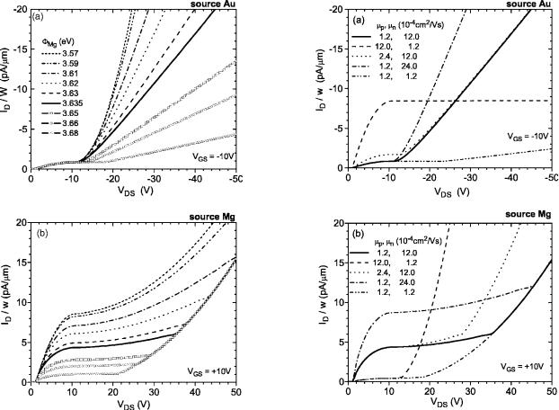
The inßuence of a variation of the Mg work function in the narrow region Mg =3.57¯3.68 eV the standard value was Mg =3.635 eV is demonstrated in Fig. 11 with the current-voltage characteristics VGS =10 V for Mg a as drain and b as source. For Mg as drain, for low VDS , the p-transistor channel current is unaffected. The onset of the electron current injected at drain is shifted to lower VDS with decreasing work function, i.e., decreasing barrier for electrons. Simultaneously, for larger VDS the slope of the injected electron current increases. Comparing the slopes of the almost linear dependence, e.g., for Mg =3.63 and 3.68 eV, one obtains a ratio of about 6.9 from Fig. 11 a . This is almost the same as the ratio of the electron concentrations at the contact for the two values of the work functions:
FIG. 10. Simulated output characteristics for the source at a the Au contact and b at the Mg contact without doping line with symbols as in Figs. 4 a and 5 a and with completely ionized acceptors of density 1017 cm−3 line without symbols .
exp Mg /kBT =exp 0.05/0.0258 =6.94. This indicates that this slope and hence this current essentially are determined only by the tiny region of the reduced electron concentration near the Mg contact cf. Fig. 8 . For Mg as sourceFig. 11 b the n-channel transistor current for lower drainsource voltages increases strongly with decreasing electron barrier, i.e., decreasing work function, which could be misinterpreted as a difference in the mobilities.
3. Variation of the mobilities
The large inßuence of the mobilities has been discussed in Secs. IV A and IV B. The inßuence of a variation of the two mobilities the standard values were p =1.2 10−4 andn =1.2 10−3 cm2 /V s is demonstrated in Fig. 12 with the current-voltage characteristics VGS =10 V for a Au as source and b Mg as source. Interchanging the two values for the mobilities leads to the disappearance of the electron current injected at the Mg drain or the onset is shifted above the drain voltage region considered and the p-channel current at the Au source exhibits good saturation at higher current level, whereas if the source is Mg the n-channel current is reduced and the onset of the hole current injected at the Au drain is shifted to lower VDS . The other variations in Fig. 12 conÞrm the following tendencies: The onset of the draininjected current is shifted to lower VDS for higher mobility
Downloaded 27 Nov 2006 to 146.103.254.11. Redistribution subject to AIP license or copyright, see http://jap.aip.org/jap/copyright.jsp
084505-9 |
Paasch et al. |
J. Appl. Phys. 98, 084505 2005 |
FIG. 11. Simulated output characteristics for the source at a the Au contact and at b the Mg contact for VGS = ±10 V with a variation of the Mg work function as indicated in the legend, otherwise standard parameters as in Fig. 4.
FIG. 12. Simulated output characteristics for source at a the Au contact and at b the Mg contact for VGS = ±10 V with a variation of the electron and hole mobilities as indicated in the legend, otherwise standard parameters as in Fig. 4.
of the corresponding carriers; the slope of the linear increase of the electron current injected at the Mg drain is proportional to the electron mobility in the region of reduced electron concentration near the drain that determines this current, see preceding section , and the curvature of the SCLClike hole current injected at the Au drain increases with the mobility.
In general, a large variety of current characteristicsshown in Fig. 12 for one gate-source voltage only is obtained by varying the mobilities for a given electron barrier. Even slight modiÞcations of the mobilities e.g., by a chemical modiÞcation of the organic layer help to improve the ambipolar device operation.
4. Influence of recombination
So far in the simulations, direct Langevin recombination has been taken into account according to Eqs. 1 and2 , whereas earlier models neglected recombination. Output characteristics simulated for zero recombination are shown in Fig. 13 for source at a the Au contact and b the Mg contact. The corresponding dependencies with recombination are those in Figs. 4 a and 5 a . For the Au source, the normal hole current for low VDS without recombination is almost unchanged, but the onset of the electron current injected at the Mg drain is shifted to lower VDS . For the Mg
source contact, neglecting recombination leads to qualitatively different output characteristics with an additional hump and no clear shift of the hole current injected at the Au drain with VGS , in contrast to the dependence of the measurements Fig. 2 b . Consequently, describing experimental data with models without recombinationÑif at all possibleÑwill inevitably lead to inappropriate values for the other model parameters.
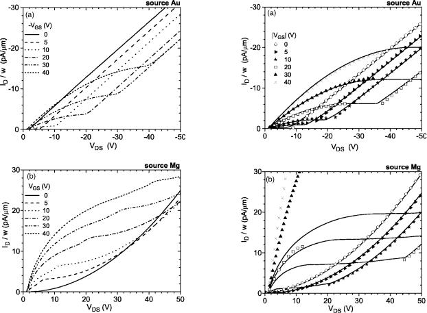
5. Influence of an interface charge
Although the simulations for the single-layer model system already yield the important characteristics of ambipolar operation, see Fig. 2, there is one striking difference between the experimental curves and the simulations. For Au as source, the onset of the electron current injected at the Mg drain occurs in the experiment Fig. 2 a at much larger drain-source voltages than in the simulations Fig. 4 a . Such a shift can be caused by an areal charge at the interface between the gate insulator and the active organic layer, which is known to shift the threshold voltage in a FET. The inßuence of an interface charge on the output characteristics is depicted in Fig. 14, shown by solid lines the symbols will be discussed in Sec. V . In addition to the standard parameters used in Fig. 4, a negative interface charge Qif =−81011 e cm−2 is taken into account. For Au as source, the
Downloaded 27 Nov 2006 to 146.103.254.11. Redistribution subject to AIP license or copyright, see http://jap.aip.org/jap/copyright.jsp
084505-10 Paasch et al. |
J. Appl. Phys. 98, 084505 2005 |
FIG. 13. Simulated output characteristics for source at a the Au contact and at b the Mg contact. Standard parameters as in Fig. 4, but without recombination.
comparison with Fig. 4 a shows an enhanced hole current for smaller VDS , a shift of the onset of the drain-injected electron current to larger VDS as in the experiment, and correspondingly for larger VDS a lower electron current. The reason is simply that this negative interface charge attracts additional holes in the channel and repels electrons. For the same reason, in the case of Mg as source, the electron current at lower VDS is reduced compared to the values in Fig. 5 a , the onset of the hole current injected at the Au drain is shifted to lower VDS, and for a larger VDS the hole current is enhanced.
The large shift of the onset of the drain-injected electron current in the experiments Fig. 2 a with the heterostructure transistor clearly indicate that in this particular device a negative interface charge was present.
V. DIRECT PARAMETER EXTRACTION:
POSSIBILITIES AND LIMITATIONS
For the direct extraction of material parameters from measured current-voltage characteristics, one needs simple but reliable analytical models. Extracted parameters can be used also as initial input parameters in numerical simulations. For the analysis of measurements on OFETs in most
FIG. 14. Simulated output characteristics for source at a the Au contact and at b the Mg contact as Figs. 4 a and 5 a . Standard parameters as in Fig. 4, in addition a negative interface charge Qif =−8 1011 ecm−2 has been included. Solid lines: Simulation; and symbols: piecewise analytical models
with Eq. 4 for lower VDS in a and b , and for larger VDS Eq. 5 in a and Eq. 6 in b . Gate-source voltages indicated are negative in a and
positive in b .
cases the simple Shockley model is applied.41 Here the drain current above threshold of the transistor depends on the drain-source and gate-source voltages as
|
|
w |
C |
|
V |
|
− V |
|
V |
|
− |
1 |
V2 |
, |
V |
|
V |
|
− V |
|
|
|
|
GS |
th |
DS |
|
DS |
GS |
th |
|||||||||||
|
|
L ox |
|
|
|
|
2 DS |
|
|
|
|
|||||||||
ID = |
w |
1 |
|
|
|
|
|
|
|
|
|
|
|
|
|
|
|
3 |
||
|
VGS − Vth 2, |
|
|
|
|
VDS VGS − Vth. |
||||||||||||||
|
|
Cox |
|
|
|
|
|
|||||||||||||
|
L |
2 |
|
|
|
|
||||||||||||||
Clearly, for the ambipolar FET, one at least has to replace the expression for the saturation region in order to describe the current injected at the drain.
One advantage of numerical simulations is that they can be used to check the reliability of models as the material parameters are known from the input data. This will be done here using the simulated output characteristics for the system with an additional interface charge Fig. 14 . For the thin undoped layer considered here, one has, according to Ref. 38, Vth VFB. Using the parameters from Sec. III B, we obtain VFB =0.065 V, which can be neglected. Owing to the difference in the work functions of source and drain, one has to replace VDS by VDS −Vbi with the built in potential Vbi = Mg − Au /e. The interface charge is connected with an
Downloaded 27 Nov 2006 to 146.103.254.11. Redistribution subject to AIP license or copyright, see http://jap.aip.org/jap/copyright.jsp