

nanotechnology / AM1
.PDFOrganic Thin Film Transistors for Large Area Electronics
By Christos D. Dimitrakopoulos*
and Patrick R. L. Malenfant
Organic thin-film transistors (OTFTs) have lived to see great improvements in recent years. This review presents new insight into conduction mechanisms and performance characteristics, as well as opportunities for modeling properties of OTFTs. The shifted focus in research from novel chemical structures to fabrication technologies that
optimize morphology and structural order is underscored by chapters on vacuum-deposited and solution-pro- cessed organic semiconducting films. Finally, progress in the growing field of the n-type OTFTs is discussed in ample detail. The Figure, showing a pentacene film edge on SiO2, illustrates the morphology issue.
1. Introduction
Organic semiconductors have been studied since the late 1940s.[1] However, until recently they had failed to have a significant practical impact in optoelectronic applications, despite of the fact that a very large number of experimental and theoretical studies have been published. Initial industrial applications of organic semiconductors exploited their photoconductive properties in xerography. The initial demonstration of organic electroluminescent diodes[2,3] and OTFTs[4±6]
based on either small organic molecules[2,5] or conjugated polymers,[3,4,6] and the impressive improvements in perfor-
mance, and efficiency of organic devices during the last decade[7±10] attracted the interest of industry and opened the
way to practical applications for organic semiconductors. In this review we will focus on the progress in the field of OTFTs in recent years. We will restrict our review to transistors in which the organic active layer is an approximately two-dimen- sional structure, such as a thin film. It has been shown that
only a few organic monolayers are sufficient for proper transistor operation.[11,12] We will make an effort to describe the
broad spectrum of materials, fabrication processes, designs, and applications of OTFTs, with an emphasis on papers published during the last few years. Older papers that, in the authors' opinion, played a pivotal role in shaping the OTFT
±
[*]Dr. C. D. Dimitrakopoulos, Dr. P. R. L. Malenfant[+] IBM Corporation, T. J. Watson Research Center P.O. Box 218, Yorktown Heights, NY 10598 (USA) E-mail: dimitrak@us.ibm.com
[+]Present address: GE CRD, Emerging Technologies, K1-4A49, 1 Research Circle, Niskayuna, NY 12309, USA.
field are also reviewed, but the reader is encouraged to look
up a number of previously published review papers that cover that earlier period in more detail.[13±19] Reported results from
single crystal organic field effect transistors will be used to define the upper limit of performance of OTFTs and to gain a better understanding of the underlying device physics. Results from devices in which the active channel consists of a single organic molecule or a more extended structure such as a car-
bon nanotube, will not be discussed, despite the strong interest that recently has developed for such transistors.[20±24]
As in traditional inorganic semiconductors, organic materials can function either as p-type or n-type. In p-type semiconductors the majority carriers are holes, while in n-type the majority carriers are electrons. The most widely studied organic semiconductors have been p-type, however, due to the recent appearance of several new reports on OTFTs based on n-type organic semiconductors, we have devoted a separate section of this review to n-type organics. Pentacene, one of the most widely studied organic semiconductors for OTFTs, is used to demonstrate many of the physical phenomena discussed in this review, due to its superior field effect mobility and environmental stability, although a broad spectrum of organic semiconducting materials is also covered.
OTFTs based on conjugated polymers, oligomers, or fused aromatics have been envisioned as a viable alternative to more traditional, mainstream thin film transistors (TFTs) based on inorganic materials. Because of the relatively low mobility of organic semiconductors, OTFTs cannot rival the performance of field-effect transistors based on single-crystal- line inorganic semiconductors, such as Si, Ge, and GaAs, which have charge carrier mobilities (l) of three or more orders of magnitude higher.[25] Consequently, OTFTs are not suitable for use in applications requiring very high switching
REVIEW
Adv. Mater. 2002, 14, No. 2, January 16 |
Ó WILEY-VCH Verlag GmbH, D-69469 Weinheim, 2002 0935-9648/02/0201-0099 |
$ 17.50+.50/0 |
99 |
REVIEW
C. D. Dimitrakopoulos, P. R. L. Malenfant/Organic Thin Film Transistors
speeds. However, the unique processing characteristics and demonstrated performance of OTFTs suggest that they can be competitive candidates for existing or novel thin film transistor applications requiring large area coverage, structural flexibility, low temperature processing, and especially low cost. Such applications include switching devices for active matrix flat panel displays (AMFPDs) based on liquid crystal pixels (AMLCDs), organic light emitting diodes (AMOLEDDs), or ªelectronic paperº displays[26] based on pixels comprising either electrophoretic ink-containing microcapsules[27] or ªtwisting ballsº.[28] Additionally, sensors,[29] low-end smart cards, and radio-frequency identification tags (RFIDs) consisting of organic integrated circuits have been proposed and
prototype all-polymer integrated circuits have been demonstrated.[30]
Different applications will require different performance standards. At present, the entrenched technology in large area electronics applications, especially backplanes of AMLCDs, is based on TFTs comprising hydrogenated amorphous silicon (a-Si:H) active layers. However, OTFTs can enable applications that are not achievable using the entrenched technology, taking advantage of the fact that OTFTs, can be processed at or close to room temperature (RT) and thus are compatible with transparent plastic substrates. Because of the high processing temperature used during a-Si:H deposition (ca. 360 C), it is not possible to make an AMLCD based on such TFTs on a transparent plastic substrate. For OTFTs to compete directly with a-Si:H TFTs, the former should exhibit device performance similar to that of the latter, i.e., field
effect mobility l = 1 cm2 V±1 s±1, and current modulation (or
on/off ratio, Ion/off) of 106 or higher at a maximum operating voltage of about 15 V or less. Additionally, they should be
stable after prolonged exposure to ambient conditions, and should not exhibit large threshold voltage shifts.
2. Progress in Performance of p-Type Organic Thin-Film Field-Effect Transistors from 1984 to the Present Time
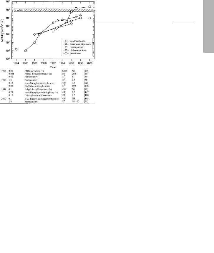
In a previous paper[7a] we presented a semi-logarithmic plot of each year's highest reported field-effect mobility value from TFTs based on various organic semiconductors since 1986. An updated and more complete version of that plot, based on Table 1 that includes results from p-type organic semiconductors only, is shown in Figure 1.
Table 1 lists the highest field-effect mobility (l) values measured from p-type OTFTs as reported in the literature, annually from 1984 to the present time, for each one of the most promising p-type organic semiconductors. For a specific p-type organic semiconductor that already has an entry in Table 1 and Figure 1 for a previous year, a new mobility value is entered only if it is higher than the value of the preceding entry. We can observe an impressive increase in mobility, which came about either by improving the processes used for the fabrication of the transistors or by synthesizing new organic materials. A typical path to performance increase could be described as a three-stage process: a) A new organic semicon-
Dr. Christos Dimitrakopoulos is a Research Staff Member at IBM, T. J. Watson Research Center, Yorktown Heights, NY, USA, where he works on organic semiconductor devices and circuits. He has been with IBM since 1995. From 1993 to 1995 he was a post-doctoral fellow at Philips Research Laboratories in Eindhoven, The Netherlands, where he also worked on organic semiconductors. He holds Ph.D., M.Phil., and M.Sc. degrees in Materials Science from Columbia University. He also holds a B.Sc. Degree in Metallurgical Engineering from the National Technical University of Athens, Greece. He is the author or co-author of four patents, seven pending patents and at least 20 papers. He has received an IBM Outstanding Innovation Award, for ªHigh Performance Organic Transistors on Plasticº.
Dr. Patrick Roland Lucien Malenfant was born in 1971 in Kapuskasing, Ontario and was raised in Timmins, Ontario, Canada until he attended college. He obtained his B.Sc. Honours co-op degree in Chemistry from the University of Ottawa in 1995. He received a M.S. from Cornell University in 1997 and a Ph.D. degree from the University of California at Berkeley in 2000 with Jean M. J. FrØchet. The main focus of his thesis was the synthesis of well-defined conjugated oligothiophenes and their combination with dendrimers. New synthetic methods were also devised that led to the first solid-phase synthesis of oligothiophenes. After graduation, he took a post-doctoral position at IBM's T. J. Watson Research Center in Yorktown Heights, NY where he worked in the area of organic electronics. He is currently working at GE Corporate Research and Development (CRD) in Niskayuna, NY as a member of the Emerging Technologies group.
100 |
Ó WILEY-VCH Verlag GmbH, D-69469 Weinheim, 2002 0935-9648/02/0201-0100 |
$ 17.50+.50/0 |
Adv. Mater. 2002, 14, No. 2, January 16 |
C. D. Dimitrakopoulos, P. R. L. Malenfant/Organic Thin Film Transistors
Table 1. The highest field-effect mobility (l) values measured from p-type OTFTs as reported in the literature, annually from 1984 to the present time, for each one of the most promising p-type organic semiconductors.
[a] Measured at RT. [b] (v) = vacuum deposition, (s) = from solution. [c] Values for Ion/Ioff correspond to different gate voltage ranges and thus are not readily comparable to each other. The reader is encouraged to read the details of the experiments in the cited references. [d] NR = not reported. [e] This result has not yet been reproduced.
obtain the most advantageous structural and morphological characteristics for improved performance until no more improvement seems possible. c) The source and drain contacts and the general transistor configuration are optimized. After this point, another incremental improvement in mobility is usually obtained from the synthesis and/or first OTFT application of a new organic semiconductor. Today, we have reached an important point in the performance versus time plot. The most widely used organic semiconductors, such as pentacene, thiophene oligomers, and regioregular poly(3-al- kyl-thiophene), seem to have reached ªmaturityº as far as their performance is concerned. Their individual performance versus time curves seem to have saturated (re: when a new, higher value is not reported in the years following the last entry for a material, it means that there was no improvement in mobility during those years). In the past, each time such a performance saturation occurred (Fig. 1), a new material was introduced whose performance broke the temporarily established upper limit in performance.
For instance, one can argue that today's maximum hole field effect mobility of 2.4 cm2 V±1 s±1 for OTFT (pentacene, measured at RT)[31] has approached a fundamental limit, at least as far as the known classes of semiconducting organic materials are concerned. This pentacene thin film was grown from the vapor phase in a stream of flowing gas (hydrogen or
forming gas), in an apparatus similar to the one described in the literature[32±35] and its grain size exceeded the channel
length (L) of the TFTs used to determine the field effect mobility. Consequently, this value is very close to RT field
effect mobility values of 3.2 and 2.7 cm2 V±1 s±1 reported by Schön et al.,[31,36] for holes in pentacene single crystals grown
from the vapor phase under hydrogen or forming gas flow,
while the substrate was held at relatively high temperature.[34,35] In the following section we will discuss the potential
existence of a fundamental limit for charge carrier mobility in conjunction with the various conduction mechanisms believed to be in operation in various organic semiconductors.
Fig. 1. Evolution of OTFT hole mobility for the most common p-type organic semiconductors. The various p-type materials are grouped together into families of similar molecules taking into account only the core part of each molecule. For reference, a representative range of electron mobilities for a-Si:H TFT is shown. The hole mobility in a-Si:H TFT is much lower than the electron mobility.
ductor is synthesized or a known one is used for the first time as the active layer in an OTFT. b) The film deposition parameters for the semiconducting organic layer are optimized to
3. Conduction Mechanisms in Organic
Semiconductors
The upper limit of microscopic mobilities in organic molecular crystals, determined at 300 K by time-of-flight (TOF) experiments, falls between 1 and 10 cm2 V±1 s±1.[1] The weak intermolecular interaction forces in organic semiconductors, typically van der Waals interactions with energies smaller than 10 kcal mol±1, may be responsible for this limit, since the vibrational energy of the molecules reaches a magnitude close to that of the intermolecular ªbondingº energies at or above RT. In contrast, in inorganic semiconductors such as Si, Ge, and GaAs, the atoms are held together with very strong covalent bonds, which in the case of Si have energies as high as 76 kcal mol±1. In these semiconductors, charge carriers move
as highly delocalized plane waves in wide bands and have a very high mobility at RT (l ~ 103 cm2 V±1 s±1). In this case, the
REVIEW
Adv. Mater. 2002, 14, No. 2, January 16 |
Ó WILEY-VCH Verlag GmbH, D-69469 Weinheim, 2002 0935-9648/02/0201-0101 |
$ 17.50+.50/0 |
101 |
REVIEW
C. D. Dimitrakopoulos, P. R. L. Malenfant/Organic Thin Film Transistors
mobility is limited by lattice vibrations (phonons) that scatter the carriers and thus it is reduced as the temperature increases.
Band transport is not applicable to disordered organic semiconductors, where carrier transport takes place by hopping between localized states and carriers are scattered at every step. Hopping is assisted by phonons and the mobility increases with temperature, although typically it remains very low overall (l << 1 cm2 V±1 s±1). The boundary between band
transport and hopping is defined by materials having RT mobilities of the order of 1 cm2 V±1 s±1.[1,18,37] Thin films of
highly ordered organic semiconductors, such as several mem-
bers of the acene series including pentacene, have RT mobilities in this intermediate range.[37±39] In some cases tempera-
ture independent mobility has been observed,[1] even in polycrystalline thin films of pentacene.[37] This observation was used to argue that a simple thermally activated hopping mechanism can be excluded as a transport mechanism in highquality polycrystalline thin films of pentacene despite of the fact that in some samples containing a large concentration of traps related to structural defects and chemical impurities the mobility increases with temperature.[37] Trapping at the grain boundaries in polycrystalline films of pentacene and the dependence of trap concentration on the film deposition conditions has been suggested as the main cause of the observed variability of the temperature dependence of mobility.[31]
Understanding the transport mechanism in single crystals of organic semiconductors will facilitate our understanding of transport in the technologically more relevant polycrystalline thin films of these materials. At low temperatures, coherent band-like transport of delocalized carriers becomes the prevalent transport mechanism in single crystals of pentacene, tetracene, and other acenes. Very high mobility values have been
measured using TOF experiments (up to 400 cm2 V±1 s±1 for holes in single crystals of naphthalene at 4.2 K)[40,41] and field
effect experiments (up to ~105 cm2 V±1 s±1 for holes in single crystals of tetracene and pentacene at 1.7 K).[31,42] In the latter
experiments, the mobility increases from its RT value of approximately 3 cm2 V±1 s±1 to about 105 cm2 V±1 s±1 at 1.7 K following a power law (l µ T±n, n = 2.7),[36,42,43] in agreement with earlier work in which n = 2.9 was reported.[41,44] At 1.7 K
an effective electronic bandwidth of ~0.5 eV (>>kBT, where kB is the Boltzmann constant) is estimated from the low effective mass for holes, measured to be of the order of 1 to 1.5me, where me is the free electron mass.[42] Furthermore, both the integer and fractional quantum Hall effects were observed in acene single crystals.[42] All this is clear evidence of band transport, at low temperatures, in such crystals. In 1974, Burland observed cyclotron resonance of holes in high quality sin-
gle crystals of anthracene at 2 K, the first time such an observation was made in a wide band gap molecular crystal.[45,46]
From the reported values of the effective mass of holes, m*, in these crystals, determined to be 11me, where me is the free
electron mass, and the hole scattering time, s, measured to be ~7 ” 10±11 and 4 ” 10±10 s, respectively in two different anthra-
cene crystals, one could calculate hole mobility values of
about 11 200 and 64 000 cm2 V±1 s±1, using the formula: l = (e m*±1)s, where e is the elementary charge. This was the first time that evidence of such enormously high charge carrier mobility values in organic semiconductors was presented.[45] The temperature dependence of the electron mobility in pentacene and tetracene single crystals was shown to follow the same power law that describes the hole mobility temperature dependence in the same materials, from 1.7 to 300 K. From all the work presented above, it is apparent that extremely high quality, ultra pure single crystals of organic semiconductors are required to obtain such high mobilities and observe the described phenomena. This behavior is rather impossible to observe in polycrystalline films when transport through two or more grains is studied, because traps attributed to grain boundaries and other structural defects dominate transport. Experiments that study electrical transport through only one individual crystallite (grain), which is part of a polycrystalline film, are considered here to be studies of electrical transport in organic semiconductor single crystals.
The temperature dependence of the electron mobility in naphthalene single crystals below 100 K also follows a power law along all three principal directions in the crystal, although
with a lower exponent (l µ T±n, n » 1.5 to 1.7), consistent with the band model.[40,44,47] However, between 100 K and 300 K
the electron mobility along the c crystallographic direction remains practically constant.[44,47,48] The l(T) = constant
region has been described phenomenologically as the superposition of two independent carrier mechanisms. According to one interpretation the first mechanism is described using the concept of an adiabatic, nearly small molecular polaron (MP),[47] which is an alternative way to rationalize the power law dependence alongside the delocalized band transport model. According to this model the carriers are treated as heavy polaron-type quasiparticles, which are formed as a result of the interaction of the carriers with intramolecular vibrations of the local lattice environment, and move coher-
ently via tunneling. In this model the mobility follows the power law lMP = aT±n.[47] The second mechanism involves a
small lattice polaron (LP), which moves by thermally activated hopping and thus exhibits a typical exponential dependence of mobility on temperature: lLP = bexp[±Ea/kT]. The superposition of these two mechanisms can reproduce the
experimentally measured temperature dependence of mobility from just a few degrees K to RT.[47]
Band-like transport of delocalized carriers is also shown to be the prevalent transport mechanism along the crystal directions with high p±p* orbital overlap, in single crystals of a-sex- ithiophene (6T) and a-quaterthiophene (4T).[43]
In the following sections we will discuss carrier transport in various polycrystalline thin films of organic semiconductors, assuming that transport in individual crystallites in the film takes place according to the mechanisms described in this section.
At this point we can propose two possible ways for eliminating the potential fundamental upper limit of about 10 cm2 V±1 s±1 for the RT mobility of OTFTs, imposed by the
102 |
Ó WILEY-VCH Verlag GmbH, D-69469 Weinheim, 2002 0935-9648/02/0201-0102 |
$ 17.50+.50/0 |
Adv. Mater. 2002, 14, No. 2, January 16 |

C. D. Dimitrakopoulos, P. R. L. Malenfant/Organic Thin Film Transistors
weak intermolecular forces existing among nearest-neighbor (nn) molecules. One is to strengthen such interactions. This can be done by creating a stronger bond between nn molecules. However, this has to take place without breaking the conjugation of the molecules, and without reducing the intermolecular overlap between nn molecules. Stronger intermolecular interactions would result in more rigid crystalline structures, and thus it would take temperatures higher than RT to generate substantial scattering of highly delocalized carriers by lattice vibrations. Using such a strategy, one, in effect, could produce at RT, mobility values comparable to the high mobility that exists at very low temperatures in crystals of the acene series, or at worse considerably higher than their RT mobilities. A second way involves a more drastic change in the conduction path and mechanism. It involves carrier transport via an array of single molecules, such as nanotubes or polymer chains that would bridge the gap between the source and drain electrodes of a TFT. Intermolecular transport is replaced by intramolecular transport. This would require a drastic reduction in the size of the TFT channel from micrometer-size to nanometer-size so that it is shorter than the length of a single molecule. Recently,
TFTs based on carbon nanotubes have been constructed and mobilities are of the order of 100 cm2 V±1 s±1.[24] This is an
excellent example of the potential effectiveness of this strategy. The successful execution of any one of these strategies would prove that the existing performance limits are partially imposed by the design and size of OTFTs, and not by the inherent properties of organic materials.
mode over the current in the depletion mode, also referred to as Ion/Ioff ratio), and the threshold voltage, VT. Polycrystalline pentacene OTFTs exhibit p-type behavior (the majority carriers are holes). Thus, when the gate electrode is biased positively with respect to the grounded source electrode, they operate in the depletion mode, and the channel region is depleted of carriers resulting in high channel resistance (off state). When the gate electrode is biased negatively, they operate in the accumulation mode and a large concentration of carriers is accumulated in the transistor channel, resulting in low channel resistance (on state). For n-type TFT operation, the electrode polarity is reversed and the majority carriers are electrons instead of holes.
A typical plot of drain current ID versus drain voltage VD at various gate voltages VG is shown in Figure 3, which corresponds to a top-contact OTFT (Fig. 2a) using a polycrystalline, vapor deposited pentacene film as the semiconductor, 5000 Š thermally grown SiO2 modified with a 1-diethoxy-1-silacyclo-
4. Modeling of the Electrical Characteristics of Organic Thin-Film Field-Effect Transistors
Figure 2 shows two common device configurations used in OTFTs. The I±V characteristics of OTFTs can be adequately
described by models developed for inorganic semiconductors[49] as shown earlier.[7a,16,18,50±52] Polycrystalline pentacene
OTFTs are used here to demonstrate typical I±V characteristics of OTFTs and the methods used to calculate the field effect mobility and other device parameters such as the current modulation (the ratio of the current in the accumulation
Fig. 2. OTFT device configurations: a) Top-contact device, with source and drain electrodes evaporated onto the organic semiconducting layer through a mask. b) Bottom-contact device, with the organic semiconductor deposited onto the gate insulator and the prefabricated source and drain electrodes.
Fig. 3. Plot of a drain current ID versus drain voltage VD at various gate voltages VG from a top-contact OTFT comprising a polycrystalline pentacene thin film channel, a 5000 Š thick SiO2 gate insulator layer modified with a 1-diethoxy-1-silacyclopent-3-ene SAM, a heavily doped n-type Si wafer as the gate, and Au source and drain electrodes. The linear regime mobility is
0.80 cm2 V±1 s±1 at VD = ±10 V, and the saturation regime mobility is 1.03 cm2 V±1 s±1 at VD = ±100 V. L = 15.4 lm and W = 1 mm.
pent-3-ene self-assembled monolayer (SAM)[53] as the gate insulator, a heavily doped n-type Si wafer as the gate, and gold source and drain electrodes.[54] At low VD, ID increases linearly with VD (linear regime) and is approximately determined from the following equation:
ID = Li |
|
VG ÿ VT ÿ 2 |
!VD |
(1) |
||
|
WC |
l |
|
VD |
|
|
where L is the channel length, W is the channel width, Ci is the capacitance per unit area of the insulating layer, VT is the threshold voltage, and l is the field effect mobility, which can be calculated in the linear regime from the transconductance,
|
@I |
|
|
|
WC |
|
|
gm = |
D |
|
ˆ |
i |
lVD |
(2) |
|
@V |
|
L |
|||||
|
G |
V |
const: |
|
|
|
|
|
|
|
D ˆ |
|
|
|
|
|
|
|
|
|
|
|
|
|
|
|
|
|
|
|
|
REVIEW
Adv. Mater. 2002, 14, No. 2, January 16 |
Ó WILEY-VCH Verlag GmbH, D-69469 Weinheim, 2002 0935-9648/02/0201-0103 |
$ 17.50+.50/0 |
103 |
REVIEW
C. D. Dimitrakopoulos, P. R. L. Malenfant/Organic Thin Film Transistors
by plotting ID versus VG at a constant low VD, with ±VD << ±(VG ± VT), and equating the value of the slope of this plot to gm. The calculated linear mobility value is 0.80 cm2 V±1 s±1 at VD = ±10 V, which is a high value compared to previously published values of linear regime mobility from polycrystalline OTFTs. The value of VD is chosen so that it lies in the linear part of the ID versus VD curve. For this device L = 15.4 lm and W = 1 mm.
For ±VD > ±(VG ± VT), ID tends to saturate (saturation regime) due to the pinch-off of the accumulation layer, and is
modeled by the equation |
|
||||
ID = |
WCi l |
…VG ÿ VT † |
2 |
(3) |
|
2L |
|
|
|||
In the saturation regime, l can be calculated from the slope p•••••••••••
of the plot of j ID j versus VG. For the same device as in Figure 3, the mobility calculated in the saturation regime was 1.03 cm2 V±1 s±1, which is slightly larger than the linear regime mobility. This result is comparable to reported hole mobilities from OTFTs with polycrystalline pentacene film channels grown on SiO2 using a substrate temperature (Tsub) of 120 C
during deposition[55] or on octadecyltrichlorosilane modified SiO2 using Tsub of 90 C.[38] The Ion/Ioff ratio was above 2 ” 106 when VG was scanned from ±100 to 0 V, and VT was ±22 V.
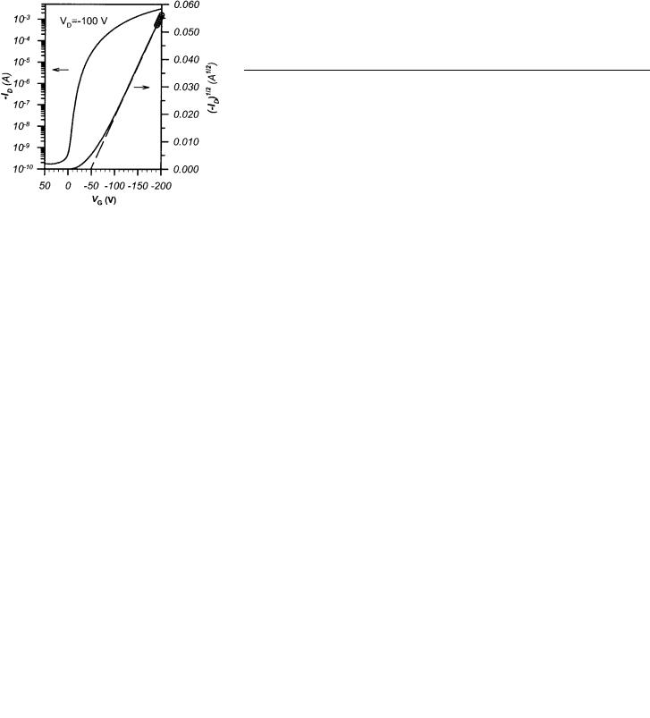
Figure 4 shows a graph that contains a semilogarithmic plot p•••••••••••
of ID versus VG and a plot of j ID j versus VG. It corresponds to a top-contact OTFT with L = 15.4 lm and width W =
p•••••••••••
Fig. 4. Semilogarithmic plot of ID versus VG (left y-axis) and plot of j ID j versus VG (right axis) from a top-contact OTFT comprising a polycrystalline pentacene thin film channel, a 5000 Š thick SiO2 gate insulator layer, a heavily doped n-type Si wafer as the gate, and Au source and drain electrodes. The field-effect mobility l, calculated in the saturation regime, is 1.23 cm2 V±1 s±1 at VD = ±200 V. L = 15.4 lm and W = 500 lm.
500 lm, comprising pentacene as the semiconductor layer, 5000 Š thick thermally grown SiO2 as the gate insulator, heavily doped Si (n-type) as the gate electrode and gold source, and drain electrodes. The field-effect mobility l, calculated in the saturation regime, is 1.23 cm2 V±1 s±1 at VD = ±200 V, while the threshold voltage VT was approximately ±50 V. The Ion/Ioff ratio was above 1.8 ” 107 when VG was
scanned from ±200 to +50 V.[56] It is important to note that W/L must be at least 10 in order to minimize the effects of fringe currents flowing outside the channel, otherwise the mobility is overestimated. Alternatively, accurate mobility measurements could be obtained by patterning the semiconductor such that its width does not exceed the width of the OTFT channel.
Strictly speaking, Equations 1 and 3 are valid only when the mobility is constant. As described below, the mobility in some OTFTs is gate bias dependent. Thus, despite of their widespread use, the above equations should only be used for estimating an approximate value of the field effect mobility in such OTFTs, and mobility values calculated this way should be treated as such. Recently, Horowitz and coworkers have developed and described a procedure for the calculation of gate field dependent mobilities in OTFTs over wide gate volt-
age ranges, meanwhile accounting for the series contact resistance that may exist in these devices.[57,58]
The mobility values of pentacene OTFTs most often
reported in the literature are calculated in the saturation regime.[37,38,55,59] Typically, the mobility calculated in the satu-
ration regime in pentacene OTFTs is much higher than the mobility calculated in the linear regime.[60] The linear regime mobility is more negatively affected by departures from linearity in the ID versus VD curves, at low VD. Gold and other metals with even higher work functions (e.g., Pd, Pt) that are most commonly used for source and drain contacts in p-type OTFTs, form ohmic contacts with pentacene, as expected by comparing gold's work function to the valence band (or highest occupied molecular orbital, HOMO) energy level of pentacene crystals. A proof of this has been provided by comparisons of twoand four-point resistance data from pentacene OTFTs with Au contacts.[43] In addition, hole mobilities from the linear and saturation regimes calculated from single crystal field-effect transistors (FETs) of pentacene, are identical.[31] The origin of large differences between the two mobilities could be the existence of large concentrations of trap states in the channel (e.g., related to grain boundaries).
5. Vacuum Deposited Organic Semiconductor
Films
Organic semiconductor films can be deposited by sublimation in a variety of vacuum deposition systems, utilizing techniques in which the deposition parameters vary widely. OTFTs with good charge carrier transport properties have been fabricated using most of these techniques. The base pressure of the deposition system is an important deposition parameter, since it determines, among other things, the mean free path of the sublimed organic semiconductor molecules, and the presence of unwanted atoms and molecules in the vicinity of the substrate surface during film formation. It ranges from less than 10±9 torr, in ultra high vacuum organic molecular beam deposition (OMBD),[7a] to about 10±7 torr for common high vacuum bell-jar deposition systems, to more
104 |
Ó WILEY-VCH Verlag GmbH, D-69469 Weinheim, 2002 0935-9648/02/0201-0104 |
$ 17.50+.50/0 |
Adv. Mater. 2002, 14, No. 2, January 16 |
C. D. Dimitrakopoulos, P. R. L. Malenfant/Organic Thin Film Transistors
than 10±3 torr for simple, glass-wall vacuum sublimation systems.[61] In addition, organic sublimation systems that employ
a carrier gas to transport the organic molecules from the source to the substrate have also been used.[31±33]
Substrate temperature and deposition rate are two other deposition parameters that can influence dramatically thin
film morphology and thus the transport characteristics of
OTFTs.[50,62]
Purity of the organic source material is also important and together with substrate cleanliness they can determine in large part the quality of an OTFT. The latter is very important since the carrier accumulation layer is occurring in the first
few monolayers of the organic semiconductor at the interface with the insulator.[11,12] Impurities can affect the mobility, the
on/off ratio and in some cases even the polarity of the OTFT.
For example, iodine-doped pentacene is a p-type semiconductor[63] while alkaline metal-doped pentacene is an n-type semi-
conductor.[64]
The synthesis and fabrication of OTFTs based on polycrystalline, vapor deposited 6T[65,66] and a-x-dihexyl-sexithio-
phene[67] films by Garnier et al. played a very important role in the evolution of the field of organic transistors. That work showed not only that relatively high mobilities are attainable by polycrystalline organic semiconductors, but also delineated the strategies that should be followed in order to increase the performance of OTFTs. In the case of chainor rod-like molecules, such as thiophene oligomers, large p-conjugation length along the long axis of the molecule and close molecular packing of the molecules along at least one of the short molecular axes (p-stacking) are two important conditions for high carrier mobility. These principles are also in operation in OTFTs
based on polycrystalline, vapor deposited pentacene thin
films.[31,38,50,59,66]
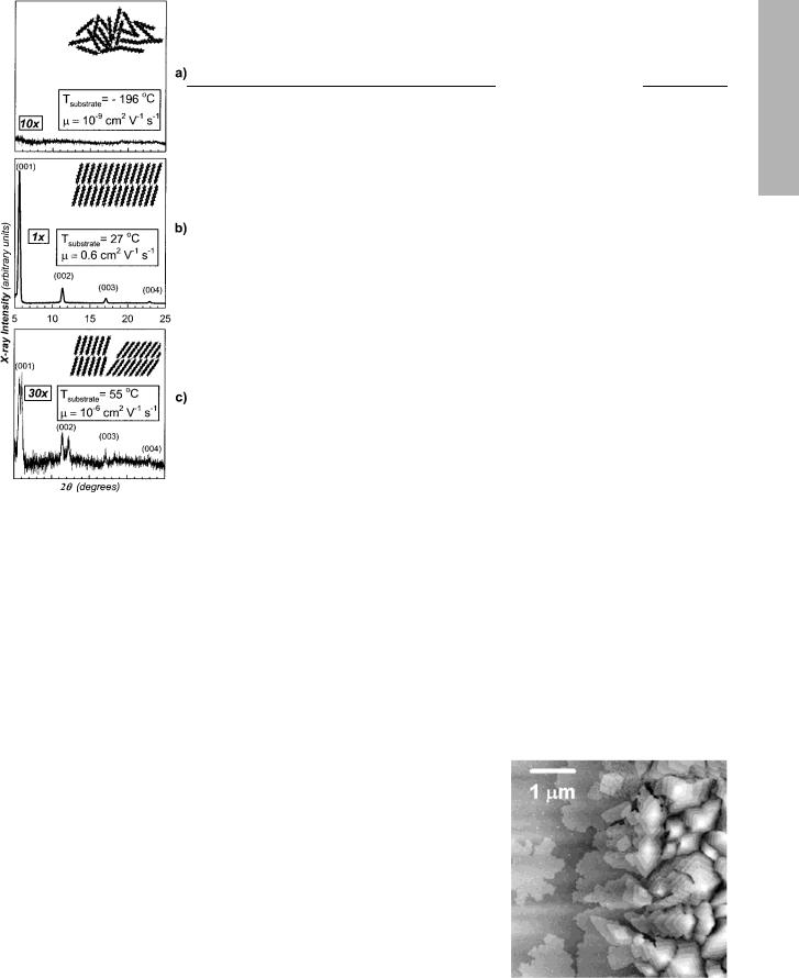
Figure 5[50,68] contains proof of the above claims. By growing amorphous films of pentacene, which is achieved by keeping the substrate temperature close to ±196 C during deposition, a film that is practically insulating is produced. This is due to the fact that the overlap of the molecular orbitals of nn molecules is very limited because of the disorder in the solid (Fig. 5a). When the substrate temperature is kept at RT during deposition, a very highly ordered film is deposited, and the mobility measured at RT is 0.6 cm2 V±1 s±1 (Fig. 5b). The structure of this thin film is different than the structure of sin-
gle crystals of pentacene, thus we must distinguish between the ªthin-film phaseº[50,62] and the ªsingle-crystal phaseº[69] of
pentacene. When a mixture of the thin film phase and the single crystal phase is grown,[50] the mobility is very low, possibly
due to the high defect concentration resulting from the coexistence of the two phases (Fig. 5c).
Figure 6 shows the morphology at the edge of a pentacene film grown on SiO2 at RT through a shadow mask.[53] We
observe that the first layer of pentacene forms single crystal islands with a lateral size of a few micrometers. Subsequent layers growing on top of these islands are smaller in size leading to a terrace-and-step morphology. The angles formed by the sides of some of the uppermost pentacene islands seem to
Fig. 5. X-ray diffractograms, schematic representations of structural order, and field-effect mobilities corresponding to three different thin film pentacenes. a) An amorphous phase is achieved using a substrate temperature, Tsub = ±196 C and a
deposition rate, DR, of 0.5 Š s±1. b) A single ªthin film phaseº [50] resulted for Tsub = 27 C and DR = 1 Š s±1. c) Setting Tsub = 55 C and DR = 0.25 Š s±1 yielded a film consisting of two phases, the ªthin film phaseº and the ªsingle crystal phaseº
[68]. Data is partially taken from [50].
Fig. 6. Morphology at the edge of a pentacene thin film grown at RT on SiO2 through a shadow mask. Reprinted from [53].
be consistentÐat the extent of accuracy that the photograph permitsÐwith the angles of the ab-plane of the triclinic unit cell of pentacene.[69] Recently, photoelectron emission microscopy (PEEM) was employed to study pentacene thin film
REVIEW
Adv. Mater. 2002, 14, No. 2, January 16 |
Ó WILEY-VCH Verlag GmbH, D-69469 Weinheim, 2002 0935-9648/02/0201-0105 |
$ 17.50+.50/0 |
105 |
REVIEW
C. D. Dimitrakopoulos, P. R. L. Malenfant/Organic Thin Film Transistors
growth in real time and the resulting understanding contributed significantly to the identification of the pentacene growth mechanism on various surfaces.[70] Polycrystalline films of pentacene with grain sizes approaching 100 lm were fabricated on clean Si(001) surfaces passivated with a cyclohexene layer.[70] Such large grain growth can be attributed to the relatively low nucleation density of pentacene grains on such surfaces under the conditions used, which is of the order of 10±3 lm±2, and the absence of heterogeneous nucleation on the carefully cleaned Si substrates.[70] However, the nucleation density of pentacene grains onÐthe technologically more important for OTFT applicationsÐSiO2 surface was reported to be 100 times higher than on Si(001) and cyclohexene-modi- fied Si(001) surfaces, under the same deposition parameters.[70] Higher nucleation density generally translates to smaller grain sizes. Notably, Schön et al. have succeeded in depositing polycrystalline pentacene films on polyimide sub-
strates with grain sizes of 100 lm using a substrate temperature below 200 C.[31]
6. Dependence of Mobility on Gate Voltage
Pentacene TFTs have produced the highest performance among TFTs with an organic semiconducting channel (see Table 1). However, the operating voltage required to produce such performance (100 V) is usually too high, especially for portable, battery-powered device applications. We studied the gate voltage dependence of mobility in pentacene devices, and used our understanding to demonstrate high performance pen-
tacene TFTs exhibiting mobility up to 0.4 cm2 V±1 s±1 at low operating voltages (~5 V).[39,71] An example of the dependence
of mobility on VG is shown in Figure 7, which shows plots of
p•••••••••••
mobility and j ID j vs. VG for the device in Figure 4. The mobility is continuously calculated in the saturation regime for various maximum values of VG. Clearly, there is a very strong dependence of mobility on VG. The mobility increases from
very low values (about 0.02 cm2 V±1 s±1 at VG |
= ±14 V) to |
1.26 cm2 V±1 s±1 at ±146 V. At even higher VG |
the mobility |
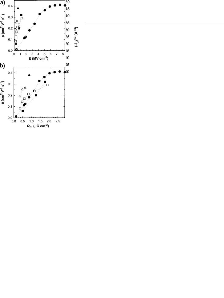
reaches a plateau. The ability to set VG as high as 200 V enabled us to reach this mobility plateau even with an OTFT comprising a relatively thick (5000 Š) SiO2 gate insulator. This had not been possible before. Furthermore, improvements in some of the deposition parameters of the organic semiconductor, which were discussed above have resulted in much higher mobilities in the devices of Figures 3 and 4, relative to earlier pentacene devices with the same gate insulator (see for example the dotted black circles in Figure 8 which correspond to mobilities of 0.012 and 0.124 cm2 V±1 s±1 at VG = 20 and 100 V, respectively). For comparison we note that the mobility measured at maximum gate voltage VG = 20 and 98 V is 0.069 and 1.020 cm2 V±1 s±1, respectively (from Fig. 7).
In order to lower the operating voltage of pentacene OTFTs we have employed gate insulators with a relatively high dielectric constant (e), such as metal oxide films of barium zirconate
Fig. 7. Dependence of field-effect mobility of holes on VG. Plots of mobility p•••••••••••
(left axis) and j ID j (right axis) vs. VG for the device corresponding to Figure 4.
Fig. 8. a) Dependence of field-effect mobility of holes, l, on gate field, E. b) Dependence of l on charge per unit area, QS. Black or white symbols correspond to l calculated from a gate or drain sweep, respectively. See legend for details on gate insulators. 0.5 lm SiO2, gate sweeps (*); 0.12 lm SiO2, gate sweeps (l); 0.082 lm BST, gate sweeps (s); 0.090 lm BST, drain sweeps (~); 0.122 lm BZT, gate sweeps (n); 0.128 lm BZT, drain sweeps (&). The sole purpose of the dotted lines is to guide the reader's eye. Reprinted from [71].
106 |
Ó WILEY-VCH Verlag GmbH, D-69469 Weinheim, 2002 0935-9648/02/0201-0106 |
$ 17.50+.50/0 |
Adv. Mater. 2002, 14, No. 2, January 16 |
C. D. Dimitrakopoulos, P. R. L. Malenfant/Organic Thin Film Transistors
titanate (BZT),[39] or barium strontium titanate (BST)[71] Additionally, we have demonstrated the full compatibility of low operating voltage OTFTs with transparent plastic substrates by making devices on polycarbonate substrates using an all-room- temperature process sequence.[39] It is important to note here that the operating voltage can be reduced by reducing the thickness of the dielectric layer instead of increasing its dielectric constant. However, the fact that the envisioned applications for OTFTs involve almost exclusively large-area electronics, a minimum dielectric layer thickness of 1000 Š or more is dictated by reliability and manufacturing yield considerations. Thicker dielectric layers are more suitable for large area electronics applications since they suppress the formation of pinholes and the problems associated with step coverage. Thus, a higher dielectric constant gate insulator is considered the appropriate solution for high mobility pentacene OTFT with low operating voltage. Later, Gundlach et al. demonstrated
pentacene OTFT devices on plastic with mobility up to 1.1 cm2 V±1 s±1 at operating voltage of about 25 V.[72]
Figures 8a and b show the dependence of field effect mobility, l, on the gate field, E, and the charge per unit area on the semiconductor side of the insulator, QS, respectively.[71] Both E and QS are proportional to VG. The solid black circles correspond to a pentacene-based device with a 1200 Š thick SiO2 gate insulator thermally grown on the surface of a heavily doped n-type Si wafer that acted as the gate electrode. The dotted black circles correspond to a similar device with a 5000 Š thick SiO2 gate insulator. The mobility for the SiO2- based devices is calculated in the saturation regime using a gate sweep, as explained in Figure 4, and is then plotted versus the maximum VG used in each gate sweep. The maximum VG is varied from ±20 to ±100 V. During all sweeps VD is kept constant at ±100 V in order to eliminate any effects that source and drain contact imperfections might have on our results. The mobility increases linearly with increasing QS and E, and eventually saturates (Figs. 8b and a, respectively). QS is a function of the concentration of accumulated carriers in the channel region (N). Since the accumulation region has been shown in the past to be two-dimensional and confined
very close to the interface of the insulator with the organic semiconductor,[11,12] all of this charge is expected to be local-
ized within the first few semiconductor monolayers from this interface. By replacing SiO2 with an insulator having a similar thickness but a much higher dielectric constant, an accumulated carrier concentration similar to the SiO2 case could be attained at much lower VG, and hence E, with all the other parameters being similar. The squares in Figure 8 correspond to devices comprising RT sputtered BZT as the gate insulator. The filled squares are generated by gate sweeps, while the open squares are generated by drain sweeps. From Figure 8a it is obvious that the applied gate field used in BSTand BZTbased devices to obtain mobility values similar to those of the SiO2-based devices was about five times lower compared to the fields used in the latter devices. This clearly proves that high field is not required to obtain high mobility. Thus, the gate voltage dependence of mobility in these devices is due to
the higher concentration of holes accumulated in the channel. Figure 8b, which plots l versus charge per unit area, QS, corroborates this conclusion. The values of QS and N required to reach a certain mobility value are practically the same for SiO2- and BZT-based devices although much different gate voltage and gate field values were required to obtain such a mobility in each case.
The gate voltage dependence of mobility in vacuum deposited pentacene OTFTs was first reported in one of our previous publications.[50] A similar behavior was later reported for pentacene OTFTs deposited from solution via the precursor route (see below).[73] The multiple trapping and release (MTR) model,[74] which is widely used to model the behavior of a-Si:H TFT seems to be a likely mechanism that explains the observed characteristics in vapor deposited polycrystalline films of pentacene. This model, which is based on the assumption that the intrinsic charge transport mechanism is one involving extended states, has been successfully used in the past
to model the field dependence of mobility in 6T and a,x-di- hexyl-sexithiophene (DH6T) OTFTs.[18,39,58,71,75,76] According
to this model a distribution of traps exists in the forbidden gap above the valence band edge. At low gate bias most of the holes injected in the semiconductor are trapped into these localized states. The deepest traps are filled first and carriers can be released thermally. As the negative gate bias increases, the Fermi level approaches the valence band edge as more traps are filled. At an appropriately high voltage all trap states are filled and any subsequently injected carriers move with
the microscopic mobility associated with carriers in the valence band.[39,71] Several trap levels have been reported for
thin polycrystalline vapor deposited films of pentacene at depths ranging from 0.06 eV to 0.68 eV,[77] which could ac-
count for the traps described in the MTR model. Traps can be linked to impurities, and various structural defects in the crystalline structure of the pentacene film, including point defects, dislocations, and most importantly grain boundaries. Schön et al. have used the concept of positively charged grain boundaries to explain the gate voltage dependence of mobility in polycrystalline pentacene films.[31] An energy barrier is created at the grain boundaries and is a function of the charged trapping states at the boundaries, the carrier concentration within the grains and the temperature.[31] The effective mobility across two grains of tetracene that are separated by a grain
boundary is given by: l±1 = lG±1 + lGB±1, where lG is the single crystal mobility (intragrain mobility) and lGB is the mobil-
ity across the grain boundary.[78] The charge transport is dominated by thermionic emission over the potential barrier at the grain boundary from 20 to 150 K, and by the intragrain transport (lG) above 150 K. From 4 to about 20 K transport is dominated by tunneling of charge carriers through the potential barrier at the grain boundary. Chwang and Frisbie have shown that carrier transport in 6T OTFTs is limited by the presence of grain boundaries in the channel.[79] Their experiments involved transport measurements through single grain boundaries in vapor deposited 6T and showed that transport is dependent on carrier concentration exhibiting decreasing
REVIEW
Adv. Mater. 2002, 14, No. 2, January 16 |
Ó WILEY-VCH Verlag GmbH, D-69469 Weinheim, 2002 0935-9648/02/0201-0107 |
$ 17.50+.50/0 |
107 |
REVIEW
C. D. Dimitrakopoulos, P. R. L. Malenfant/Organic Thin Film Transistors
activation energy with increasing carrier concentration. Another important conclusion of that work is that larger threshold voltages in OTFTs correlate with larger trap densities at grain boundaries.[79]
Vissenberg and Matters have studied theoretically the field effect mobility in OTFTs comprising amorphous organic semiconductor channels, and have successfully used percolation theory and the concept of transport by carrier hopping in an exponential density of localized states to model the experimentally
obtained gate voltage and temperature dependence of mobility from such OTFTs.[80] It should be mentioned here that hopping
transport models differ substantially from models like MTR that assume delocalized transport limited by traps or grain boundaries. They showed that the mobility dependence on temperature in such OTFTs exhibits a simple Arrhenius behavior, with a gate voltage dependent activation energy. According to this model, the differences in the magnitude and temperature dependence of the mobility in pentacene and polythienylenevinylene (PTV) transistors are mainly due to differences in the structural order of the organic semiconductor channels.[80]
Yu et al. have proposed a model that successfully explains field and carrier density dependences of the mobility in films of conjugated organics, both in low-field/high carrier concentration cases (OTFTs), and in high-field/low carrier concentration cases (organic diodes). This model is based on the assumptions that thermal fluctuations modify the energy levels of polaronic electronic states, and that the primary restoring force for these fluctuations is steric, which leads to spatial correlation in the energies of the localized electronic states.[81]
Pentacene transistor drain±source contacts can be made in one of two configurations (Figs. 2a and b): top contact and bottom contact. The performance of pentacene devices with the bottom contact configuration is inferior to that of devices with the top contact configuration. Consequently, most highperformance pentacene TFTs reported in the literature have the top contact configuration, and shadow masking is generally used to pattern the source and drain contacts on top of the pentacene. Unfortunately, this is a process that cannot be used in manufacturing, hence a protocol that allows the photolithographic patterning of the source and drain electrodes on the insulator before the deposition of pentacene, according to the schematic shown in Figure 2b, had to be developed. Furthermore, the performance of devices fabricated with such a process should be similar if not better than that of top contact devices (Fig. 2a).
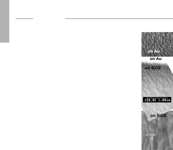
Figure 9 shows a pentacene layer as it was grown on SiO2 and a Au electrode.[82] The edge between SiO2 and Au is
marked by the end of the white in the middle photograph area that corresponds to Au (due to variations in image contrast, the pentacene-covered Au appears different in the top two pictures). On SiO2, far away from the Au edge, pentacene consists of fairly large grains (having sizes between 0.2 and 0.5 lm). On
Au the grain size is dramatically reduced. This small crystal growth persists into the channel region (on SiO2).[82±84] Close
to the Au edge but on the SiO2 side there is a transition region where the grain size increases with increasing distance from
Fig. 9. Scanning electron microscopy (SEM) image of a pentacene thin film grown on SiO2 and a Au electrode. The grain size is much smaller on Au than on SiO2 far from the Au edge. The pentacene grain size on SiO2 in the region close to the Au edge is similar to that on Au and increases with increasing distance from the edge. Reprinted from [82].
the edge. It is the morphology of the pentacene film in the OTFT channel region close to the electrode edge that causes the performance limitation of the bottom contact TFT. Right at the edge of the Au electrode, there is an area with very small crystals and hence a large number of grain boundaries. Grain boundaries are high-volume and low-order regions that contain many morphological defects, which in turn are linked to the creation of charge carrier traps with levels lying in the band-gap. These defects can be considered responsible for the reduced performance of bottom contact pentacene TFTs. The reduction of their concentration to levels similar to those in the area at the center of the channel (lower part of Fig. 9) should result in bottom contact devices with performance similar to or better than that of top contact devices. In a typical bottom contact pentacene TFT the mobility is equal to or less than 0.16 cm2 V±1 s±1. We have used a SAM of 1-hexadecane thiol to modify the surface energy of the Au electrode in an effort to improve the crystal size and ordering of the pentacene overgrowth.[84] Mobilities calculated in saturation from such
108 |
Ó WILEY-VCH Verlag GmbH, D-69469 Weinheim, 2002 0935-9648/02/0201-0108 |
$ 17.50+.50/0 |
Adv. Mater. 2002, 14, No. 2, January 16 |