

nanotechnology / AM1
.PDFC. D. Dimitrakopoulos, P. R. L. Malenfant/Organic Thin Film Transistors
devices were up to 0.48 cm2 V±1 s±1, which is three times larger than the mobility of devices with untreated Au electrodes. Mobilities calculated in the linear regime were up to 5 times higher in devices treated with a SAM vs. untreated devices.[84] The pentacene layers for both devices were deposited in the same deposition run. Figure 10 provides an explanation for the improvement in device performance.[84] The SAM deposited on Au resulted in a pentacene grain size on Au similar to the large grains grown on the SiO2 in the center of the channel.
Fig. 10. SEM image of a pentacene thin film grown on SiO2 and a Au electrode covered with a SAM of 1-hexadecane thiol. A similar grain size on both the SiO2 and the Au/SAM surface is observed. The pentacene grain size transition region at the Au edge is eliminated. Reprinted from [84].
There is no transition region at the Au edge, hence the trap concentration must have been drastically reduced. As described in more detail in the section on n-type OTFTs below, the SAM may have the additional effect of altering the apparent workfunction of the metal electrode relative to the organic semiconductor HOMO and lowest unoccupied molecular orbital (LUMO). This could affect the carrier injection characteristics from the contacts to the organic semiconductor and thus alter the overall performance of OTFTs. However, in the specific case of pentacene OTFTs it has been shown previously that Au forms ohmic contacts to pentacene (see above).[43] Thus the presence of a SAM could only make hole injection less efficient if it shifted the apparent workfunction of Au to lower values compared to an unmodified Au surface. If, on the other hand, it shifted it to higher values, it would not significantly effect hole injection, since the contact of unmodified Au to pentacene is ohmic. Thus, we do not believe that changes in gold's apparent workfunction due to deposition of a SAM play an important role in the improvement of the performance of pentacene OTFTs comprising SAM modified Au source and drain electrodes.
7. Solution Processed Organic Semiconductor
Films
The technology that is believed to have the potential to produce the highest impact on manufacturing costs is the use of soluble organic semiconductors, both polymers and oligomers,
combined with large area stamping or printing techniques that could eliminate lithography. Below, we summarize some important recent developments in this field.
One of the first solution-processable organic semiconductors used for FETs was poly(3-hexylthiophene) or P3HT, in
which the addition of alkyl side-chains enhanced the solubility of the polymer chains.[85] P3HT films spun from a chloroform
solution had mobilities in the range of 10±5 to 10±4 cm2 V±1 s±1. These mobilities were comparable to the mobilities obtained from electrochemically-prepared polythiophene FETs,[86] indicating that the incorporation of insulating alkyl side chains was not detrimental to the electronic properties of polythiophene. A comparison study of poly(3-alkylthiophene)s with side chains ranging in length from butyl to decyl showed that field-effect mobility decreases with increasing chain length.[87] For films spun from chloroform, mobilities ranged from 1±2 ” 10±4 cm2 V±1 s±1 for poly(3-butylthiophene) and P3HT down to
6 ” 10±7 cm2 V±1 s±1 for poly(3-decylthiophene).
When regioregular P3HT[88] consisting of 98.5 % or more head-to-tail (HT) linkages (Scheme 1) was used to fabricate FETs, a dramatic increase in mobility was observed relative to regiorandom poly(3-alkylthiophene)s.[89] Mobilities as high as 0.045 cm2 V±1 s±1 were achieved in films drop-cast from a
Scheme 1. Molecular structures of common p-type organic semiconductors.
chloroform solution.[89] Drop cast films of highly regioregular P3HT self-orient into a well-ordered lamellar structure with an edge-on orientation of the thiophene rings relative to the substrate.[88] This is in contrast to solution cast films of regiorandom poly(3-alkylthiophene)s, which are essentially amorphous.[88] Spin-coated films of regioregular P3HT are
REVIEW
Adv. Mater. 2002, 14, No. 2, January 16 |
Ó WILEY-VCH Verlag GmbH, D-69469 Weinheim, 2002 0935-9648/02/0201-0109 |
$ 17.50+.50/0 |
109 |

REVIEW
C. D. Dimitrakopoulos, P. R. L. Malenfant/Organic Thin Film Transistors
also well ordered, but the lamellae adopt different orientations depending on the degree of regioregularity.[90] Highly regioregular P3HT (greater than 91 % HT linkages) also forms lamellae with an edge-on orientation (p±p stacking direction in the plane of the substrate) when spun from chloroform. Mobilities of 0.05 to 0.1 cm2 V±1 s±1 were obtained for 96 % regioregular P3HT.[90] In contrast, spin-coated films of P3HT with low regioregularity (81 % HT linkages) consisted of lamellae having a face-on orientation (p±p stacking
direction perpendicular to the substrate) and resulted in mobility of 2 ” 10±4 cm2 V±1 s±1. Drop cast films of 81 %
regioregular P3HT adopted an edge-on lamellar structure, resulting in an order-of-magnitude increase in mobility compared to spin-coated films. This study indicates that, in addition to the degree of order in the polymer film, the p±p* stacking direction relative to the substrate, which depends on the film deposition method, greatly affects the field-effect mobility.[90] This is reasonable, since the edge on lamellar structure ensures that delocalized intermolecular states are formed in the direction parallel to the substrate, which happened to be the transport direction in OTFT devices.
The mobility of regioregular P3HT has been found to vary by two orders of magnitude depending on the solvent used, with chloroform giving the highest mobility.[89] Modification of the substrate surface prior to deposition of regioregular poly(3-alkylthiophene) has also been found to influence film morphology. For example, treatment of SiO2 with hexamethyldisilazane (HMDS) or an alkyltrichlorosilane replaces the hydroxyl groups at the SiO2 surface with methyl or alkyl groups. The apolar nature of these groups apparently attracts the hexyl side chains of P3HT, favoring lamellae with an edge-on orientation. Mobilities of 0.05 to 0.1 cm2 V±1 s±1 from
highly regioregular P3HT have been attributed to this surface modification process.[91,92] In addition, it has been shown that
top contact devices yield mobilities that are typically larger by a factor of two compared to bottom contact devices.[91,93]
Exposure of poly(3-alkylthiophene) films to air causes an increase in conductivity and a subsequent degradation of the transistor on/off ratio. This is the result of doping with oxygen (doping by water is a less probable but possible cause), since
it is possible to achieve high on/off ratios by preparing and testing devices in a dry N2 atmosphere.[91,93] Gate induced
superconductivity in a polymer was recently reported in drop cast, bottom contact P3HT TFT, at T £ 2.35 K, and at sheet carrier densities exceeding 2.5 ” 1014 cm±2, demonstrating for the first time that the properties of organic polymers can be tuned from insulating to semiconducting, to metallic and finally to superconducting.[94] Superconductivity had been observed in the past in crystalline inorganic polymers,[95] and one-dimensional stacks of non-polymeric, conducting organic salts such as tetramethyltetraselenafulvalene (TMTSF), which
were the first organic conductors to exhibit superconductivity.[96]
Sirringhaus et al. have recently demonstrated direct inkjet printing of OTFTs based on solution-processed polymer electrodes (water-soluble poly[3,4-ethylenedioxythiophene]
doped with polystyrene sulfonic acid (PEDOT/PSS)), insulators (polyimide), and active organic semiconducting layer (poly[9,9-dioctylfluorene-co-bithiophene], called F8T2, from xylene solution).[97] It was shown that F8T2, which is a nematic liquid crystalline conjugated polymer semiconductor, can be preferentially oriented by rubbed polyimide layers,
and when used as the active channel in OTFTs it exhibits a mobility of 0.02 cm2 V±1 s±1 and an on/off ratio of 105.[97,98]
While spin coating, solution casting and printing are perhaps the most commercially feasible processing techniques for soluble polymeric semiconductors, the Langmuir±Blodgett
(LB) technique and its variations have also been explored for the preparation of poly(3-alkylthiophene) FETs.[99±102] The
maximum mobility measured from multilayer LB films of P3HT was 0.02 cm2 V±1 s±1.[101]
Unsubstituted quinquethiophene and end-substituted qua- ter-, quinque-, and sexithiophene display enough solubility in organic solvents to allow fabrication of field-effect devices by solution processing techniques. Initial studies of solutionprocessed oligothiophene transistors gave mobilities of ~5 ” 10±5 cm2 V±1 s±1 for quinquethiophene and a,a¢-diethylqua- terthiophene (DE4T).[103] More recently, mobilities in the
range of 0.01 to 0.1 cm2 V±1 s±1 have been achieved using solution processed substituted oligothiophenes.[104±107] The mobil-
ity was found to depend strongly on film morphology, which can be controlled by processing conditions, such as solution concentration, substrate temperature during casting, solvent choice, and environmental conditions during film drying.
Other soluble organic oligomers have also been investigated as semiconducting materials for FETs. Anthradithiophene, a fused heterocycle compound, is soluble in its dihexyl end-substituted form. Dihexylanthradithiophene (DHADT) transistors were fabricated by solution casting from hot chlorobenzene, followed by evaporation of the solvent in a vacuum oven at various temperatures. The electrical characteristics of the films were strongly dependent on the temperature during film drying. The highest mobilities, 0.01 to
0.02 cm2 V±1 s±1, were obtained for a drying temperature of 100 C.[106,108] In comparison, vacuum evaporated films of DHADT gave mobilities as high as 0.15 cm2 V±1 s±1.[108]
Transistors utilizing another thiophene-containing oligomer, trans±trans-2,5-bis[2-{5-(2,2¢-bithienyl)}ethenyl]thiophene (BTET), were fabricated by spin coating from hot N-methyl
pyrrolidinone (NMP). The mobility of such a device was 1.4 ” 10±3 cm2 V±1 s±1 compared to 0.012 cm2 V±1 s±1 for a vacuum
evaporated device.[109]
Although a great deal of success has been achieved with soluble oligomers, the solubility of these oligomers is low, requiring the solvents to be heated. Drop casting and spinning yield films that are non-uniform in thickness, morphology, and electrical properties. To circumvent such problems, another approach to solution processable oligomeric materials has been developed that involves a soluble precursor molecule that is not semiconducting, and which can be converted to its semiconducting insoluble form upon heating. This approach has been realized for pentacene, with initial reported mobili-
110 |
Ó WILEY-VCH Verlag GmbH, D-69469 Weinheim, 2002 0935-9648/02/0201-0110 |
$ 17.50+.50/0 |
Adv. Mater. 2002, 14, No. 2, January 16 |

C. D. Dimitrakopoulos, P. R. L. Malenfant/Organic Thin Film Transistors
ties of 0.01 to 0.03 cm2 V±1 s±1.[16,110,111] The pentacene precursor is soluble in dichloromethane and forms continuous, amorphous films when spun onto substrates. The conversion to pentacene is accomplished by heating the films to a temperature of 140±220 C in vacuum. Tetrachlorobenzene is eliminated in the conversion process. In a more recent study, a mobility of 0.2 cm2 V±1 s±1 was achieved by treatment of the SiO2 substrate with HMDS prior to spin coating the precursor, and by optimizing the conversion conditions. Precursor films were formed by spin coating from a 1.5 wt.-% solution
in dichloromethane, and heating the film for 5 s at 200 C followed by rapid quenching.[112]
The precursor approach has also been applied to polymers. In fact, one of the first reported transistors based on organic
polymer channels used precursor-route polyacetylene as the semiconducting layer.[113,114] Another polymeric semiconduc-
tor that has been processed from a soluble precursor polymer
is PTV.[16,30,86,111]
8. N-Type Organic Semiconductors
High performance n-type materials will enable the fabrication of p±n junctions, as well as complementary logic circuits. It's interesting to note that most of the work to date has focused on p-type organic materials such as pentacene, poly(3- alkylthiophene), or oligothiophenes, which were described in the previous section, whereas only recently has any serious effort been guided towards the preparation of novel n-type semiconductor materials. The disproportionate development of p-type organic FETS (OFETs) vs. n-type is clearly the result of the inherent instability of organic anions, in particular carbanions, that react with oxygen and water under operating conditions, thus providing unstable devices.
De Leeuw et al. have indirectly addressed this issue by examining the stability of n-type doped (i.e., reduced) poly-
mers and by evaluating standard redox potentials for reactions with water and oxygen.[115] He concluded that although
there is an optimum thermodynamic stability window that can be determined based on standard redox potentials, the stability of n-type doped materials depends strongly on the value of the overpotential (i.e., free energy of activation) associated with the chemical processes (i.e., reaction with either water or oxygen).[116] Therefore, careful tuning of the electron affinity of n-type materials will have to be done in order to obtain thermodynamically stable devices, otherwise passivating layers or encapsulants will have to be employed. Alternatively, air stability could be achieved by kinetically inhibiting the undesired redox processes. For instance, the incorporation of hydrophobic functionalities into the chemical structure of the organic semiconductor could prevent the penetration of water, thus providing a ªkineticº barrier.
Design rules for n-type organic semiconductors are very similar to p-type materials except that n-type devices must utilize semiconductor materials that allow the injection of electrons into its LUMO. Therefore, the electron affinity of the semicon-
ductor should be optimized such that the LUMO level (conduction band) offset with respect to the Fermi level of the source and drain electrodes does not limit the injection of electrons from the source into the semiconductor and from the semiconductor into the drain. Most of the work done to date has employed gold electrodes as the source and drain. Gold has a work function of ~5.0 eV against vacuum and since most n-type materials have solid state electron affinity levels ~4.0 eV, this energy barrier of approximately 1 eV would be expected to severely limit charge injection into the semiconductor. Interestingly, this is not the case. What is known is that when gold surfaces are coated with organic materials, the apparent workfunction of the metal can change by up to 1 eV, thus facilitating the injection of charge into n-type materials.[117] Alternatively, this apparent workfunction change can be interpreted in terms of an ultrathin, interfacial electric dipole layer that in effect results in a vacuum level shift at the metal/organic interface.[118] This phenomenon ultimately introduces another element of complexity in terms of attempting to match the workfunction of the electrodes with the intended semiconductor conduction band in order to produce ohmic contacts.
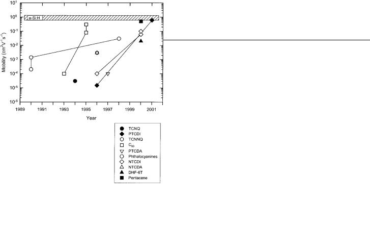
The literature on n-type OTFTs takes us back only 10 years. Table 2 lists the highest field-effect mobility (l) values measured from n-type OTFTs as reported in the literature, annually from 1990 to the present time, for each one of the
Table 2. The highest field-effect mobility (l) values measured from n-type OTFTs as reported in the literature, annually from 1990 to the present time, for each one of the most promising n-type organic semiconductors.
[a] On/off ratio increases upon exposure to air. [b] Personal communication.
most promising n-type organic semiconductors. Figure 11 graphically conveys the information contained in Table 2. The various n-type materials are grouped together, when possible, taking into consideration only the core part of each molecule and not the specific substituents.
Early work in this area provided some devices with respectable mobilities and on/off ratios yet they were unstable in air. Some materials provided devices with limited air stability but charge transport properties were poor and none of these materials were soluble enough to be processed from solution.
REVIEW
Adv. Mater. 2002, 14, No. 2, January 16 |
Ó WILEY-VCH Verlag GmbH, D-69469 Weinheim, 2002 0935-9648/02/0201-0111 |
$ 17.50+.50/0 |
111 |
REVIEW
C. D. Dimitrakopoulos, P. R. L. Malenfant/Organic Thin Film Transistors
Fig. 11. Evolution of OTFT mobility for the most common n-type organic semiconductors. The various n-type materials are grouped together into families of similar molecules taking into account only the core part of each molecule. For reference, a representative range of electron mobilities for a-Si:H TFT is shown.
Recently, researchers have been able to obtain materials that provide devices with most of the requisite properties such as high mobility and current on/off ratio as well as stable operation in air, and solution processability. The remainder of this review is intended to summarize the area of n-type OTFTs by focusing on charge transport characteristics as well as the effect of deposition conditions on morphology and device performance. The organization is for the most part chronological, while individual sections are distinguished by the basic chemical structure of the semiconductor materials used for OTFT fabrication.
The earliest study on n-type OTFTs was undertaken by Guillaud and co-workers and involved lutetium (Pc2Lu) and thulium (Pc2Tm) bisphthalocyanines.[119] Device stability is excellent under vacuum at RT, therefore electrical measurements were made in situ, without breaking vacuum at any point in time during the process of fabrication. N-type mobilities of 10±3±10±4 for both Pc2Tm and Pc2Lu were obtained in vacuo. Interestingly, upon exposure to air, only p-type activity was observed.
Brown and co-workers have explored the use of tetracyano-
quinodimethane (TCNQ) as the active material in an n-type OTFT.[120] Bottom contact devices were fabricated with gold
electrodes. TCNQ has a reduction potential of +0.19 V versus the standard calomel electrode. This is in the same region as the oxidation of p-type materials that are known to make ohmic contacts with gold. Hence, the LUMO level of TCNQ is expected to be in the vicinity of the Fermi level of the gold contacts, thus allowing for facile electron injection into
TCNQ. Nevertheless, very poor devices provided a mobility of 3 ” 10±5 cm2 V±1 s±1 and an on/off ratio up to 450 upon expo-
sure to air (4 to 450).
Haddon et al. have explored the use of C60 as the semiconducting material in n-type FET devices.[121] C60 films were
deposited under ultra high vacuum (UHV) such that no exposure to oxygen occurred. Such films consist of random polycrystalline grains of approximately 60 Š in size. Chromium and gold electrodes were used. In separate experiments it was shown that Cr electrodes lead to higher conductivities and create more carriers at the C60/Cr interface than Au/Cr double layers. C60 devices are sensitive to amine exposure and pretreatment of the substrate with tetrakis(dimethylamino)ethylene (TDAE) prior to deposition of C60 moves the threshold voltage to negative values (the device does not turn off at 0 V) and increases the FET mobility by a factor of 3
(l = 0.08 to 0.3 cm2 V±1 s±1) at the expense of the current on/off ratio. It has been shown in previous work[122] that C60
can be reduced by TDAE, thus doping is likely to be the cause of the increase in mobility and concomitantly the increase in off-current.
Unfortunately, C60 devices could not be operated in air. Their resistivity quickly increased 4±5 orders of magnitude. Their operation could be restored upon placing the devices in a UHV chamber at elevated temperature overnight. This sug-
gests that oxygen acts as electron traps within the C60 lattice. TOF measurements for C60 single crystals[123] have shown
mobilities of 0.5 cm2 V±1 s±1, thus, as expected from the discussion in a previous section, the grain boundaries lower the mobility in thin evaporated films. Isotropic films of C60 provide good device characteristics, in contrast to other materials that require special consideration in order to obtain highly ordered structures. This may be related to the approximately spherical shape of C60 as opposed to the rigid rod shape or more generally elongated shape of most of the other organic semiconductors.
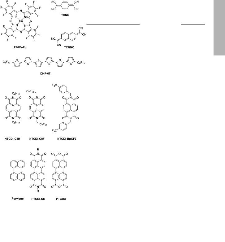
Katz and co-workers have explored several materials based on the naphthalene framework (see Scheme 2).[104,124] Initially
explored was 1,4,5,8-naphthalene tetracarboxylic dianhydride (NTCDA) in which mobilities of 1±3 ” 10±3 cm2 V±1 s±1 were measured for materials deposited onto substrates held at 55 C. Upon exposure to air the mobility decreases by 1±2 orders of magnitude. Lower mobilities are observed when devices are exposed to atmospheric moisture after sublimation. At substrate temperatures of 25 C mobilities of 10±4 cm2 V±1 s±1 were observed. Although similar grain sizes (200 nm) are obtained for both temperatures, films deposited at 55 C were more continuous. Devices constructed from 1,4,5,8-naphthalene tetracarboxylic diimide (NTCDI) provided mobilities on the order of 10±4 cm2 V±1 s±1. Lastly, 11,11,12,12-tetracyanonaphtho-2,6-quinodimethane
(TCNNQ) devices display higher mobilities (10±3) than TCNQ[120] (vide infra), while having better air-stability than
NTCDA. Unfortunately, a high off current is observed, presumably due to unintentional doping, thus providing devices with poor on/off ratios.
112 |
Ó WILEY-VCH Verlag GmbH, D-69469 Weinheim, 2002 0935-9648/02/0201-0112 |
$ 17.50+.50/0 |
Adv. Mater. 2002, 14, No. 2, January 16 |
C. D. Dimitrakopoulos, P. R. L. Malenfant/Organic Thin Film Transistors
Scheme 2. Molecular structures of common n-type organic semiconductors.
Recently, Katz and co-workers reported the fabrication of n-type OTFTs comprising a series of materials based on N,N¢- dialkyl-naphthalene-1,4,5,8-tetracarboxylic diimide (see Scheme 2).[125] In this study, the transport characteristics varied greatly with substitution. For instance, only the fluorinated materials (NTCDI-C8F, NTCDI-BnCF3) showed high mobilities in air, whereas mobilities of 0.001±0.1 were found for linear, alkyl functionalized diimides (NTCDI-C8H, NTCDIC12H, NTCDI-C18H), but only under vacuum. The highest mobility in air (>0.1 cm2 V±1 s±1) was obtained with NTCDIBnCF3, while the highest on/off ratio in air (>105) was achieved with NTCDI-C8F. As observed with many other
organic semiconductors, mobilities were generally much higher when the material was deposited onto a substrate at elevated temperature. Alternative electrodes were examined and carbon electrodes gave similar results to gold electrodes yet not as reproducible. Furthermore, carbon could be used in a bottom contact configuration where as gold generally failed even if cleaned with oxygen plasma. Interestingly, aluminum electrodes did not provide active devices. Although this is likely due to oxidation of aluminum, it is important to note that organic films on low workfunction metals can also alter the effective workfunction, in this case increasing it, thus making it less favorable for injection.[117] Since bottom contact devices rarely produced transistor activity, the use of thiols to modify the gold surface was explored. Excellent results were obtained using 3,4-dichlorobenzyl mercaptan. Currents as high as 100 lA were observed for NTCDI-BnCF3, providing a mobility of ca. 0.1 cm2 V±1 s±1 for bottom contact devices (Tdep = 90±100 C). It has been shown that functionalizing the
surface of gold with thiols can result in a modified work function,[117] yet the presence of an organic monolayer may also
facilitate the ordering of the semiconductor upon deposition, such that the grain boundaries are reduced at the channel/ electrode interface as previously seen with pentacene devices (vide supra). NTCDI-C8F is soluble in hot a,a,a-trifluorotol- uene, and solution casting results in morphologically non-uni- form films, with some regions of the films giving mobilities greater than 0.01 cm2 V±1 s±1.
The gate voltage could be cycled in air for up to 1 h as long as the voltage remained below 50 V. Interestingly, the redox data does not show a significant difference between fluorinated and non-fluorinated derivatives, yet there is clearly a difference in their performance in air. Also, the potentials
measured are formally outside the stability window described by de Leeuw,[115] thus indicating that air stability can be
obtained even with materials that are expected to be unstable thermodynamically. Since thin film orientation and layer spacings are similar for fluorinated and non-fluorinated analogs, solid-state structural characteristics were examined.[126] In the case of the linear side-chains, the dense packing of the fluorinated side-chains (e.g., NTCDI-C8F) vs. aliphatic side-chains (e.g., NTCDI-C8H) could provide a ªkineticº barrier to atmospheric contaminants. Consistent with this hypothesis, is the relatively lower stability of the less densely packed NTCDI-BnCF3 derivative vs. NTCDI-C8F, yet such an argument is not so straight forward when comparing NTCDIBnCF3 to NTCDI-BnCH3, in which the former provides air stable devices yet the later has mobilities on the order of 10±5 cm2 V±1 s±1 even under vacuum. It is also interesting to note the dramatic stability difference observed between single crystals of NTCDI-BnCF3 and NTCDI-BnCH3. The subtle packing differences in the single crystal may account for the significantly lower activation energy required to fill trapping levels in the NTCDI-BnCF3 derivative, thus providing better device performance. Clearly, similar film morphologies do not extrapolate to comparable device performance such as mobility and current on/off ratios.
REVIEW
Adv. Mater. 2002, 14, No. 2, January 16 |
Ó WILEY-VCH Verlag GmbH, D-69469 Weinheim, 2002 0935-9648/02/0201-0113 |
$ 17.50+.50/0 |
113 |

REVIEW
C. D. Dimitrakopoulos, P. R. L. Malenfant/Organic Thin Film Transistors
Garnier and co-workers have explored the n-type charge carrier characteristics of N,N¢-diphenyl-3,4,9,10 perylenetetra-
carboxylic diimide (PTCDI-Ph) where an electron mobility of 1.5 ” 10±5 cm2 V±1 s±1 was measured.[127] Gold and aluminum
contacts were used in a bottom contact configuration, yet aluminum electrodes were found to have 3 times lower performance. Devices degraded rapidly in air and the field effect was lost after two to three days with gold devices, and even faster with aluminum. Faster degradation of the aluminum devices is most likely due to the compounded effect of oxidation at the electrodes as well as the incorporation of moisture and/or oxygen into the film.
Studies with 3,4,9,10-perylenetetracarboxylic dianhydride (PTCDA) also produced devices with poor transport character-
istics where mobilities of 10±4±10±5 cm2 V±1 s±1 were obtained.[128] It is important to note that the orientation of
PTCDA on a surface depends strongly on the deposition conditions used.[129] Films of PTCDA grown on gold were found to
grow quasiepitaxially under specific conditions, thus resulting in highly ordered films.[130] Such low mobilities are ascribed to limited electronic orbital overlap in the direction of transport. Furthermore, PTCDA OTFTs do not operate in wet air, yet in vacuo or under dry oxygen they perform as described previously (vide supra) and the effect of moisture on the devices is reversible. Karl and Marktanner have shown using TOF experiments that the electron mobility in polycrystalline thin
films PTCDA is inversely proportional to the width of the X-ray rocking curve from the thin film.[131,132] The maximum mobility reported was 3 ” 10±2 cm2 V±1 s±1.[131,132]
In a recent study, Schön et al. demonstrated the feasibility of
using a perylene single crystal as the active material in an OFET device.[133] Mobilities of 5.5 cm2 V±1 s±1 were measured at RT.
At low temperatures, mobilities as high as 120 cm2 V±1 s±1 were observed. Such mobilities are in agreement with mobility val-
ues reported from measurements along the b-axis of the perylene monoclinic unit cell.[44,48] As previously described for
members of the acene family (e.g., pentacene electron mobility by inversion at RT is 0.5 cm2 V±1 s±1),[36] perylene is also ambi-
polar, having a hole mobility of 0.4 cm2 V±1 s±1 at RT and 100 cm2 V±1 s±1 at lower temperatures. A RT electron mobility of 5.5 cm2 V±1 s±1 provides a new ceiling value to attain for novel n-type materials.
More recently, Sudhölter and co-workers reported on the liquid crystalline and charge transport properties of three N,N¢-dialkylated, perylene diimides.[134] In particular, N,N¢- dioctadecyl-3,4,9,10-perylenetetracarboxylic diimide (PTCDIC18) demonstrated several crystalline and liquid crystalline phases, consistent with X-ray diffraction experiments that show a high degree of order in all three dimensions. X-ray experiments on the liquid crystal (LC) phases suggest smectic ordering, which is consistent with theoretical models, in which extensive interdigitation of the linear alkyl chains is assumed. Charge carrier mobilities were assessed by pulse-radiolysis time-resolved microwave conductivity and values >0.1 cm2 V±1 s±1 were measured for LC phases and >0.2 cm2 V±1 s±1 for crystalline phases.
We have recently shown that OTFTs based on N,N¢-dioctyl- 3,4,9,10-perylenetetracarboxylic diimide (PTCDI-C8) as the organic semiconductor provides bottom contact devices with mobilities as high as 0.6 cm2 V±1 s±1 in the saturation regime and current on/off ratios >105.[61] High threshold voltages (ca. 75 V) were observed and are attributed to the formation of traps related to structural defects close to the metal contacts, in addition to band offsets.[117] X-ray studies in reflection mode revealed a (001) peak at ca. 20 Š, which is consistent with modeling studies that predict 21 Š, based on extensively interdigitated alkyl chains. This is consistent with the expected smectic ordering observed by Sudhölter (vide supra).
Although historically, metallophthalocyanines have been examined as p-type,[135] appropriate substitution can allow for
the fine tuning of the HOMO±LUMO levels thus altering the majority charge carrier of the material.[136] For example, the work of Bao et al. explored a variety of metallophthalocyanines as channels in n-type OTFTs.[137] Chemical functionality, substrate temperature during the deposition as well as the metal center used were all critical to device performance. Optimum results were obtained with a perfluorinated phtha-
locyanine having M = Cu (F16CuPc) and Tdep = 125 C. It is interesting to note that the effect of fluorinating the rings
results in a 1.6 eV drop in the LUMO level, as assessed by ultraviolet photoelectron spectroscopy (UPS) measurements and ultraviolet-visible (UV-vis) data, thus clearly indicating the advantageous effect of functionalizing materials with electron withdrawing groups for n-type applications. This approach presents an interesting design rule in which known p-type materials can be converted to n-type materials by simply lowering the LUMO levels via substitution with strong electron withdrawing groups. This is analogous to functionalizing naphthalene or perylene with electron withdrawing
diimide moieties. A mobility of 3 ” 10±2 cm2 V±1 s±1 and on/off ratio in the range of 104±105 was obtained for F16CuPc.[137]
Furthermore, these devices could be stored in air for half a year and showed no decrease in mobility or on/off ratio. The edge on stacking of the molecules, effectively resulting in a fluorinated barrier at the surface, could be contributing to the unusual air stability observed in these devices, effectively providing a kinetic barrier as observed with NTCDI-C8F (vide supra).
More recently, Schön et al. studied the electron transport in single crystals of F16CuPc in air as a function of time and temperature.[138] Space charge limited current (SCLC) spectroscopy was used to estimate the intrinsic mobility in single crystals. Charge transport was measured in the p-stacking direction for both single crystals and thin films, in order to eliminate the effect of transport anisotropy, while focusing on the effect of grain boundaries, disorder and other extrinsic parameters. Mobilities as high as 1.7 cm2 V±1 s±1 at RT were estimated for the trap-free SCLC regime. At low temperatures (below 100± 150 K) the effective mobility is dominated by trapping and thus it is thermally activated, whereas at higher temperatures, the effective mobility follows a power law dependence suggesting that band-like transport that is limited by phonon scat-
114 |
Ó WILEY-VCH Verlag GmbH, D-69469 Weinheim, 2002 0935-9648/02/0201-0114 |
$ 17.50+.50/0 |
Adv. Mater. 2002, 14, No. 2, January 16 |

C. D. Dimitrakopoulos, P. R. L. Malenfant/Organic Thin Film Transistors
tering is the dominant mechanism. This observation is analogous to what is observed with perylene single crystals.[47,48,132]
This is in contrast to what is observed with thin films, in which thermally activated transport over a barrier related to grain boundaries is the dominant transport mechanism as described in a previous section. Studies on single crystals in air revealed that the mobility reaches stability after ca. 500 h. Annealing the crystals in the presence of hydrogen provides the original mobility. Thin films, prepared by thermal evaporation onto 125 C substrates were also examined. The FET mobility is temperature independent at low temperature where tunneling becomes the dominant transport mechanism whereas it is thermally activated at higher temperatures. In conclusion, the intrinsic mobility is said to be band-like in a wide temperature range due to the temperature dependence of the mobility for single crystals, whereas polycrystalline films have their charge transport dominated by grain boundary effects.
Recently, Facchetti et al. reported on the use of a,x-diper- fluorohexylsexithiophene (DHF-6T) as a novel n-type organic semiconductor.[139] Once again, a known p-type material (i.e., DH6T) was converted to n-type by simply functionalizing it with appropriate electron withdrawing groups. Although the HOMO±LUMO gap remains the same for both DHF-6T and DH6T (ca. 2.4 eV), redox studies reveal an anodic shift of ca. +0.27 V, thus significantly increasing the ionization potential of DHF-6T and providing a LUMO level ca. 0.27 V below that of DH6T. This result is analogous to what was described for F16CuPc (vide supra). Elevated substrate temperatures were shown to produce grains with larger dimensions and the use of a surface pretreated with 1-(trichlorosilyl)-1,1,2,2-tetra- hydroperfluorooctane (TPFO) led to ca. 10 % increase in crystallite size. More importantly grain±grain and grain±substrate gaps were considerably smaller. Top contact devices were prepared by pre-treating SiO2 surfaces with either HMDS or TPFO prior to the deposition of DHF-6T due to the hydrophilic nature of the oxide. Under a nitrogen atmosphere, mobilities of 0.02 cm2 V±1 s±1 and a current on/off ratio of 105 were obtained in the saturation regime using gold electrodes. Similar results were obtained with aluminum electrodes. Air stability was not addressed. These devices were obtained via depositions where the substrate temperature was 80±100 C. Alternatively, mobilities of 10±4 were obtained when the temperature was ca. 50 C or 120 C. It is interesting to note that the turn-on voltage increases with time, thus resulting in a decrease in on current, yet the turn-on voltage can be stabilized and reduced by post film growth annealing.
In summary, great progress has been achieved with n-type OTFTs over the last 10 years. Mobilities ranging from 0.001± 0.6 cm2 V±1 s±1 and current on/off ratio >105 have been achieved and in some cases air stable devices have been realized.
9. Conclusions
There has been tremendous progress in OTFT performance during the last decade. Our understanding of the properties
and OTFT device operation has improved dramatically. Advances in device performance characteristics have resulted from the introduction of novel materials either obtained by chemical modification of existing ones or by the synthesis of completely new structures, followed by optimization of their morphology and structural order.
At present, we have reached the point at which an initial product application can be seriously considered. Organic semiconductors, such as pentacene, deposited by vacuum-sub- limation remain the best performers due to not only their molecular electronic properties but also their very well ordered films, which result from the use of this highly controllable deposition method. However, substantial improvements have taken place in solution-processed organic semiconductors too, and their mobilities are currently only one order of magnitude lower than those of vapor-deposited pentacene TFTs. There is a potentially important cost-advantage associated with the solution processing of organic TFTs, as it eliminates the need for expensive vacuum chambers and lengthy pump-down cycles. However, for this advantage to be realized, all or at least most of the layers comprising the TFT device should be deposited using methods that do not involve vacuum deposition. These layers include the source, drain, and gate electrodes that currently are made of high work function metals, the gate dielectric, and the (potentially necessary for some materials) passivation/encapsulation layer. Reel-to-reel processing, which has obvious advantages over batch fabrication processes for reducing costs, can be applied to both vacuumand solution-deposited organic semiconductors; thus it does not constitute an exclusive advantage for either of the two classes of materials. If, however, one takes into account the ability to stamp or print solution based organics, thus eliminating traditional lithographic steps, then their potential cost advantage over vacuum deposited organics is apparent. Good device stability and long lifetimes are also required in order to fully realize the benefits of organic electronics. The future looks promising for inexpensive organic electronics as new and improved materials with unique electronic properties are being introduced and integrated into functional devices.
Received: August 10, 2001
Final version: October 31, 2001
±
[1]M. Pope, C. E. Swenberg, Electronic Processes in Organic Crystals and Polymers, 2nd ed., Oxford University Press, Oxford 1999, pp. 337±340.
[2]C. W. Tang, S. A. Van Slyke, Appl. Phys. Lett. 1987, 51, 913.
[3]J. H. Burroughes, D. D. Bradley, A. R. Brown, R. N. Marks, K. Mackay, R. H. Friend, P. L. Burn, A. B. Holmes, Nature 1990, 347, 539.
[4]F. Ebisawa, T. Kurokawa, S. Nara, J. Appl. Phys. 1983, 54, 3255.
[5]K. Kudo, M. Yamashina, T. Moriizumi, Jpn. J. Appl. Phys 1984, 23, 130.
[6]A. Tsumura, H. Koezuka, T. Ando, Appl. Phys. Lett. 1986, 49, 1210.
[7]For previously published graphs of device performance vs. year reported
see: a) C. D. Dimitrakopoulos, B. K. Furman, T. Graham, S. Hegde, S. Purushothaman, Synth. Met. 1998, 92, 47. b) A. Hellemans, Science 1999, 283, 771.
[8]R. H. Friend, J. Burroughes, T. Shimoda, Phys. World 1999, 12, 35.
[9]S. Forrest, MRS Bull. 2001, February, 108.
[10]G. Yu, A. J. Heeger, in Proceedings of 23rd International Conference on the Physics of Semiconductors, Vol. 1 (Eds: M. Scheffler, R. Zimmerman), World Scientific, Singapore 1996, p. 35.
REVIEW
Adv. Mater. 2002, 14, No. 2, January 16 |
Ó WILEY-VCH Verlag GmbH, D-69469 Weinheim, 2002 0935-9648/02/0201-0115 |
$ 17.50+.50/0 |
115 |

REVIEW
C. D. Dimitrakopoulos, P. R. L. Malenfant/Organic Thin Film Transistors
[11]P. Ostoja, S. Guerri, S. Rossini, M. Servidori, C. Taliani, R. Zamboni,
Synth. Met. 1993, 54, 447.
[12]A. Dodabalapur, L. Torsi, H. E. Katz, Science 1995, 268, 270.
[13]N. Greenham, R. H. Friend, in Solid State Physics; Advances in Research and Applications, Vol. 49 (Eds: H. Ehrenreich, F. Spaepen), Academic, San Diego, CA 1995, pp. 1±149.
[14]A. J. Lovinger, L. J. Rothberg, J. Mater. Res. 1996, 11, 1581.
[15]H. E. Katz, J. Mater. Chem. 1997, 7, 369.
[16]A. R. Brown, C. P. Jarrett, D. M. de Leeuw, M. Matters, Synth. Met. 1997, 88, 37.
[17]F. Garnier, Chem. Phys. 1998, 227, 253.
[18]G. Horowitz, Adv. Mater. 1998, 10, 3.
[19]H. E. Katz, Z. Bao, J. Phys. Chem. B 2000, 104, 671.
[20]Carbon Nanotubes: Synthesis, Structure, Properties, and Applications (Eds: M. Dresselhaus, G. Dresselhaus, P. Avouris), Springer, Berlin 2001.
[21]C. Joachim, J. K. Gimzewski, A. Aviram, Nature 2000, 408, 541.
[22]C. Dekker, Phys. Today 1999, 52, 22.
[23]J. M. Tour, Acc. Chem. Res. 2000, 33, 791.
[24] a) P. G. Collins, M. R. Arnold, P. Avouris, Science 2001, 292, 706. b) R. Martel, T. Schmidt, H. R. Shea, T. Hertel, P. Avouris, Appl. Phys. Lett. 1998, 73, 2447.
[25]Y. Taur, T. H. Ning, Fundamentals of Modern VLSI Devices, Cambridge University Press, Cambridge 1998, p. 11.
[26]R. Wisnieff, Nature 1998, 394, 225.
[27]B. Comiskey, J. D. Albert, H. Yoshizawa, J. Jacobson, Nature 1998, 394, 253.
[28]N. K. Sheridon, US Patent 4 126 854, 1978.
[29]B. Crone, A. Dodabalapur, A. Gelperin, L. Torsi, H. E. Katz, A. J. Lovinger, Z. Bao, Appl. Phys. Lett. 2001, 78, 2229.
[30]C. J. Drury, C. M. J. Mutsaers, C. M. Hart, M. Matters, D. M. de Leeuw,
Appl. Phys. Lett. 1998, 73, 108.
[31]J. H. Schön, C. Kloc, B. Batlogg, Org. Electron. 2000, 1, 57.
[32] P. E. Burrows, S. R. Forrest, L. S. Sapochak, J. Schwartz, P. Fenter,
T.Buma, V. S. Ban, J. L. Forrest, J. Cryst. Growth 1995, 156, 91.
[33]M. Baldo, M. Deutsch, P. Burrows, H. Gossenberger, M. Gerstenberg,
V.Ban, S. Forrest, Adv. Mater. 1998, 10, 1505.
[34]C. Kloc, P. G. Simpkins, T. Siegrist, R. A. Laudise, J. Cryst. Growth 1997, 182, 416.
[35]R. A. Laudise, C. Kloc, P. G. Simpkins, T. Siegrist, J. Cryst. Growth 1998, 187, 449.
[36]J. H. Schön, S. Berg, C. Kloc, B. Batlogg, Science 2000, 287, 1022.
[37]S. F. Nelson, Y.-Y. Lin, D. J. Gundlach, T. N. Jackson, Appl. Phys. Lett. 1998, 72, 1854.
[38]Y.-Y. Lin, D. J. Gundlach, S. Nelson, T. N. Jackson, IEEE Electron Device Lett. 1997, 18, 606.
[39]C. Dimitrakopoulos, S. Purushothaman, J. Kymissis, A. Callegari, J. M. Shaw, Science 1999, 283, 822.
[40]W. Warta, R. Stehle, N. Karl, Appl. Phys. A 1985, 36, 163.
[41]N. Karl, J. Marktanner, R. Stehle, W. Warta, Synth. Met. 1991, 41±43, 2473.
[42]J. H. Schön, C. Kloc, B. Batlogg, Science 2000, 288, 2338.
[43]J. H. Schön, B. Batlogg, J. Appl. Phys. 2001, 89, 336.
[44]N. Karl, Organic Electronic Materials, Part II (Eds: R. Farchioni, G. Grosso), Springer, Berlin 2001, Ch. 8.
[45]D. M. Burland, Phys. Rev. Lett. 1974, 33, 833.
[46]D. M. Burland, U. Konzelmann, J. Chem. Phys. 1977, 67, 319.
[47]E. A. Silinsh, V. CgƵpek, Organic Molecular Crystals: Interaction Localization and Transport Phenomena, AIP, New York 1994, Ch. 7.
[48]N. Karl, in Landolt-Börnstein, Group III, Semiconductors, Organic Semiconductors, Vol. 17 (Ed: O. Madelung), Springer, Berlin 1985, pp. 106±218.
[49]S. M. Sze, Physics of Semiconductor Devices, 2nd ed., Wiley, New York 1981, pp. 438±453.
[50]C. D. Dimitrakopoulos, A. R. Brown, A. Pomp, J. Appl. Phys. 1996, 80, 2501.
[51]G. Horowitz, R. Hajlaoui, R. Bourgouiga, M. Hajlaoui, Synth. Met. 1999, 101, 401.
[52]L. Torsi, A. Dodabalapur, H. E. Katz, J. Appl. Phys. 1995, 78, 1088.
[53]L. Kosbar, C. D. Dimitrakopoulos, D. J. Mascaro, Mater. Res. Soc. Symp. Proc. 2001, 665.
[54]C. D. Dimitrakopoulos, L. Kosbar, unpublished results.
[55]Y.-Y. Lin, D. J. Gundlach, S. Nelson, T. N. Jackson, IEEE Trans. Electron Devices 1997, 44, 1325.
[56]C. D. Dimitrakopoulos, unpublished results. This relatively high voltage measurement was performed on a Keithley 4200 SCS.
[57]G. Horowitz, M. E. Hajlaoui, R. Hajlaoui, J. Appl. Phys. 2000, 87, 4456.
[58]G. Horowitz, M. E. Hajlaoui, Adv. Mater. 2000, 12, 1046.
[59]Y.-Y. Lin, D. J. Gundlach, T. N. Jackson, 54th Annual Device Research Conference Digest 1996, p. 80.
[60]D. J. Gundlach, personal communication.
[61]P. R. L. Malenfant, C. D. Dimitrakopoulos, J. D. Gelorme, L. L Kosbar,
T.O. Graham, A. Curioni, W. Andreoni, unpublished.
[62]T. Jentzsch, H. J. Juepner, K. W. Brzezinka, A. Lau, Thin Solid Films 1998, 315, 273.
[63]T. Minakata, H. Imai, M. Ozaki, J. Appl. Phys. 1992, 72, 4178.
[64]T. Minakata, M. Ozaki, H. Imai, J. Appl. Phys. 1993, 74, 1079.
[65]G. Horowitz, D. Fichou, X. Peng, Z. Xu, F. Garnier, Solid State Commun. 1989, 72, 381.
[66]G. Horowitz, X. Peng, D. Fichou, F. Garnier, Synth. Met. 1992, 51, 419.
[67]F. Garnier, A. Yassar, R. Hajlaoui, G. Horowitz, F. Dellofre, B. Servet,
S.Ries, P. Alnot, J. Am. Chem. Soc. 1993, 115, 8716.
[68]C. D. Dimitrakopoulos, D. J. Mascaro, IBM J. Res. Dev. 2001, 45, 11.
[69]R. B. Campbell, J. Monteath Robertson, J. Trotter, Acta Cryst. 1961, 14, 705.
[70]F. J. Meyer zu Heringdorf, M. C. Reuter, R. M. Tromp, Nature 2001, 412, 517.
[71]C. D. Dimitrakopoulos, J. Kymissis, S. Purushothaman, D. A. Neumayer,
P.R. Duncombe, R. B. Laibowitz, Adv. Mater. 1999, 11, 1372.
[72]D. J. Gundlach, H. Klauk, C. D. Sheraw, C.-C. Kuo, J.-R. Huang, T. N. Jackson, International Electron Devices Meeting Technical Digest 1999, pp. 111±114.
[73]C. P. Jarret, A. R. Brown, R. H. Friend, M. G. Harrison, D. M. de Leeuw,
P.Herwig, K. Mullen, Synth. Met. 1997, 85, 1403.
[74]P. G. Le Comber, W. E. Spear, Phys. Rev. Lett. 1970, 25, 509.
[75]G. Horowitz, R. Hajlaoui, P. Delannoy, J. Phys. III 1995, 5, 355.
[76]G. Horowitz, R. Hajlaoui, D. Fichou, A. El Kassmi, J. Appl. Phys. 1999, 85, 3202.
[77]I. Muzicante, E. A. Silinsh, Acta Phys. Pol. A 1995, 88, 389.
[78]J. H. Schön, C. Kloc, Appl. Phys. Lett. 2001, 78, 3821.
[79]A. B. Chwang, C. D. Frisbie, J. Appl. Phys. 2001, 90, 1342.
[80]M. C. J. M. Vissenberg, M. Matters, Phys. Rev. B 1998, 57, 12 964.
[81]Z. G. Yu, D. L. Smith, A. Saxena, R. L. Martin, A. R. Bishop, Phys. Rev. Lett. 2000, 84, 721.
[82]C. D. Dimitrakopoulos, J. Kymissis, S. Purushothaman, in Proceedings of The Int. Conf. on Digital Printing Technologies, NIP16, Society of Imaging Science and Technology, Vancouver 2000, pp. 493±496.
[83]J. Kymissis, M.S. Thesis, Mass. Inst. Tech., Cambridge, MA 1999.
[84]J. Kymissis, C. D. Dimitrakopoulos, S. Purushothaman, IEEE Trans. Electron Devices 2001, 48, 1060. See also: Correction to this paper, IEEE Trans. Electron Devices 2001, 48, 1750.
[85]A. Assadi, C. Svensson, M. Willander, O. Inganäs, Appl. Phys. Lett. 1988, 53, 195.
[86]A. Tsumura, H. Fuchigami, H. Koezuka, Synth. Met. 1991, 41, 1181.
[87]J. Paloheimo, H. Stubb, P. Yli-Lahti, P. Kuivalainen, Synth. Met. 1991, 41± 43, 563.
[88]R. D. McCullough, Adv. Mater. 1998, 10, 93. R. D. McCullough, R. D. Lowe, J. Chem. Soc., Chem. Commun. 1992, 70. T.-A. Chen, R. D. Rieke,
J.Am. Chem. Soc. 1992, 114, 10 087. T.-A. Chen, X. Wu, R. D. Rieke,
J.Am. Chem. Soc. 1995, 117, 233.
[89]Z. Bao, A. Dodabalapur, A. J. Lovinger, Appl. Phys. Lett. 1996, 69, 4108.
[90]H. Sirringhaus, P. J. Brown, R. H. Friend, M. M. Nielsen, K. Bechgaard,
B.M. W. Langeveld-Voss, A. J. H. Spiering, R. A. J. Janssen, E. W. Meijer, P. T. Herwig, D. M. de Leeuw, Nature 1999, 401, 685.
[91]H. Sirringhaus, N. Tessler, R. H. Friend, Science 1998, 280, 1741.
[92]H. Sirringhaus, N. Tessler, R. H. Friend, Synth. Met. 1999, 102, 857.
[93]Z. Bao, Y. Feng, A. Dodabalapur, V. R. Raju, A. J. Lovinger, Chem. Mater. 1997, 9, 1299.
[94]J. H. Schön, A. Dodabalapur, Z. Bao, C. Kloc, O. Schenker, B. Batlogg,
Nature 2001, 410, 189.
[95]R. L. Greene, G. B. Street, L. J. Suter, Phys. Rev. Lett. 1975, 34, 577.
[96]K. Bechgaard, D. JØrome, Sci. Am. 1982, 247, 52. D. JØrome, K. Bechgaard, Nature 2001, 410, 162.
[97]H. Sirringhaus, T. Kawase, R. H. Friend, T. Shimoda, M. Inbasekaran,
W.Wu, E. P. Woo, Nature 2000, 290, 2123.
[98]H. Sirringhaus, R. J. Wilson, R. H. Friend, M. Inbasekaran, W. Wu, E. P. Woo, M. Grell, D. D. C. Bradley, Appl. Phys. Lett. 2000, 77, 406.
[99]J. Paloheimo, P. Kuivalainen, H. Stubb, E. Vuorimaa, P. Yli-Lahti, Appl. Phys. Lett. 1990, 56, 1157.
[100]J. Paloheimo, H. Stubb, P. Yli-Lahti, P. Dyreklev, O. Inganäs, Thin Solid Films 1992, 210/211, 283.
[101]G. Xu, Z. Bao, J. T. Groves, Langmuir 2000, 16, 1834.
[102]T. Bjùrnholm, D. R. Greve, N. Reitzel, T. Hassenkam, K. Kjaer, P. B. Howes, N. B. Larsen, J. Bùgelund, M. Jayaraman, P. C. Ewbank, R. D. McCullough, J. Am. Chem. Soc. 1998, 120, 7643.
[103]H. Akimichi, K. Waragai, S. Hotta, H. Kano, H. Sakaki, Appl. Phys. Lett. 1991, 58, 1500.
116 |
Ó WILEY-VCH Verlag GmbH, D-69469 Weinheim, 2002 0935-9648/02/0201-0116 |
$ 17.50+.50/0 |
Adv. Mater. 2002, 14, No. 2, January 16 |

C. D. Dimitrakopoulos, P. R. L. Malenfant/Organic Thin Film Transistors
[104]H. E. Katz, A. J. Lovinger, J. Johnson, C. Kloc, T. Siegrist, W. Li, Y.-Y. Lin, A. Dodabalapur, Nature 2000, 404, 478.
[105]H. E. Katz, J. G. Laquindanum, A. J. Lovinger, Chem. Mater. 1998, 10, 633.
[106]H. E. Katz, W. Li, A. J. Lovinger, J. G. Laquindanum, Synth. Met. 1999, 102, 897.
[107]F. Garnier, R. Hajlaoui, A. E. Kassmi, G. Horowitz, L. Laigre, W. Porzio, M. Armanini F. Provasoli, Chem. Mater. 1998, 10, 3334.
[108]J. G. Laquindanum, H. E. Katz, A. J. Lovinger, J. Am. Chem. Soc. 1998,
120, 664.
[109] C. D. Dimitrakopoulos, A. Afzali-Ardakani, B. Furman, J. Kymissis,
S.Purushothaman, Synth. Met. 1997, 89, 193.
[110]A. R. Brown, A. Pomp, D. M. deLeeuw, D. B. M. Klaassen, E. E. Havinga, P. T. Herwig, K. Müllen, J. Appl. Phys. 1996, 79, 2136.
[111]A. R. Brown, A. Pomp, C. M. Hart, D. M. de Leeuw, Science 1995, 270, 972.
[112]P. T. Herwig, K. Müllen, Adv. Mater. 1999, 11, 480.
[113]J. H. Burroughes, C. A. Jones, R. H. Friend, Nature 1988, 335, 137.
[114]J. H. Burroughes, R. H. Friend, P. C. Allen, J. Phys. D: Appl. Phys. 1989, 22, 956.
[115]D. M. de Leeuw, M. M. J. Simenon, A. R. Brown, R. E. F. Einerhand,
Synth. Met. 1997, 87, 53.
[116]Tabulated redox data obtained in aqueous media are not always representative of redox processes occurring in the bulk.
[117]I. H. Campbell, J. D. Kress, R. L. Martin, D. L. Smith, N. N. Barashkov,
J.P. Ferraris, Appl. Phys. Lett. 1997, 71, 3528.
[118]H. Ishii, K. Seki, IEEE Trans. Electron Devices 1997, 44, 1295. I. G. Hill,
A.Rajagopal, A. Kahn, Appl. Phys. Lett. 1998, 73, 662.
[119]G. Guillaud, M. Al Sadound, M. Maitrot, Chem. Phys. Lett. 1990, 167, 503.
[120]A. R. Brown, D. M. de Leeuw, E. J. Lous, E. E. Havinga, Synth. Met. 1994, 66, 257.
[121]R. C. Haddon, A. S. Perel, R. C. Morris, T. T. M. Palstra, A. F. Hebard,
R.M. Fleming, Appl. Phys. Lett. 1995, 67, 121.
[122]P.-M. Allemand, K. C. Khemani, A. Koch, F. Wudl, K. Holczer, S. Donovan, G. Grüner, J. D. Thompson, Science 1991, 253, 301.
[123]E. Frankevich, Y. Maruyama, H. Ogata, Chem. Phys. Lett. 1993, 214, 39.
[124]J. G. Laquindanum, H. E. Katz, A. Dodabalapur, A. J. Lovinger, J. Am. Chem. Soc. 1996, 118, 11 331.
[125]H. E. Katz, J. Johnson, A. J. Lovinger, W. Li, J. Am. Chem. Soc. 2000, 122, 7787.
[126]H. E. Katz, T. Siegrist, J. H. Schön, C. Kloc, B. Batlogg, A. J. Lovinger,
J.Johnson, Chem. Phys. Chem. 2001, 167.
[127]G. Horowitz, F. Kouki, P. Spearman, D. Fichou, C. Nogues, X. Pan, F. Garnier, Adv. Mater. 1996, 8, 242.
[128]J. R. Ostrick, A. Dodabalapur, L. Torsi, A. J. Lovinger, E. W. Kwock,
T.M. Miller, M. Galvin, M. Berggren, H. E. Katz, J. Appl. Phys. 1997, 81, 6804. See also: D. Y. Zang, F. So, S. R. Forrest, Appl. Phys. Lett. 1991, 59, 823.
[129]S. R. Forrest, M. L. Kaplan, P. H. Schmidt, J. Appl. Phys. 1984, 55, 1492.
S.R. Forrest, M. L. Kaplan, P. H. Schmidt, J. Appl. Phys. 1984, 56, 543.
[130]P. E. Fenter, P. E. Burrows, P. Eisenberger, S. R. Forrest, J. Cryst. Growth 1995, 152, 65.
[131]N. Karl, J. Marktanner, Mol. Cryst. Liq. Cryst. 1998, 315, 163.
[132]N. Karl, K.-H. Kraft, J. Marktanner, M. Münch, F. Schatz, R. Stehle, H.-M. Uhde, J. Vac. Sci. Technol. A 1999, 17, 2318.
[133]J. H. Schön, C. Kloc, B. Batlogg, Appl. Phys. Lett. 2000, 77, 3776.
[134]C. W. Struijk, A. B. Sieval, J. E. J. Dakhorst, M. van Dijk, P. Kimkes,
R.B. M. Koehorst, H. Donker, T. J. Schaafsma, S. J. Picken, A. M. van de Craats, J. M. Warman, H. Zuilhof, E. J. R. Sudhölter, J. Am. Chem. Soc. 2000, 122, 11 057.
[135]a) Z. Bao, A. J. Lovinger, A. Dodabalapur, Appl. Phys. Lett. 1996, 69, 3066. b) Z. Bao, A. J. Lovinger, A. Dodabalapur, Adv. Mater. 1997, 9, 42. c) G. Guillaud, J. Simon, Chem. Phys. Lett. 1994, 219, 123. d) G. Guillaud,
R.B. Chaabane, C. Jouve, M. Gamoudi, Thin Solid Films 1995, 258, 279.
[136]E. Karmann, J.-P. Meyer, D. Schlettwein, N. I. Jaeger, M. Anderson,
A.Schmidt, N. R. Armstrong, Mol. Cryst. Liq. Cryst. 1996, 283, 283.
[137]Z. Bao, A. J. Lovinger, J. Brown, J. Am. Chem. Soc. 1998, 120, 207.
[138]J. H. Schön, C. Kloc, Z. Bao, B. Batlogg, Adv. Mater. 2000, 12, 1539. J. H. Schön, Z. Bao, J. Appl. Phys. 2001, 89, 3526.
[139]A. Facchetti, Y. Deng, A. Wang, Y. Koide, H. Sirringhaus, T. J. Marks,
R.H. Friend, Angew. Chem. Int. Ed. 2000, 39, 4547.
[140]G. H. Heilmeier, L. A. Zanoni, J. Phys. Chem. Solids 1964, 25, 603.
[141]C. Clarisse, M. T. Riou, M. Gauneau, M. Le Contellec, Electron. Lett. 1988, 24, 674.
[142]J. Paloheimo, E. Punkka, H. Stubb, P. Kuivalainen, in Lower Dimensional Systems and Molecular Devices, Proceedings of NATO ASI, Spetses, Greece (Ed: R. M. Mertzger), Plenum, New York 1989.
[143]H. Fuchigami, A. Tsumura, H. Koezuka, Appl. Phys. Lett. 1993, 63, 1372.
[144]F. Garnier, R. Hajlaoui, A. Yassar, P. Srivastava, Science 1994, 265, 1684.
[145]Z. Bao, A. J. Lovinger, A. Dodabalapur, Appl. Phys. Lett. 1996, 69, 3066.
[146]H. Sirringhaus, R. H. Friend, X. C. Li, S. C. Moratti, A. B. Holmes,
N.Feeder, Appl. Phys. Lett. 1997, 71, 3871.
[147]H. E. Katz, A. J. Lovinger, J. G. Laquindanum, Chem. Mater. 1998, 10, 457.
[148]J. Kastner, J. Paloheimo, H. Kuzmany, in Solid State Sciences (Eds:
H.Kuzmany, M. Mehring, J. Fink), Springer, New York 1993, pp. 521±515.
______________________
REVIEW
Adv. Mater. 2002, 14, No. 2, January 16 |
Ó WILEY-VCH Verlag GmbH, D-69469 Weinheim, 2002 0935-9648/02/0201-0117 |
$ 17.50+.50/0 |
117 |