

INSTITUTE OF PHYSICS PUBLISHING |
NANOTECHNOLOGY |
Nanotechnology 17 (2006) 2655–2660 |
doi:10.1088/0957-4484/17/10/035 |
Thermally assisted tunnelling in ambipolar field-effect transistors based on fullerene peapod bundles
Ao Guo1,2, Yunyi Fu1,2, Lunhui Guan3, Jia Liu1,2, Zujin Shi3,
Zhennan Gu3, Ru Huang1,2 and Xing Zhang1,2
1Department of Microelectronics, Peking University, Beijing 100871, People’s Republic of China
2Key Laboratory for the Physics and Chemistry of Nanodevices, Peking University, Beijing 100871, People’s Republic of China
3College of Chemistry and Molecular Engineering, Peking University, Beijing 100871, People’s Republic of China
E-mail: yyfu@pku.edu.cn and zjshi@pku.edu.cn
Received 24 January 2006, in final form 13 March 2006
Published 5 May 2006
Online at stacks.iop.org/Nano/17/2655
Abstract
We report the first detailed studies of the electrical transport behaviour of C70 fullerene peapod bundles at various temperatures from 400 K down to 4 K. With electrical breakdown, we have prepared ambipolar (i.e. both p- and n-type) field-effect transistors (FETs) using fullerene peapod bundles with high levels of performance. This paper focuses on the role of the Schottky barrier and the thermal activation energy in the transport behaviour of fullerene bundles. The temperature dependence of our measurements reveals that transport is dominated by thermally assisted tunnelling in fullerene bundles at low temperature.
M Supplementary data files are available from stacks.iop.org/Nano/17/2655
(Some figures in this article are in colour only in the electronic version)
1. Introduction
The encapsulation of fullerene or metallofullerene molecules in single-walled carbon nanotubes (SWNTs), known as nanopeapods, has recently received considerable theoretical and experimental attention due to their unique electrical properties and one-dimensional structures [1, 2]. For metallofullerene peapods, it has been demonstrated definitely that encapsulated metallofullerene can modulate the bandgap of semiconducting SWNTs and exhibit tunable electrical properties [2–4]. However, for fullerene peapods, it is still puzzling to what extent the inserted fullerene molecules can affect the transport properties of SWNTs. Theoretical calculations have predicted that there exists a considerable interaction between conduction electrons of fullerene molecules and nanotubes in C60@SWNTs [5]. The encapsulated C60 molecular chains inside SWNTs can supply extra conductive paths for charge carriers and the conductivity is thereby enhanced [6]. Furthermore, the local
electronic structures of SWNTs can be selectively tailored by encapsulation of single C60 molecules [7], opening the possibility to realize designed hybrid structures with the desired functionality.
One of the most interesting applications involves their use as channels of transistors [8–10]. It has been reported previously that fullerene peapods show different characteristics of electron transport, such as p-type, ambipolar or metallic. However, little is known about the mechanism of electronic behaviour in nanopeapods, especially in peapod bundles. A current controversy involves whether the electronic characteristics of peapods can be explained in terms of Schottky barrier contact or a bandgap narrowing caused by fullerene molecules. The effect of inter-peapod interactions on the carrier transport in peapod bundles however remains unknown to date. Owing to the Van der Waals force, individual fullerene peapods tend to coalesce into a crystalline bundle during synthesis, which provides a natural system for studying both the carrier transport properties and the effect of inter-
0957-4484/06/102655+06$30.00 © 2006 IOP Publishing Ltd Printed in the UK |
2655 |

A Guo et al
peapod interaction on electrical properties of peapod bundles. In this paper, as a prototype example, we chose peapod bundles encapsulated by spherical (C60) or ellipsoidal molecule (C70) fullerene to explore the above important issue. To our knowledge, the transport behaviours of C70 peapods have not been reported yet. We first present field-effect characteristics of C70- and C60-peapod bundles and then explain the role of the Schottky barrier and the thermal activation energy in the transport behaviour of fullerene bundles. It is found that the origin of the ambipolar behaviour is attributed to the Schottky barriers between the semiconducting peapods and metal electrodes. The carrier transport is dominated by thermally assisted tunnelling in fullerene bundles, with thermal activation energy that varies with applied gate voltage.
2. Experiments
SWNTs used in the present study were synthesized by the DC arc-discharge method and purified up to 95% [11]. 99.9% purity of C60 and 99.5% purity of C70 were produced by DC arc-discharge of graphite and extracted by chromatography. The SWNTs were filled with fullerene molecules by pursuing the vapour deposition method by mixing SWNTs with C60
or C70 and annealing |
the mixture at 500 ◦C in vacuum of |
||||||
10−5 Torr over 48 h |
[12, 13]. |
Before the encapsulation |
|||||
of |
fullerenes, SWNTs were quenched at |
450 ◦C in |
air |
||||
for |
30 min to |
open up |
their |
ends. |
The structures |
||
of |
as-synthesized |
fullerene |
peapods were |
examined |
by |
||
high-resolution transmission electron microscopy (HRTEM, Hitachi, HR-9000).
The fullerene peapods were dispersed ultrasonically in N , N -dimethylformamide (DMF) and then dropped onto a substrate consisting of heavily doped silicon capped with a 300 nm thick SiO2 as gate insulator. The doped silicon substrate was used as a back-gate. A pair of Au/Ti (100/10 nm) electrodes was patterned by optical lithography, metal deposition and the lift-off process. Peapod bundles bridge a pair of electrodes and play the role of channels, while two metal electrodes act as the source and drain. The prepared devices were annealed in Ar atmosphere at 350 ◦ C for 5 min to decrease the contact resistance between peapod bundles and electrodes. The device micrograph was directly examined by a focused ion beam workstation (Strata DB235). The measurements of electrical transport of the peapod bundle at different temperatures were performed on an HP 4156B precision semiconductor parameter analyser or a Keithley 4200 semiconductor characterization system combined with a Janis cold-stage.
3. Results and discussion
Typical HRTEM images of C70 and C60 encapsulated carbon nanotubes are shown in figures 1(a) and (b). The parallel dark lines correspond to the opposing walls of SWNTs perpendicular to the incoming electron-beam direction. The space between the lines is about 1.4 nm, consistent with the diameter of a typical single-walled carbon nanotube, as revealed by HRTEM and Raman spectroscopy [11]. High density C60 or C70 are aligned linearly along the tube axis, forming a one-dimensional chain-like structure. Figure 1(c)
Figure 1. Electron microscopy images of fullerene peapods and typical device structure: (a), (b) HRTEM images of C60 and C70 peapods, respectively; (c) FE-SEM image of three fullerene peapod bundles bridging the source and drain Au/Ti electrodes.
shows the FE-SEM image of a representative device with fullerene peapod bundles crossing two electrodes separated by about a 500 nm gap. The bundles are coupled through strong van der Waals interaction between the tube walls. The diameter of an individual bundle ranges typically from 10 to 30 nm, consisting of about eight to 20 individual fullerene peapods.
The contact resistances of as-prepared devices are relatively large (estimated to be more than 10 M ), probably due to the weak coupling of peapod bundles to metal electrodes or the residual DMF molecules between them. The resistances of devices can be decreased by two to four orders of magnitude after annealing in Ar at 350 ◦ C for 5 min, maybe removing the residual DMF molecules and thus improving the coupling, which implies that annealing can effectively decrease the contact resistance between peapods and Au/Ti electrodes.
Usually, the pristine fullerene peapod device here initially shows no VGS dependence (figure 2(a)). The bundles consist of metallic and semiconducting peapods, where only metallic ones may have contributed to the current transport. Using high-voltage electrical pulses, without applying gate voltage, to burn out the metallic peapods, we obtain ambipolar FETs from C70- and C60-peapod bundles at room temperature in air. The process of the electrical breakdown is similar to that described in [14]. Since this process is a random one, the semiconducting peapods, acting as a channel, may have electrical contact with Au/Ti electrodes directly or indirectly through a Schottky barrier. Figure 2(a) shows the typical transfer characteristics IDS–VGS (VDS = 1.0 V) of a C70-peapod device after electrical breakdown with high Ion/Ioff ratio ( 105) in both p- and n- regions. The peapod FET involving small bundles of fullerene peapods shows lower off-current ( 10−11 A), indicating that there are few metallic peapods left in the core of the ropes after electrical breakdown.
The IDS–VGS at various VDS values of the C70-peapod device are shown in figure 2(b), which clearly indicates a hole transport region for VGS < −13 V, undergoing a depleted region and switching to the electron transport region for VGS > 1 V. It is suggested that a typical ambipolar FET is easily accessible by a simple electrostatic gate. The output characteristics IDS–VDS of the same device at different VGS values are shown in figures 2(c) and (d). The drain current decreases with the increase of gate voltage for VGS < −10 V, exhibiting hole transport, while it increases with the increase of VGS for VGS > 0 V, which indicates electron transport.
We should mention that by a similar electrical breakdown procedure we can also obtain ambipolar C60-
2656

|
|
|
|
|
Thermally assisted tunnelling in ambipolar field-effect transistors based on fullerene peapod bundles |
|||||||
(a) |
|
|
|
|
|
|
(c) |
|
|
|
|
|
|
10-6 |
pristine |
|
|
|
0.50 |
|
|
|
|
||
Current(A)Drain |
10-7 |
|
|
|
V |
=1.0V |
CurrentDrain( A) |
0.25 |
|
VGS=-30, -20, -10V |
|
|
|
|
after electrical breakdown |
|
|
|
|
||||||
|
|
|
|
|
DS |
|
|
|
|
|
||
|
10-8 |
|
|
|
|
|
|
|
|
|
|
|
|
|
|
|
|
|
|
|
0.00 |
|
|
|
|
|
10-9 |
|
|
|
|
|
|
|
|
|
|
|
|
10-10 |
|
|
|
|
|
|
-0.25 |
|
|
|
|
|
|
|
|
|
|
|
|
|
|
|
|
|
|
-11 |
|
|
|
|
|
|
-0.50 |
|
|
|
|
|
10 |
|
|
|
|
|
|
|
|
|
|
|
(b) |
0.6 |
|
|
|
|
|
(d) |
|
|
|
|
|
|
|
|
|
|
|
|
|
|
|
|
||
|
|
|
|
|
|
|
|
0.06 |
|
|
|
|
CurreDrainnt ( A) |
0.5 |
|
|
|
|
|
CurreDrainnt( A) |
|
|
|
|
|
0.4 |
VDS=1.0, 0.8, 0.6, 0.4, 0.2V |
0.03 |
|
|
|
|
||||||
|
|
|
|
|
||||||||
0.3 |
|
|
|
|
|
0.00 |
|
|
|
|
||
|
|
|
|
|
|
|
|
|
|
|
||
|
0.2 |
|
|
|
|
|
|
-0.03 |
|
VGS=0, 10, 20, 30V |
|
|
|
|
|
|
|
|
|
|
|
|
|
|
|
|
0.1 |
|
|
|
|
|
|
-0.06 |
|
|
|
|
|
|
|
|
|
|
|
|
|
|
|
|
|
|
0.0 |
-20 |
-10 |
0 |
10 |
20 |
30 |
|
|
|
|
|
|
-30 |
-1.0 |
-0.5 |
0.0 |
0.5 |
1.0 |
||||||
|
|
|
|
|
|
|
|
|||||
Gate Voltage(V) |
Drain Voltage(V) |
|
Figure 2. Electrical properties of an ambipolar C70@SWNT FET. (a) Transfer characteristics of an as-prepared C70-peapod device before and after electrical breakdown at VDS = 1.0 V. The breakdown process is realized by increasing source/drain bias gradually, with no gate voltage applied. After the electrical breakdown, the device demonstrates strong ambipolar characteristics with high Ion/Ioff ratio in p and n regions.
(b) Transfer characteristics of the prepared C70@SWNT FET for VDS = 0.2–1.0 V in steps of 0.2 V. The depletion region of this ambipolar FET lies between VGS = −13 and 1 V under ambient conditions. (c), (d) Output characteristics of the same C70@SWNT FET in the hole transport region with VGS from −30 to −10 V in steps of 10 V and in the electron transport region taken at VGS from 0 to 30 V in 10 V steps, respectively.
peapod bundle FETs with high Ion/Ioff ratio at room
temperature (supporting information figure S1a |
available |
at stacks.iop.org/Nano/17/2655) and p-type |
C60 and |
C70@SWNTs FETs (supporting information figures S1b and S2 available at stacks.iop.org/Nano/17/2655). It is suggested that electrical breakdown, with no gate voltage applied, provides an effective way to fabricate FETs, which are highly desirable for nanoscopic electroluminescence devices [15] and complementary logic [16]. Here we focus on ambipolar devices and explain the origin of carrier transport behaviours.
The possible reason for ambipolar electronic behaviour in peapod bundles may lie in (1) bandgap narrowing of the fullerene peapod due to the existence of fullerenes and (2) Schottky barriers between semiconducting peapods and Au/Ti electrodes. The bandgap narrowing makes possible the observation of ambipolar transfer characteristics in metallofullerene peapods [2–4]. However, the possibility that ambipolar transport behaviours in C60@SWNTs bundles arise from the bandgap narrowing can be ruled out because the p-type transport characteristics of C60@SWNTs bundles can also be observed by a similar electrical breakdown process. Furthermore, the analogous ambipolar device can also be obtained using empty SWNT bundles [18–20]. Recent theoretical calculations have suggested that, for CNT diameter more than 11.8 A,˚ the electronic and electrical properties of SWNT for the most stable fullerene peapods are not significantly changed by the encapsulation of C60. Only a weak charge transfer is observed from the nanotube wall to the C60 molecules [21]. The ambipolar characteristics are
not attributed to the intrinsic electrical properties of fullerene peapods. Similar ambipolar characteristics were reported in large diameter SWNT FETs [22] or small diameter SWNT FETs with local-gate layout [23].
In the case of C70@SWNTs, since the C70 molecule possesses an asymmetry (ellipsoidal) shape, various packing arrangements are expected to arise [24, 25]. The detailed electronic structures of C70 peapod remain an open question. Theoretical calculation predicts that the electron states near the Fermi level of the peapods depend crucially on the interwall spacing between fullerenes and nanotubes, and that the size and shapes of the entrapped fullerenes add significant variety to the electronic structures of the peapods [26]. Moreover, the measurements of optical properties of fullerene peapods find that interactions between C70 peas and SWNTs are stronger than C60 peapods [17]. However, from the transport characteristics of C70- and C60-peapod bundles, we cannot find any distinct difference between them (figure 2 and supporting information figure S1a available at stacks.iop.org/Nano/17/2655), which implies that the effect of encapsulated C70 molecules on the electronic structures of semiconducting SWNTs may also be weak. In fact, by comparing with our previous work focused on SWNT bundles [18], we find that the transport behaviours of C70-fullerene-peapod bundles are very similar to those of SWNT bundles, both exhibiting p-type and ambipolar characteristics. Hence the origin of ambipolar transport behaviours in C70@SWNTs bundles may not be attributed to the bandgap narrowing.
2657
A Guo et al
(a)
10-8 
Current(A) |
10-9 |
|
|
||
Drain |
10-10 |
|
|
||
|
10-11 |
|
(b) |
|
|
Current(A) |
10-8 |
|
10-9 |
||
|
||
Drain |
10-10 |
|
|
||
|
10-11 |
|
|
-30 |
|
|
|
|
|
|
(c) |
|
|
|
|
|
|
|
VDS=1.0V |
|
|
|
|
|
|
pristine |
|
|
|
|
|
|
|
|
|
|
A) |
1.5 |
|
|
0.15 |
||
|
|
|
In vacuum |
|
|
after breakdown |
|
|
|
|||
|
|
|
|
Current( |
|
|
|
|
|
|
||
|
|
|
|
|
|
1.0 |
|
|
|
|
0.10 |
|
|
|
|
|
|
|
|
|
|
|
|
||
|
|
|
|
In air |
|
Drain |
0.5 |
|
|
|
|
0.05 |
|
|
|
|
|
|
|
|
|
|
|||
|
|
|
|
|
|
|
|
|
|
|
||
|
|
|
|
|
|
(d) |
0.0 |
|
|
|
|
0.00 |
exchanging source and drain |
|
|
10-6 |
|
|
|
|
|
||||
|
|
|
|
|
|
pristine |
|
|||||
|
|
|
|
|
|
Current(A) |
|
|
|
|
|
|
|
|
|
|
|
|
10-8 |
|
|
|
|
|
|
|
|
|
|
|
|
|
10-7 |
|
|
|
|
|
|
|
|
|
VDS=1.0V |
|
Drain |
|
|
|
after breakdown |
|
|
|
|
|
|
|
|
|
|
|
|
|
||
|
|
|
|
T=250K |
|
|
10-9 |
|
|
|
|
|
|
|
|
|
|
|
|
|
|
|
|
|
|
-20 |
-10 |
0 |
10 |
20 |
30 |
|
0.0 |
0.2 |
0.4 |
0.6 |
0.8 |
1.0 |
|
Gate Voltage(V) |
|
|
|
|
|
Drain Voltage(V) |
|
|
|||
Figure 3. Electrical transport behaviours of fullerene peapod bundle devices: (a) IDS–VGS curve of a C60@SWNT FET at VDS = 1.0 V in air or vacuum 4.5 × 10⁻³ Torr at room temperature. (b) Different transfer characteristics of C60@SWNT FET at 250 K by only exchanging source and drain electrodes. (c), (d) IDS –VDS curves of C70@SWNT bundle (VGS = −30 V) at room temperature before and after electrical breakdown in linearly scaled and semi-log plots, respectively.
Another possibility is that ambipolar characteristics in C60- or C70-peapod bundles are attributable to Schottky barriers between semiconducting peapods and Au/Ti electrodes. Martel et al [20, 27] have shown evidence of the existence of Schottky barriers at the metal/SWNT interface responsible for the field effect. To verify that Schottky barriers also exist in peapod bundle devices, here we show the evidence in the present studies. First, we performed the measurement of electrical transport under different air pressures at room temperature (i.e. different vacuums during electrical measurements). Surprisingly, the effect of air pressure on the transport characteristics of peapod bundle is quite remarkable. With the decrease of the air pressure, the C60-peapod bundle FET changes continuously from p type to ambipolar, and vice versa, strongly indicating the existence of Schottky barriers at the contact in the peapod bundle device (figure 3(a)). Owing to the degassing, it may modify the oxygen adsorption, and thus the Schottky barrier at the metal/peapod bundle contact [28]. Second, we find that the transfer characteristics of the same C60-peapod bundle device vary greatly, simply by exchanging source and drain electrodes while keeping the VGS and VDS constant (figure 3(b)), implying that there exist different Schottky barriers around source and drain regions, which have been reported previously in SWNT FETs [29].
How do the Schottky barriers originate? As we have pointed out above, the pristine devices of peapod bundles usually exhibit typically metallic transport because of the co-existence of semiconducting and metallic peapods. The metallic peapods can be burnt partially or even fully by the electrical breakdown process. The destroyed metallic peapods give rise to intermolecular (or inter-peapod) barriers, which
may build Schottky barriers between semiconducting peapods and metal electrodes.
We further infer that the carriers tunnelling through the Schottky barrier play a key role in the ambipolar characteristics. We confirm this from the IDS–VDS curves of the C70-peapod device before and after electrical breakdown. The pristine device presents the linear IDS–VDS characteristics, while after electrical breakdown the drain current increases exponentially with the drain voltage (figure 3(c)). The semilog plot in figure 3(d) shows the conversion from a linear
curve to an exponential feature. The exponential IDS–VDS curve can be fitted into IDS exp(VDS/ V0), where V0 ≈ 0.15 V, which strongly suggests that it is tunnelling between the peapod and the Au/Ti electrode (including inter-peapods) through Schottky barriers that dominates the ambipolar transport characteristics of peapod bundles.
We also elucidate the temperature dependent electrical behaviour in peapod bundles. Figure 4(a) shows a set of IDS–VDS curves taken at VGS = −30 V of C60-peapod bundle FETs in the hole accumulation region for different temperatures from 400 K down to 4 K. The IDS for hole transport decreased gradually with decreasing temperature. Figure 4(b) gives the Arrhenius plot for IDS taken at VDS = 1.0 V, from which the contribution of a thermionic process that involves a thermal activation and tunnelling can be identified clearly. Similar results were obtained for electron transport. The thermal activation will contribute to the current transport at temperatures typically above 100 K, while tunnelling dominates at lower temperatures below 100 K, the latter so-called thermally assisted tunnelling in one-dimensional semiconductors [20].
2658

Thermally assisted tunnelling in ambipolar field-effect transistors based on fullerene peapod bundles
(a) |
4 |
T=400K |
|
|
|
(b) |
40 |
|
T=200K |
|
|
|
|
||
|
|
T=150K |
|
|
|
|
|
Current(nA) |
2 |
T=100K |
|
|
|
Current(nA) |
30 |
T=50K |
|
|
|
|
|||
|
|
|
|
|
|
||
|
|
T=10K |
|
|
|
|
|
|
0 |
T=7K |
|
|
|
|
20 |
Drain |
T=4K |
|
|
|
Drain |
|
|
-2 |
|
|
|
|
|
||
|
|
|
|
|
|
|
|
|
-4 |
|
|
VGS=-30V |
|
|
10 |
|
|
|
|
|
|
|
|
|
-1.0 |
-0.5 |
0.0 |
0.5 |
1.0 |
|
0 |
Thermal emission
Tunnelling
50 |
100 |
150 |
200 |
250 |
Drain Voltage(V) |
1000/ T(K |
-1 |
) |
|
|
Figure 4. (a) IDS–VDS curves of C60-peapod FET in the hole accumulation region (VGS = −30 V) for different temperatures from 400 K down to 4 K. (b) Arrhenius plot for hole transport at VDS = 1.0 V.
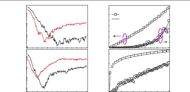
Figure 5. Characterization of thermal activation energy for hole and electron transport in C60@SWNT FETs. (a) Different transfer characteristics taken at VDS = 1.0 V for various temperatures from 250 K down to 4 K. Regions (I) and (III) are the on-states for hole and electron transport respectively. Region (II) is the subthreshold region (off-states) for p and n channels. (b) Thermal activation energy Ea as a function of gate voltage. (c) Energy band diagrams for different regions corresponding to (a).
The process of thermally assisted tunnelling transport is |
(III) is nearly independent of VGS, while it changes roughly |
||
strongly associated with the thermal activation energy Ea. |
linearly with VGS in region |
(II), i.e. VGS in the ranges of |
|
By using IDS(VGS, T ) exp(−Ea(VGS)/ kBT ) (where kB is |
−14 to −6 V and 14–21 V, respectively. In figure 5(c), we |
||
Boltzmann’s constant and T absolute temperature), Ea can be |
present energy band diagrams corresponding to each region |
||
extracted from the Arrhenius plot (similar to figure 4(b)) [30]. |
in figure 5(a). Thermal activation energy (Ea) is given by |
||
Figure 5(b) shows the variation of thermal activation energy |
the difference between the Fermi energy and the edge of the |
||
at various VGS values. For comparison, |
we present the |
nearest energy band (valence or conduction) of the SWNT. It |
|
corresponding temperature-dependent transfer characteristics |
can be seen that thermal activation energy Ea is a function |
||
for the same peapod device in figure 5(a). |
As denoted by |
of applied gate voltage VGS. |
For the on-states of a C60- |
red dash–dot lines, the ambipolar FET can operate in different |
peapod ambipolar FET, tunnelling transport is dominant for the |
||
states when we change VGS: the on-states for hole and electron |
injection of both electrons and holes due to the relatively lower |
||
transport (regions I and III in figure 5(a)) and the subthreshold |
Ea (figure 5(c) (I) and (III)). The slight variation of Ea, induced |
||
region of p and n type (region II in figure 5(a)). Interestingly, |
by applied VGS, has no distinct effect on the tunnelling process, |
||
we find that thermal activation energy Ea in regions (I) and |
and thus the on-state currents change little with temperature or |
||
2659