- •Preface
- •Imaging Microscopic Features
- •Measuring the Crystal Structure
- •References
- •Contents
- •1.4 Simulating the Effects of Elastic Scattering: Monte Carlo Calculations
- •What Are the Main Features of the Beam Electron Interaction Volume?
- •How Does the Interaction Volume Change with Composition?
- •How Does the Interaction Volume Change with Incident Beam Energy?
- •How Does the Interaction Volume Change with Specimen Tilt?
- •1.5 A Range Equation To Estimate the Size of the Interaction Volume
- •References
- •2: Backscattered Electrons
- •2.1 Origin
- •2.2.1 BSE Response to Specimen Composition (η vs. Atomic Number, Z)
- •SEM Image Contrast with BSE: “Atomic Number Contrast”
- •SEM Image Contrast: “BSE Topographic Contrast—Number Effects”
- •2.2.3 Angular Distribution of Backscattering
- •Beam Incident at an Acute Angle to the Specimen Surface (Specimen Tilt > 0°)
- •SEM Image Contrast: “BSE Topographic Contrast—Trajectory Effects”
- •2.2.4 Spatial Distribution of Backscattering
- •Depth Distribution of Backscattering
- •Radial Distribution of Backscattered Electrons
- •2.3 Summary
- •References
- •3: Secondary Electrons
- •3.1 Origin
- •3.2 Energy Distribution
- •3.3 Escape Depth of Secondary Electrons
- •3.8 Spatial Characteristics of Secondary Electrons
- •References
- •4: X-Rays
- •4.1 Overview
- •4.2 Characteristic X-Rays
- •4.2.1 Origin
- •4.2.2 Fluorescence Yield
- •4.2.3 X-Ray Families
- •4.2.4 X-Ray Nomenclature
- •4.2.6 Characteristic X-Ray Intensity
- •Isolated Atoms
- •X-Ray Production in Thin Foils
- •X-Ray Intensity Emitted from Thick, Solid Specimens
- •4.3 X-Ray Continuum (bremsstrahlung)
- •4.3.1 X-Ray Continuum Intensity
- •4.3.3 Range of X-ray Production
- •4.4 X-Ray Absorption
- •4.5 X-Ray Fluorescence
- •References
- •5.1 Electron Beam Parameters
- •5.2 Electron Optical Parameters
- •5.2.1 Beam Energy
- •Landing Energy
- •5.2.2 Beam Diameter
- •5.2.3 Beam Current
- •5.2.4 Beam Current Density
- •5.2.5 Beam Convergence Angle, α
- •5.2.6 Beam Solid Angle
- •5.2.7 Electron Optical Brightness, β
- •Brightness Equation
- •5.2.8 Focus
- •Astigmatism
- •5.3 SEM Imaging Modes
- •5.3.1 High Depth-of-Field Mode
- •5.3.2 High-Current Mode
- •5.3.3 Resolution Mode
- •5.3.4 Low-Voltage Mode
- •5.4 Electron Detectors
- •5.4.1 Important Properties of BSE and SE for Detector Design and Operation
- •Abundance
- •Angular Distribution
- •Kinetic Energy Response
- •5.4.2 Detector Characteristics
- •Angular Measures for Electron Detectors
- •Elevation (Take-Off) Angle, ψ, and Azimuthal Angle, ζ
- •Solid Angle, Ω
- •Energy Response
- •Bandwidth
- •5.4.3 Common Types of Electron Detectors
- •Backscattered Electrons
- •Passive Detectors
- •Scintillation Detectors
- •Semiconductor BSE Detectors
- •5.4.4 Secondary Electron Detectors
- •Everhart–Thornley Detector
- •Through-the-Lens (TTL) Electron Detectors
- •TTL SE Detector
- •TTL BSE Detector
- •Measuring the DQE: BSE Semiconductor Detector
- •References
- •6: Image Formation
- •6.1 Image Construction by Scanning Action
- •6.2 Magnification
- •6.3 Making Dimensional Measurements With the SEM: How Big Is That Feature?
- •Using a Calibrated Structure in ImageJ-Fiji
- •6.4 Image Defects
- •6.4.1 Projection Distortion (Foreshortening)
- •6.4.2 Image Defocusing (Blurring)
- •6.5 Making Measurements on Surfaces With Arbitrary Topography: Stereomicroscopy
- •6.5.1 Qualitative Stereomicroscopy
- •Fixed beam, Specimen Position Altered
- •Fixed Specimen, Beam Incidence Angle Changed
- •6.5.2 Quantitative Stereomicroscopy
- •Measuring a Simple Vertical Displacement
- •References
- •7: SEM Image Interpretation
- •7.1 Information in SEM Images
- •7.2.2 Calculating Atomic Number Contrast
- •Establishing a Robust Light-Optical Analogy
- •Getting It Wrong: Breaking the Light-Optical Analogy of the Everhart–Thornley (Positive Bias) Detector
- •Deconstructing the SEM/E–T Image of Topography
- •SUM Mode (A + B)
- •DIFFERENCE Mode (A−B)
- •References
- •References
- •9: Image Defects
- •9.1 Charging
- •9.1.1 What Is Specimen Charging?
- •9.1.3 Techniques to Control Charging Artifacts (High Vacuum Instruments)
- •Observing Uncoated Specimens
- •Coating an Insulating Specimen for Charge Dissipation
- •Choosing the Coating for Imaging Morphology
- •9.2 Radiation Damage
- •9.3 Contamination
- •References
- •10: High Resolution Imaging
- •10.2 Instrumentation Considerations
- •10.4.1 SE Range Effects Produce Bright Edges (Isolated Edges)
- •10.4.4 Too Much of a Good Thing: The Bright Edge Effect Hinders Locating the True Position of an Edge for Critical Dimension Metrology
- •10.5.1 Beam Energy Strategies
- •Low Beam Energy Strategy
- •High Beam Energy Strategy
- •Making More SE1: Apply a Thin High-δ Metal Coating
- •Making Fewer BSEs, SE2, and SE3 by Eliminating Bulk Scattering From the Substrate
- •10.6 Factors That Hinder Achieving High Resolution
- •10.6.2 Pathological Specimen Behavior
- •Contamination
- •Instabilities
- •References
- •11: Low Beam Energy SEM
- •11.3 Selecting the Beam Energy to Control the Spatial Sampling of Imaging Signals
- •11.3.1 Low Beam Energy for High Lateral Resolution SEM
- •11.3.2 Low Beam Energy for High Depth Resolution SEM
- •11.3.3 Extremely Low Beam Energy Imaging
- •References
- •12.1.1 Stable Electron Source Operation
- •12.1.2 Maintaining Beam Integrity
- •12.1.4 Minimizing Contamination
- •12.3.1 Control of Specimen Charging
- •12.5 VPSEM Image Resolution
- •References
- •13: ImageJ and Fiji
- •13.1 The ImageJ Universe
- •13.2 Fiji
- •13.3 Plugins
- •13.4 Where to Learn More
- •References
- •14: SEM Imaging Checklist
- •14.1.1 Conducting or Semiconducting Specimens
- •14.1.2 Insulating Specimens
- •14.2 Electron Signals Available
- •14.2.1 Beam Electron Range
- •14.2.2 Backscattered Electrons
- •14.2.3 Secondary Electrons
- •14.3 Selecting the Electron Detector
- •14.3.2 Backscattered Electron Detectors
- •14.3.3 “Through-the-Lens” Detectors
- •14.4 Selecting the Beam Energy for SEM Imaging
- •14.4.4 High Resolution SEM Imaging
- •Strategy 1
- •Strategy 2
- •14.5 Selecting the Beam Current
- •14.5.1 High Resolution Imaging
- •14.5.2 Low Contrast Features Require High Beam Current and/or Long Frame Time to Establish Visibility
- •14.6 Image Presentation
- •14.6.1 “Live” Display Adjustments
- •14.6.2 Post-Collection Processing
- •14.7 Image Interpretation
- •14.7.1 Observer’s Point of View
- •14.7.3 Contrast Encoding
- •14.8.1 VPSEM Advantages
- •14.8.2 VPSEM Disadvantages
- •15: SEM Case Studies
- •15.1 Case Study: How High Is That Feature Relative to Another?
- •15.2 Revealing Shallow Surface Relief
- •16.1.2 Minor Artifacts: The Si-Escape Peak
- •16.1.3 Minor Artifacts: Coincidence Peaks
- •16.1.4 Minor Artifacts: Si Absorption Edge and Si Internal Fluorescence Peak
- •16.2 “Best Practices” for Electron-Excited EDS Operation
- •16.2.1 Operation of the EDS System
- •Choosing the EDS Time Constant (Resolution and Throughput)
- •Choosing the Solid Angle of the EDS
- •Selecting a Beam Current for an Acceptable Level of System Dead-Time
- •16.3.1 Detector Geometry
- •16.3.2 Process Time
- •16.3.3 Optimal Working Distance
- •16.3.4 Detector Orientation
- •16.3.5 Count Rate Linearity
- •16.3.6 Energy Calibration Linearity
- •16.3.7 Other Items
- •16.3.8 Setting Up a Quality Control Program
- •Using the QC Tools Within DTSA-II
- •Creating a QC Project
- •Linearity of Output Count Rate with Live-Time Dose
- •Resolution and Peak Position Stability with Count Rate
- •Solid Angle for Low X-ray Flux
- •Maximizing Throughput at Moderate Resolution
- •References
- •17: DTSA-II EDS Software
- •17.1 Getting Started With NIST DTSA-II
- •17.1.1 Motivation
- •17.1.2 Platform
- •17.1.3 Overview
- •17.1.4 Design
- •Simulation
- •Quantification
- •Experiment Design
- •Modeled Detectors (. Fig. 17.1)
- •Window Type (. Fig. 17.2)
- •The Optimal Working Distance (. Figs. 17.3 and 17.4)
- •Elevation Angle
- •Sample-to-Detector Distance
- •Detector Area
- •Crystal Thickness
- •Number of Channels, Energy Scale, and Zero Offset
- •Resolution at Mn Kα (Approximate)
- •Azimuthal Angle
- •Gold Layer, Aluminum Layer, Nickel Layer
- •Dead Layer
- •Zero Strobe Discriminator (. Figs. 17.7 and 17.8)
- •Material Editor Dialog (. Figs. 17.9, 17.10, 17.11, 17.12, 17.13, and 17.14)
- •17.2.1 Introduction
- •17.2.2 Monte Carlo Simulation
- •17.2.4 Optional Tables
- •References
- •18: Qualitative Elemental Analysis by Energy Dispersive X-Ray Spectrometry
- •18.1 Quality Assurance Issues for Qualitative Analysis: EDS Calibration
- •18.2 Principles of Qualitative EDS Analysis
- •Exciting Characteristic X-Rays
- •Fluorescence Yield
- •X-ray Absorption
- •Si Escape Peak
- •Coincidence Peaks
- •18.3 Performing Manual Qualitative Analysis
- •Beam Energy
- •Choosing the EDS Resolution (Detector Time Constant)
- •Obtaining Adequate Counts
- •18.4.1 Employ the Available Software Tools
- •18.4.3 Lower Photon Energy Region
- •18.4.5 Checking Your Work
- •18.5 A Worked Example of Manual Peak Identification
- •References
- •19.1 What Is a k-ratio?
- •19.3 Sets of k-ratios
- •19.5 The Analytical Total
- •19.6 Normalization
- •19.7.1 Oxygen by Assumed Stoichiometry
- •19.7.3 Element by Difference
- •19.8 Ways of Reporting Composition
- •19.8.1 Mass Fraction
- •19.8.2 Atomic Fraction
- •19.8.3 Stoichiometry
- •19.8.4 Oxide Fractions
- •Example Calculations
- •19.9 The Accuracy of Quantitative Electron-Excited X-ray Microanalysis
- •19.9.1 Standards-Based k-ratio Protocol
- •19.9.2 “Standardless Analysis”
- •19.10 Appendix
- •19.10.1 The Need for Matrix Corrections To Achieve Quantitative Analysis
- •19.10.2 The Physical Origin of Matrix Effects
- •19.10.3 ZAF Factors in Microanalysis
- •X-ray Generation With Depth, φ(ρz)
- •X-ray Absorption Effect, A
- •X-ray Fluorescence, F
- •References
- •20.2 Instrumentation Requirements
- •20.2.1 Choosing the EDS Parameters
- •EDS Spectrum Channel Energy Width and Spectrum Energy Span
- •EDS Time Constant (Resolution and Throughput)
- •EDS Calibration
- •EDS Solid Angle
- •20.2.2 Choosing the Beam Energy, E0
- •20.2.3 Measuring the Beam Current
- •20.2.4 Choosing the Beam Current
- •Optimizing Analysis Strategy
- •20.3.4 Ba-Ti Interference in BaTiSi3O9
- •20.4 The Need for an Iterative Qualitative and Quantitative Analysis Strategy
- •20.4.2 Analysis of a Stainless Steel
- •20.5 Is the Specimen Homogeneous?
- •20.6 Beam-Sensitive Specimens
- •20.6.1 Alkali Element Migration
- •20.6.2 Materials Subject to Mass Loss During Electron Bombardment—the Marshall-Hall Method
- •Thin Section Analysis
- •Bulk Biological and Organic Specimens
- •References
- •21: Trace Analysis by SEM/EDS
- •21.1 Limits of Detection for SEM/EDS Microanalysis
- •21.2.1 Estimating CDL from a Trace or Minor Constituent from Measuring a Known Standard
- •21.2.2 Estimating CDL After Determination of a Minor or Trace Constituent with Severe Peak Interference from a Major Constituent
- •21.3 Measurements of Trace Constituents by Electron-Excited Energy Dispersive X-ray Spectrometry
- •The Inevitable Physics of Remote Excitation Within the Specimen: Secondary Fluorescence Beyond the Electron Interaction Volume
- •Simulation of Long-Range Secondary X-ray Fluorescence
- •NIST DTSA II Simulation: Vertical Interface Between Two Regions of Different Composition in a Flat Bulk Target
- •NIST DTSA II Simulation: Cubic Particle Embedded in a Bulk Matrix
- •21.5 Summary
- •References
- •22.1.2 Low Beam Energy Analysis Range
- •22.2 Advantage of Low Beam Energy X-Ray Microanalysis
- •22.2.1 Improved Spatial Resolution
- •22.3 Challenges and Limitations of Low Beam Energy X-Ray Microanalysis
- •22.3.1 Reduced Access to Elements
- •22.3.3 At Low Beam Energy, Almost Everything Is Found To Be Layered
- •Analysis of Surface Contamination
- •References
- •23: Analysis of Specimens with Special Geometry: Irregular Bulk Objects and Particles
- •23.2.1 No Chemical Etching
- •23.3 Consequences of Attempting Analysis of Bulk Materials With Rough Surfaces
- •23.4.1 The Raw Analytical Total
- •23.4.2 The Shape of the EDS Spectrum
- •23.5 Best Practices for Analysis of Rough Bulk Samples
- •23.6 Particle Analysis
- •Particle Sample Preparation: Bulk Substrate
- •The Importance of Beam Placement
- •Overscanning
- •“Particle Mass Effect”
- •“Particle Absorption Effect”
- •The Analytical Total Reveals the Impact of Particle Effects
- •Does Overscanning Help?
- •23.6.6 Peak-to-Background (P/B) Method
- •Specimen Geometry Severely Affects the k-ratio, but Not the P/B
- •Using the P/B Correspondence
- •23.7 Summary
- •References
- •24: Compositional Mapping
- •24.2 X-Ray Spectrum Imaging
- •24.2.1 Utilizing XSI Datacubes
- •24.2.2 Derived Spectra
- •SUM Spectrum
- •MAXIMUM PIXEL Spectrum
- •24.3 Quantitative Compositional Mapping
- •24.4 Strategy for XSI Elemental Mapping Data Collection
- •24.4.1 Choosing the EDS Dead-Time
- •24.4.2 Choosing the Pixel Density
- •24.4.3 Choosing the Pixel Dwell Time
- •“Flash Mapping”
- •High Count Mapping
- •References
- •25.1 Gas Scattering Effects in the VPSEM
- •25.1.1 Why Doesn’t the EDS Collimator Exclude the Remote Skirt X-Rays?
- •25.2 What Can Be Done To Minimize gas Scattering in VPSEM?
- •25.2.2 Favorable Sample Characteristics
- •Particle Analysis
- •25.2.3 Unfavorable Sample Characteristics
- •References
- •26.1 Instrumentation
- •26.1.2 EDS Detector
- •26.1.3 Probe Current Measurement Device
- •Direct Measurement: Using a Faraday Cup and Picoammeter
- •A Faraday Cup
- •Electrically Isolated Stage
- •Indirect Measurement: Using a Calibration Spectrum
- •26.1.4 Conductive Coating
- •26.2 Sample Preparation
- •26.2.1 Standard Materials
- •26.2.2 Peak Reference Materials
- •26.3 Initial Set-Up
- •26.3.1 Calibrating the EDS Detector
- •Selecting a Pulse Process Time Constant
- •Energy Calibration
- •Quality Control
- •Sample Orientation
- •Detector Position
- •Probe Current
- •26.4 Collecting Data
- •26.4.1 Exploratory Spectrum
- •26.4.2 Experiment Optimization
- •26.4.3 Selecting Standards
- •26.4.4 Reference Spectra
- •26.4.5 Collecting Standards
- •26.4.6 Collecting Peak-Fitting References
- •26.5 Data Analysis
- •26.5.2 Quantification
- •26.6 Quality Check
- •Reference
- •27.2 Case Study: Aluminum Wire Failures in Residential Wiring
- •References
- •28: Cathodoluminescence
- •28.1 Origin
- •28.2 Measuring Cathodoluminescence
- •28.3 Applications of CL
- •28.3.1 Geology
- •Carbonado Diamond
- •Ancient Impact Zircons
- •28.3.2 Materials Science
- •Semiconductors
- •Lead-Acid Battery Plate Reactions
- •28.3.3 Organic Compounds
- •References
- •29.1.1 Single Crystals
- •29.1.2 Polycrystalline Materials
- •29.1.3 Conditions for Detecting Electron Channeling Contrast
- •Specimen Preparation
- •Instrument Conditions
- •29.2.1 Origin of EBSD Patterns
- •29.2.2 Cameras for EBSD Pattern Detection
- •29.2.3 EBSD Spatial Resolution
- •29.2.5 Steps in Typical EBSD Measurements
- •Sample Preparation for EBSD
- •Align Sample in the SEM
- •Check for EBSD Patterns
- •Adjust SEM and Select EBSD Map Parameters
- •Run the Automated Map
- •29.2.6 Display of the Acquired Data
- •29.2.7 Other Map Components
- •29.2.10 Application Example
- •Application of EBSD To Understand Meteorite Formation
- •29.2.11 Summary
- •Specimen Considerations
- •EBSD Detector
- •Selection of Candidate Crystallographic Phases
- •Microscope Operating Conditions and Pattern Optimization
- •Selection of EBSD Acquisition Parameters
- •Collect the Orientation Map
- •References
- •30.1 Introduction
- •30.2 Ion–Solid Interactions
- •30.3 Focused Ion Beam Systems
- •30.5 Preparation of Samples for SEM
- •30.5.1 Cross-Section Preparation
- •30.5.2 FIB Sample Preparation for 3D Techniques and Imaging
- •30.6 Summary
- •References
- •31: Ion Beam Microscopy
- •31.1 What Is So Useful About Ions?
- •31.2 Generating Ion Beams
- •31.3 Signal Generation in the HIM
- •31.5 Patterning with Ion Beams
- •31.7 Chemical Microanalysis with Ion Beams
- •References
- •Appendix
- •A Database of Electron–Solid Interactions
- •Introduction
- •Backscattered Electrons
- •Secondary Yields
- •Stopping Powers
- •X-ray Ionization Cross Sections
- •Conclusions
- •References
- •Index
- •Reference List
- •Index
\16 Chapter 2 · Backscattered Electrons
2.1\ Origin
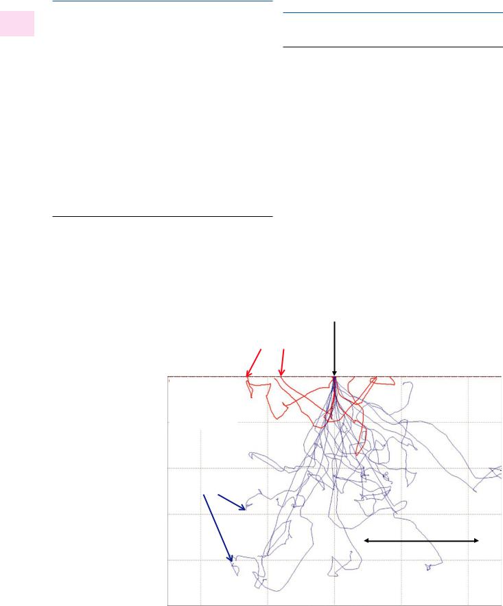
Close inspection of the trajectories in the Monte Carlo simu- 2 lation of a flat, bulk target of copper at 0° tilt shown in
. Fig. 2.1 reveals that a significant fraction of the incident beam electrons undergo sufficient scattering events to completely reverse their initial direction of travel into the specimen, causing these electrons to return to the entrance surface and exit the specimen. These beam electrons that escape from the specimen are referred to as “backscattered electrons” (BSE) and constitute an important SEM imaging signal rich in information on specimen characteristics. The BSE signal can convey information on the specimen composition, topography, mass thickness, and crystallography. This module describes the properties of backscattered electrons and how those properties are modified by specimen characteristics to produce useful information in SEM images.
2.1.1\ The Numerical Measure of
Backscattered Electrons
Backscattered electrons are quantified with the “backscattered electron coefficient,” η, defined as
η = NBSE / NB \ |
(2.1) |
where NB is the number of beam electrons that enter the specimen and NBSE is the number of those electrons that subsequently emerge as backscattered electrons.
2.2\ Critical Properties of Backscattered
Electrons
2.2.1\ BSE Response to Specimen Composition (η vs. Atomic Number, Z)
Use the CASINO Monte Carlo simulation software, which reports η in the output, to examine the dependence of electron backscattering on the atomic number of the specimen.
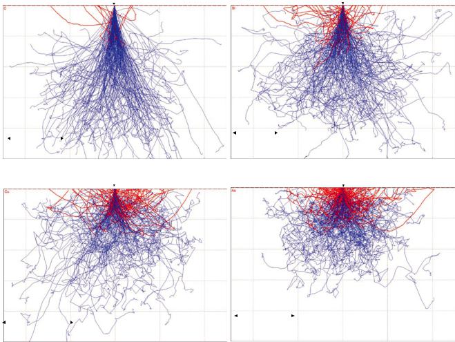
Simulate at least 10,000 trajectories at an incident energy of E0 = 20 keV and a surface tilt of 0° (i.e., the beam is perpendicular to the surface). Note that statistical variations will be observed in the calculation of η due to the different selections of the random numbers used in each simulation. Repetitions of this calculation will give a distribution of results, with a precision p = (η N)1/2/η N, so that for N = 10,000 trajectories and η ~ 0.15 (Si), p is expected to be 2.5 %. . Figure 2.2 shows the simulation of 500 trajectories in carbon, silicon, copper, and gold with an incident energy of E0 = 20 keV and a surface tilt of 0°, showing qualitatively the increase in the number of backscattered electrons with atomic number.
Detailed experimental measurements of the backscattered electron coefficient as a function of the atomic number, Z, in highly polished, flat pure element targets confirm a generally monotonic increase in η with increasing Z, as shown in
. Fig. 2.3a, where the classic measurements made by Heinrich (1966) at a beam energy of 20 keV are plotted. The slope of η vs. Z is highest for low atomic number targets up to approximately Z =14 (Si). As Z continues to increase into the range of
. Fig. 2.1 Monte Carlo simulation of a flat, bulk target of
copper at 0° tilt. Red trajectories BSE lead to backscattering events
0.0 nm
Cu
E0 = 20 keV 0° Tilt
200.0 nm
Absorbed Electrons
(lost all energy and are 400.0 nm absorbed within specimen)
600.0 nm
500 nm
800.0 nm
-582.5 nm |
-291.3 nm |
-0.0 nm |
291.3 nm |
582.5 nm |
2.2 · Critical Properties of Backscattered Electrons |
|
|
|
|
|
|
|
|
|
|
17 |
|
|
2 |
||||||||
|
|
|
|
|
|
|
|
|
|
|
|
|
|
|||||||||
a |
|
|
|
|
|
|
|
b |
|
|
|
|
|
|
|
|
|
|||||
|
|
|
|
|
|
|
|
|
|
|
|
|
|
|
|
|||||||
|
|
|
|
|
|
|
|
|
0.0 nm |
|
|
|
|
|
|
|
|
|
|
|
|
0.0 nm |
|
|
|
|
|
|
|
|
|
|
|
|
|
|
|
|
|
|
|
|
|
||
|
|
|
|
|
|
|
|
|
624.9 nm |
|
|
|
|
|
|
|
|
|
|
|
|
755.3 nm |
|
|
|
|
|
|
|
|
|
1249.7 nm |
|
|
|
|
|
|
|
|
|
|
|
1510.6 nm |
|
|
|
|
|
|
|
|
|
|
1874.6 nm |
|
|
|
|
|
|
|
|
|
|
|
2265.9 nm |
|
|
C |
|
|
|
|
|
|
|
Si |
|
|
|
|
|
|
|
|
|
||||
|
E0 = 20 keV |
|
|
|
|
|
|
2499.4 nm |
E0 = 20 keV |
|
|
|
|
|
|
|
3021.3 nm |
|||||
|
|
|
|
|
|
|
|
|
|
|
|
1 µm |
|
|
|
|
|
|
|
|
|
|
|
|
1 µm |
|
|
|
|
|
|
|
|
|
|
|
|
|
|
|
|
|
|
|
|
|
|
-1820.0 nm |
-910.0 nm |
-0.0 nm |
910.0 nm |
1820.0 nm |
|
|
-2200.0 nm |
-1100.0 nm |
-0.0 nm |
1100.0 nm |
2200.0 nm |
|||||||||
|
c |
|
|
|
|
|
|
|
d |
|
|
|
|
|
|
|
|
|
||||
|
|
|
|
|
|
|
|
|
|
|
|
|
|
|
|
|
||||||
|
|
|
|
|
|
|
|
|
0.0 nm |
|
|
|
|
|
|
|
|
|
|
|
|
0.0 nm |
|
|
|
|
|
|
|
|
|
|
|
|
|
|
|
|
|
|
|
|
|
||
|
|
|
|
|
|
|
|
|
233.5 nm |
|
|
|
|
|
|
|
|
|
|
|
|
137.3 nm |
|
|
|
|
|
|
|
|
|
466.9 nm |
|
|
|
|
|
|
|
|
|
|
|
|
274.7 nm |
|
|
|
|
|
|
|
|
|
700.4 nm |
|
|
|
|
|
|
|
|
|
|
|
|
412.0 nm |
|
|
|
|
|
|
|
|
|
|
|
|
Au |
|
|
|
|
|
|
|
|
|
|
|
Cu |
|
|
|
|
|
|
933.8 nm |
|
|
E0 = 20 keV |
|
|
|
|
|
|
|
|
549.3 nm |
||
|
E0 = 20 keV |
|
|
|
|
|
|
|
|
|
|
|
|
|
|
|
|
|
|
|||
|
|
|
|
|
|
|
|
|
|
250 nm |
|
|
|
|
|
|
|
|
|
|||
|
|
500 nm |
|
|
|
|
|
|
|
|
|
|
|
|
|
|
|
|
|
|
||
|
|
|
|
|
|
|
|
|
|
|
|
|
|
|
|
|
|
|
|
|
|
|
|
|
-680.0 nm |
-340.0 nm |
-0.0 nm |
340.0 nm |
680.0 nm |
|
|
-400.0 nm |
-200.0 nm |
-0.0 nm |
200.0 nm |
400.0 nm |
. Fig. 2.2 a Monte Carlo simulation of 500 trajectories in carbon with an incident energy of E0 = 20 keV and a surface tilt of 0° (CASINO Monte Carlo simulation). b Monte Carlo simulation of 500 trajectories in silicon with an incident energy of E0 = 20 keV and a surface tilt of 0°.
the transition elements, e.g., Z=26 (Fe), the slope progressively decreases until at very high Z, e.g., the region around Z=79 (Au), the slope becomes so shallow that there is very little change in η between adjacent elements. Plotted in addition to the experimental measurements in . Fig. 2.3a is a mathematical fit to the 20 keV data developed by Reuter (1972):
η = − 0.0254 + 0.016 Z −1.86 ×10⁻⁴ Z2 +8.3×10⁻⁷ Z3 |
\ |
(2.2) |
|
|
This fit provides a convenient estimate of η for those elements for which direct measurements do not exist.
Experimental measurements (Heinrich 1966) have shown that the backscattered electron coefficient of a mixture of atoms that is homogeneous on the atomic scale, such as a stoichiometric compound, a glass, or certain metallic alloys, can be accurately predicted from the mass concentrations of the elemental constituents and the values of η for those pure elements:
c Monte Carlo simulation of 500 trajectories in copper with an incident energy of E0 = 20 keV and a surface tilt of 0°. d Monte Carlo simulation of 500 trajectories in gold with an incident energy of E0 = 20 keV and a surface tilt of 0°. Red trajectories = backscattering
ηmixture =ΣηiCi \ |
(2.3) |
where C is the mass (weight) fraction and i is an index that denotes all of the elements involved.
When measurements of η vs. Z are made at different beam energies, combining the experimental measurements of Heinrich and of Bishop in . Fig. 2.3b, little dependence on the beam energy is found from 5 to 49 keV, with all of the measurements clustering relatively closely to the curve for the 20 keV data shown in . Fig. 2.3a. This result is perhaps surprising in view of the strong dependence of the dimensions of the interaction volume on the incident beam energy. The weak dependence of η upon E0 despite the strong dependence of the beam penetration upon E0 can be understood as a near balance between the increased energy available at higher E0, the lower rate of loss, dE/ds, with higher E0, and the increased penetration. Thus, although a beam electron may penetrate more deeply at high E0, it started with more
18\ Chapter 2 · Backscattered Electrons
. Fig. 2.3 a Electron backscatter coefficient as a function of atomic number for pure elements (Data of Heinrich 1966; fit of Reuter 1972).
2 b Electron backscatter coefficient as a function of atomic number for pure elements for incident beam energies of 5 keV (data of Bishop 1966); 10 keV to 49 keV (Data of Heinrich 1966); Reuter’s fit to Heinrich’s 20 keV data, (1972))
a
|
0.6 |
|
coefficient |
0.5 |
|
0.4 |
||
|
||
Backscatter |
0.3 |
|
0.2 |
||
|
0.1 |
|
|
0.0 |
0
b
|
0.6 |
|
|
coefficient |
0.5 |
|
|
0.4 |
|
|
|
|
|
|
|
Backscatter |
0.3 |
|
|
0.2 |
|
|
|
|
|
||
|
|
||
|
0.1 |
|
|
|
|
|
|
|
|
|
|
|
|
|
|
|
|
|
|
|
|
|
|
|
0.0 |
|
|
|
|
|
|
|
|
|
0
Electron backscatter vs. atomic number (E0 = 20 keV)
Reuter Fit
Heinrich 20 keV data
20 40 60 80 100 Atomic number
Electron backscattering vs. atomic number
Heinrich 10 keV
Heinrich 20 keV
Heinrich 30 keV
Heinrich 40 keV
Heinrich 49 keV
Bishop 5 keV
Reuter fit 20 keV
20 |
40 |
60 |
80 |
100 |
|
Atomic number |
|
|
energy and lost that energy at a lower initial rate than an electron at a lower incidence energy. Thus, a higher incidence energy electron, despite penetrating deeper in the specimen, retains more energy and can continue to scatter and progress through the target to escape.
SEM Image Contrast with BSE: “Atomic Number Contrast”
Whenever a signal that can be measured in the SEM, such as backscattered electrons, follows a predictable response to a specimen property of interest, such as composition, the physical basis for a “contrast mechanism” is established. Contrast, Ctr, is defined as
2.2 · Critical Properties of Backscattered Electrons
Ctr = (S2 − S1 ) / S2 with S2 > S1 |
\ |
(2.4) |
|
|
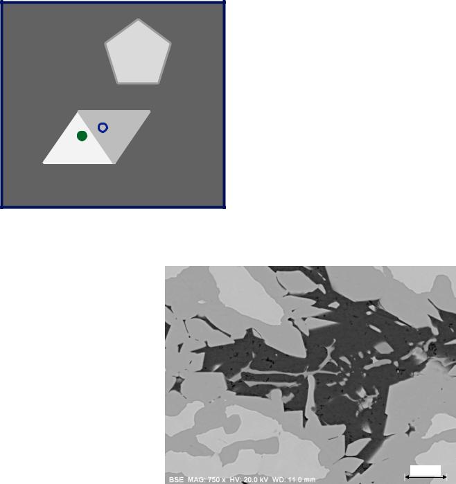
where S is the signal measured at any two locations of interest in the image field. As shown in . Fig. 2.4, examples include the contrast between an object P1 and the general background P2 or between two objects that share an interface, P3 and P4. By this definition, contrast can range numerically from 0 to 1.
• P2 • P1
P4
P3
. Fig. 2.4 Illustration of some possible contrast situations of interest, e.g., an object P1 and the general background P2 or between two objects that share an interface, P3 and P4
. Fig. 2.5 Backscattered electron atomic number contrast for a polished flat surface of Raney nickel (nickel-aluminum) alloy. Numbered locations identify phases with distinctly different compositions
19 |
|
2 |
|
|
|
The monotonic behavior of η vs. Z establishes the physical basis for “atomic number contrast” (also known as “Z-contrast” and “compositional contrast”). When an SEM BSE image is acquired from a flat specimen (i.e., no topography is present, at least on a scale no greater than about 5 % of the Kanaya–Okayama range for the particular material composition and incident beam energy), then local differences in composition can be observed as differences in the BSE intensity, which can be used to construct a meaningful gray-scale SEM image. The compositionally-different objects must have dimensions that are at least as large as the Kanaya-Okayama range for each distinct material so that a BSE signal characteristic of the particular composition can be measured over at least the center portion of the object. The BSE signal at beam locations on the edge of the object may be affected by penetration into the neighboring material(s).
From the definition of contrast, Ctr, atomic number contrast can be predicted between two materials with backscatter coefficients η1 and η2 when the measured signal S is proportional to η:
Ctr = (η2 −η1 ) /η2 with η2 > η1 \ |
(2.5) |
An example of atomic number contrast from a polished cross section of an aluminum-nickel alloy (Raney nickel) is shown in . Fig. 2.5. At least four distinct gray levels are observed, which correspond to three different Al/Ni phases with different Al-Ni compositions (labeled “1,” “3,” and “4” in . Fig. 2.5) and a fourth phase that consists of Al-Fe-Ni (labelled “2”), with the phase containing the highest nickel concentration appearing brightest in the BSE image.
3 2 1
4
10 µm
\20 Chapter 2 · Backscattered Electrons
|
2.2.2\ |
BSE Response to Specimen Inclination |
||
|
|
|
(η vs. Surface Tilt, θ) |
|
2 |
Model the effect of the angle of inclination of the specimen sur- |
|||
|
face to the incident beam with the Monte Carlo simulation. |
|||
|
||||
|
Select a particular element and incident beam energy, e.g., cop- |
|||
|
per and E0 = 20 keV, and vary the angle of incidence. Calculate |
|||
|
|
at least 10,000 trajectories to obtain adequate simulation |
||
|
|
precision. |
||
|
|
. Figure 2.6 shows simulations for aluminum with an |
||
|
|
incident beam energy of 15 keV at various inclinations calcu- |
||
|
|
lated with 200 trajectories, which qualitatively reveals the |
||
|
|
increase in backscattering in a forward direction (i.e., con- |
||
|
|
tinuing in the general direction of the incident beam) with |
||
|
|
increasing tilt angle. A more extensive series of simulations |
||
|
|
for aluminum at E0 = 15 keV with 25,000 trajectories cover- |
||
|
ing a greater range of specimen tilts is presented in . Table 2.1, |
|||
|
where the backscatter coefficient shows a strong dependence |
|||
|
on the surface inclination. |
|||
|
|
a |
|
b |
. Table 2.1 Backscatter vs. tilt angle for aluminum at E0 = 15 keV (25,000 trajectories calculated with the CASINO Monte Carlo simulation)
Tilt (degrees) |
η |
|
|
0 |
0.129 |
|
|
15 |
0.138 |
30 |
0.169 |
45 |
0.242 |
60 |
0.367 |
75 |
0.531 |
80 |
0.612 |
85 |
0.706 |
88 |
0.796 |
89 |
0.826 |
AI |
|
|
|
0.0 nm |
AI |
|
|
|
0.0 nm |
||
|
|
|
|
|
|
487.5 nm |
|
|
|
|
330.0 nm |
|
|
|
|
|
|
975.0 nm |
|
|
|
|
660.0 nm |
Al |
|
|
|
1462.6 nm |
Al |
|
|
|
990.0 nm |
||
|
|
|
|
|
|
|
|
||||
E0 = 15 keV |
|
|
|
|
E0= 15 keV |
|
|
|
|
||
0∞ tilt |
|
|
|
1950.1 nm |
45∞ tilt |
|
|
|
|
||
|
|
|
|
|
|
500 nm |
|
|
|
1320.0 nm |
|
|
500 nm |
|
|
|
|
|
|
|
|
||
|
|
|
|
|
|
|
|
|
|
||
-1420.2 nm |
-710.0 nm |
-0.0 nm |
710.0 nm |
1420.0 nm |
-961.2 nm |
-480.6 nm |
-0.0 nm |
480.6 nm |
961.2 nm |
||
c |
|
|
|
|
d |
|
|
|
|
||
AI |
|
|
|
0.0 nm |
AI |
|
|
|
0.0 nm |
||
|
|
|
|
|
|
420.0 nm |
|
|
|
|
240.0 nm |
|
|
|
|
|
|
840.0 nm |
|
|
|
|
480.0 nm |
|
|
|
|
|
|
1260.0 nm |
Al |
|
|
|
720.0 nm |
Al |
|
|
|
|
|
|
|
|
|||
E0 = 15 keV |
|
|
|
|
E0 = 15 keV |
|
|
|
|||
60∞ tilt |
|
|
|
1680.0 nm |
75∞ tilt |
|
|
|
960.0 nm |
||
|
|
|
|
|
|
|
|
|
|
||
|
500 nm |
|
|
|
|
500 nm |
|
|
|
|
|
-1223.3 nm |
-611.7 nm |
-0.0 nm |
611.7 nm |
1223.3 nm |
-699.0 nm |
-349.5 nm |
-0.0 nm |
349.5 nm |
699.0 nm |
. Fig. 2.6 a Monte Carlo simulation for aluminum at E0 = 15 keV for a tilt angle of 0°. b Monte Carlo simulation for aluminum at E0 = 15 keV for a tilt angle of 45°. c Monte Carlo simulation for aluminum at
E0 = 15 keV for a tilt angle of 60°. d Monte Carlo simulation for aluminum at E0 = 15 keV for a tilt angle of 75°