

- •Preface
- •Imaging Microscopic Features
- •Measuring the Crystal Structure
- •References
- •Contents
- •1.4 Simulating the Effects of Elastic Scattering: Monte Carlo Calculations
- •What Are the Main Features of the Beam Electron Interaction Volume?
- •How Does the Interaction Volume Change with Composition?
- •How Does the Interaction Volume Change with Incident Beam Energy?
- •How Does the Interaction Volume Change with Specimen Tilt?
- •1.5 A Range Equation To Estimate the Size of the Interaction Volume
- •References
- •2: Backscattered Electrons
- •2.1 Origin
- •2.2.1 BSE Response to Specimen Composition (η vs. Atomic Number, Z)
- •SEM Image Contrast with BSE: “Atomic Number Contrast”
- •SEM Image Contrast: “BSE Topographic Contrast—Number Effects”
- •2.2.3 Angular Distribution of Backscattering
- •Beam Incident at an Acute Angle to the Specimen Surface (Specimen Tilt > 0°)
- •SEM Image Contrast: “BSE Topographic Contrast—Trajectory Effects”
- •2.2.4 Spatial Distribution of Backscattering
- •Depth Distribution of Backscattering
- •Radial Distribution of Backscattered Electrons
- •2.3 Summary
- •References
- •3: Secondary Electrons
- •3.1 Origin
- •3.2 Energy Distribution
- •3.3 Escape Depth of Secondary Electrons
- •3.8 Spatial Characteristics of Secondary Electrons
- •References
- •4: X-Rays
- •4.1 Overview
- •4.2 Characteristic X-Rays
- •4.2.1 Origin
- •4.2.2 Fluorescence Yield
- •4.2.3 X-Ray Families
- •4.2.4 X-Ray Nomenclature
- •4.2.6 Characteristic X-Ray Intensity
- •Isolated Atoms
- •X-Ray Production in Thin Foils
- •X-Ray Intensity Emitted from Thick, Solid Specimens
- •4.3 X-Ray Continuum (bremsstrahlung)
- •4.3.1 X-Ray Continuum Intensity
- •4.3.3 Range of X-ray Production
- •4.4 X-Ray Absorption
- •4.5 X-Ray Fluorescence
- •References
- •5.1 Electron Beam Parameters
- •5.2 Electron Optical Parameters
- •5.2.1 Beam Energy
- •Landing Energy
- •5.2.2 Beam Diameter
- •5.2.3 Beam Current
- •5.2.4 Beam Current Density
- •5.2.5 Beam Convergence Angle, α
- •5.2.6 Beam Solid Angle
- •5.2.7 Electron Optical Brightness, β
- •Brightness Equation
- •5.2.8 Focus
- •Astigmatism
- •5.3 SEM Imaging Modes
- •5.3.1 High Depth-of-Field Mode
- •5.3.2 High-Current Mode
- •5.3.3 Resolution Mode
- •5.3.4 Low-Voltage Mode
- •5.4 Electron Detectors
- •5.4.1 Important Properties of BSE and SE for Detector Design and Operation
- •Abundance
- •Angular Distribution
- •Kinetic Energy Response
- •5.4.2 Detector Characteristics
- •Angular Measures for Electron Detectors
- •Elevation (Take-Off) Angle, ψ, and Azimuthal Angle, ζ
- •Solid Angle, Ω
- •Energy Response
- •Bandwidth
- •5.4.3 Common Types of Electron Detectors
- •Backscattered Electrons
- •Passive Detectors
- •Scintillation Detectors
- •Semiconductor BSE Detectors
- •5.4.4 Secondary Electron Detectors
- •Everhart–Thornley Detector
- •Through-the-Lens (TTL) Electron Detectors
- •TTL SE Detector
- •TTL BSE Detector
- •Measuring the DQE: BSE Semiconductor Detector
- •References
- •6: Image Formation
- •6.1 Image Construction by Scanning Action
- •6.2 Magnification
- •6.3 Making Dimensional Measurements With the SEM: How Big Is That Feature?
- •Using a Calibrated Structure in ImageJ-Fiji
- •6.4 Image Defects
- •6.4.1 Projection Distortion (Foreshortening)
- •6.4.2 Image Defocusing (Blurring)
- •6.5 Making Measurements on Surfaces With Arbitrary Topography: Stereomicroscopy
- •6.5.1 Qualitative Stereomicroscopy
- •Fixed beam, Specimen Position Altered
- •Fixed Specimen, Beam Incidence Angle Changed
- •6.5.2 Quantitative Stereomicroscopy
- •Measuring a Simple Vertical Displacement
- •References
- •7: SEM Image Interpretation
- •7.1 Information in SEM Images
- •7.2.2 Calculating Atomic Number Contrast
- •Establishing a Robust Light-Optical Analogy
- •Getting It Wrong: Breaking the Light-Optical Analogy of the Everhart–Thornley (Positive Bias) Detector
- •Deconstructing the SEM/E–T Image of Topography
- •SUM Mode (A + B)
- •DIFFERENCE Mode (A−B)
- •References
- •References
- •9: Image Defects
- •9.1 Charging
- •9.1.1 What Is Specimen Charging?
- •9.1.3 Techniques to Control Charging Artifacts (High Vacuum Instruments)
- •Observing Uncoated Specimens
- •Coating an Insulating Specimen for Charge Dissipation
- •Choosing the Coating for Imaging Morphology
- •9.2 Radiation Damage
- •9.3 Contamination
- •References
- •10: High Resolution Imaging
- •10.2 Instrumentation Considerations
- •10.4.1 SE Range Effects Produce Bright Edges (Isolated Edges)
- •10.4.4 Too Much of a Good Thing: The Bright Edge Effect Hinders Locating the True Position of an Edge for Critical Dimension Metrology
- •10.5.1 Beam Energy Strategies
- •Low Beam Energy Strategy
- •High Beam Energy Strategy
- •Making More SE1: Apply a Thin High-δ Metal Coating
- •Making Fewer BSEs, SE2, and SE3 by Eliminating Bulk Scattering From the Substrate
- •10.6 Factors That Hinder Achieving High Resolution
- •10.6.2 Pathological Specimen Behavior
- •Contamination
- •Instabilities
- •References
- •11: Low Beam Energy SEM
- •11.3 Selecting the Beam Energy to Control the Spatial Sampling of Imaging Signals
- •11.3.1 Low Beam Energy for High Lateral Resolution SEM
- •11.3.2 Low Beam Energy for High Depth Resolution SEM
- •11.3.3 Extremely Low Beam Energy Imaging
- •References
- •12.1.1 Stable Electron Source Operation
- •12.1.2 Maintaining Beam Integrity
- •12.1.4 Minimizing Contamination
- •12.3.1 Control of Specimen Charging
- •12.5 VPSEM Image Resolution
- •References
- •13: ImageJ and Fiji
- •13.1 The ImageJ Universe
- •13.2 Fiji
- •13.3 Plugins
- •13.4 Where to Learn More
- •References
- •14: SEM Imaging Checklist
- •14.1.1 Conducting or Semiconducting Specimens
- •14.1.2 Insulating Specimens
- •14.2 Electron Signals Available
- •14.2.1 Beam Electron Range
- •14.2.2 Backscattered Electrons
- •14.2.3 Secondary Electrons
- •14.3 Selecting the Electron Detector
- •14.3.2 Backscattered Electron Detectors
- •14.3.3 “Through-the-Lens” Detectors
- •14.4 Selecting the Beam Energy for SEM Imaging
- •14.4.4 High Resolution SEM Imaging
- •Strategy 1
- •Strategy 2
- •14.5 Selecting the Beam Current
- •14.5.1 High Resolution Imaging
- •14.5.2 Low Contrast Features Require High Beam Current and/or Long Frame Time to Establish Visibility
- •14.6 Image Presentation
- •14.6.1 “Live” Display Adjustments
- •14.6.2 Post-Collection Processing
- •14.7 Image Interpretation
- •14.7.1 Observer’s Point of View
- •14.7.3 Contrast Encoding
- •14.8.1 VPSEM Advantages
- •14.8.2 VPSEM Disadvantages
- •15: SEM Case Studies
- •15.1 Case Study: How High Is That Feature Relative to Another?
- •15.2 Revealing Shallow Surface Relief
- •16.1.2 Minor Artifacts: The Si-Escape Peak
- •16.1.3 Minor Artifacts: Coincidence Peaks
- •16.1.4 Minor Artifacts: Si Absorption Edge and Si Internal Fluorescence Peak
- •16.2 “Best Practices” for Electron-Excited EDS Operation
- •16.2.1 Operation of the EDS System
- •Choosing the EDS Time Constant (Resolution and Throughput)
- •Choosing the Solid Angle of the EDS
- •Selecting a Beam Current for an Acceptable Level of System Dead-Time
- •16.3.1 Detector Geometry
- •16.3.2 Process Time
- •16.3.3 Optimal Working Distance
- •16.3.4 Detector Orientation
- •16.3.5 Count Rate Linearity
- •16.3.6 Energy Calibration Linearity
- •16.3.7 Other Items
- •16.3.8 Setting Up a Quality Control Program
- •Using the QC Tools Within DTSA-II
- •Creating a QC Project
- •Linearity of Output Count Rate with Live-Time Dose
- •Resolution and Peak Position Stability with Count Rate
- •Solid Angle for Low X-ray Flux
- •Maximizing Throughput at Moderate Resolution
- •References
- •17: DTSA-II EDS Software
- •17.1 Getting Started With NIST DTSA-II
- •17.1.1 Motivation
- •17.1.2 Platform
- •17.1.3 Overview
- •17.1.4 Design
- •Simulation
- •Quantification
- •Experiment Design
- •Modeled Detectors (. Fig. 17.1)
- •Window Type (. Fig. 17.2)
- •The Optimal Working Distance (. Figs. 17.3 and 17.4)
- •Elevation Angle
- •Sample-to-Detector Distance
- •Detector Area
- •Crystal Thickness
- •Number of Channels, Energy Scale, and Zero Offset
- •Resolution at Mn Kα (Approximate)
- •Azimuthal Angle
- •Gold Layer, Aluminum Layer, Nickel Layer
- •Dead Layer
- •Zero Strobe Discriminator (. Figs. 17.7 and 17.8)
- •Material Editor Dialog (. Figs. 17.9, 17.10, 17.11, 17.12, 17.13, and 17.14)
- •17.2.1 Introduction
- •17.2.2 Monte Carlo Simulation
- •17.2.4 Optional Tables
- •References
- •18: Qualitative Elemental Analysis by Energy Dispersive X-Ray Spectrometry
- •18.1 Quality Assurance Issues for Qualitative Analysis: EDS Calibration
- •18.2 Principles of Qualitative EDS Analysis
- •Exciting Characteristic X-Rays
- •Fluorescence Yield
- •X-ray Absorption
- •Si Escape Peak
- •Coincidence Peaks
- •18.3 Performing Manual Qualitative Analysis
- •Beam Energy
- •Choosing the EDS Resolution (Detector Time Constant)
- •Obtaining Adequate Counts
- •18.4.1 Employ the Available Software Tools
- •18.4.3 Lower Photon Energy Region
- •18.4.5 Checking Your Work
- •18.5 A Worked Example of Manual Peak Identification
- •References
- •19.1 What Is a k-ratio?
- •19.3 Sets of k-ratios
- •19.5 The Analytical Total
- •19.6 Normalization
- •19.7.1 Oxygen by Assumed Stoichiometry
- •19.7.3 Element by Difference
- •19.8 Ways of Reporting Composition
- •19.8.1 Mass Fraction
- •19.8.2 Atomic Fraction
- •19.8.3 Stoichiometry
- •19.8.4 Oxide Fractions
- •Example Calculations
- •19.9 The Accuracy of Quantitative Electron-Excited X-ray Microanalysis
- •19.9.1 Standards-Based k-ratio Protocol
- •19.9.2 “Standardless Analysis”
- •19.10 Appendix
- •19.10.1 The Need for Matrix Corrections To Achieve Quantitative Analysis
- •19.10.2 The Physical Origin of Matrix Effects
- •19.10.3 ZAF Factors in Microanalysis
- •X-ray Generation With Depth, φ(ρz)
- •X-ray Absorption Effect, A
- •X-ray Fluorescence, F
- •References
- •20.2 Instrumentation Requirements
- •20.2.1 Choosing the EDS Parameters
- •EDS Spectrum Channel Energy Width and Spectrum Energy Span
- •EDS Time Constant (Resolution and Throughput)
- •EDS Calibration
- •EDS Solid Angle
- •20.2.2 Choosing the Beam Energy, E0
- •20.2.3 Measuring the Beam Current
- •20.2.4 Choosing the Beam Current
- •Optimizing Analysis Strategy
- •20.3.4 Ba-Ti Interference in BaTiSi3O9
- •20.4 The Need for an Iterative Qualitative and Quantitative Analysis Strategy
- •20.4.2 Analysis of a Stainless Steel
- •20.5 Is the Specimen Homogeneous?
- •20.6 Beam-Sensitive Specimens
- •20.6.1 Alkali Element Migration
- •20.6.2 Materials Subject to Mass Loss During Electron Bombardment—the Marshall-Hall Method
- •Thin Section Analysis
- •Bulk Biological and Organic Specimens
- •References
- •21: Trace Analysis by SEM/EDS
- •21.1 Limits of Detection for SEM/EDS Microanalysis
- •21.2.1 Estimating CDL from a Trace or Minor Constituent from Measuring a Known Standard
- •21.2.2 Estimating CDL After Determination of a Minor or Trace Constituent with Severe Peak Interference from a Major Constituent
- •21.3 Measurements of Trace Constituents by Electron-Excited Energy Dispersive X-ray Spectrometry
- •The Inevitable Physics of Remote Excitation Within the Specimen: Secondary Fluorescence Beyond the Electron Interaction Volume
- •Simulation of Long-Range Secondary X-ray Fluorescence
- •NIST DTSA II Simulation: Vertical Interface Between Two Regions of Different Composition in a Flat Bulk Target
- •NIST DTSA II Simulation: Cubic Particle Embedded in a Bulk Matrix
- •21.5 Summary
- •References
- •22.1.2 Low Beam Energy Analysis Range
- •22.2 Advantage of Low Beam Energy X-Ray Microanalysis
- •22.2.1 Improved Spatial Resolution
- •22.3 Challenges and Limitations of Low Beam Energy X-Ray Microanalysis
- •22.3.1 Reduced Access to Elements
- •22.3.3 At Low Beam Energy, Almost Everything Is Found To Be Layered
- •Analysis of Surface Contamination
- •References
- •23: Analysis of Specimens with Special Geometry: Irregular Bulk Objects and Particles
- •23.2.1 No Chemical Etching
- •23.3 Consequences of Attempting Analysis of Bulk Materials With Rough Surfaces
- •23.4.1 The Raw Analytical Total
- •23.4.2 The Shape of the EDS Spectrum
- •23.5 Best Practices for Analysis of Rough Bulk Samples
- •23.6 Particle Analysis
- •Particle Sample Preparation: Bulk Substrate
- •The Importance of Beam Placement
- •Overscanning
- •“Particle Mass Effect”
- •“Particle Absorption Effect”
- •The Analytical Total Reveals the Impact of Particle Effects
- •Does Overscanning Help?
- •23.6.6 Peak-to-Background (P/B) Method
- •Specimen Geometry Severely Affects the k-ratio, but Not the P/B
- •Using the P/B Correspondence
- •23.7 Summary
- •References
- •24: Compositional Mapping
- •24.2 X-Ray Spectrum Imaging
- •24.2.1 Utilizing XSI Datacubes
- •24.2.2 Derived Spectra
- •SUM Spectrum
- •MAXIMUM PIXEL Spectrum
- •24.3 Quantitative Compositional Mapping
- •24.4 Strategy for XSI Elemental Mapping Data Collection
- •24.4.1 Choosing the EDS Dead-Time
- •24.4.2 Choosing the Pixel Density
- •24.4.3 Choosing the Pixel Dwell Time
- •“Flash Mapping”
- •High Count Mapping
- •References
- •25.1 Gas Scattering Effects in the VPSEM
- •25.1.1 Why Doesn’t the EDS Collimator Exclude the Remote Skirt X-Rays?
- •25.2 What Can Be Done To Minimize gas Scattering in VPSEM?
- •25.2.2 Favorable Sample Characteristics
- •Particle Analysis
- •25.2.3 Unfavorable Sample Characteristics
- •References
- •26.1 Instrumentation
- •26.1.2 EDS Detector
- •26.1.3 Probe Current Measurement Device
- •Direct Measurement: Using a Faraday Cup and Picoammeter
- •A Faraday Cup
- •Electrically Isolated Stage
- •Indirect Measurement: Using a Calibration Spectrum
- •26.1.4 Conductive Coating
- •26.2 Sample Preparation
- •26.2.1 Standard Materials
- •26.2.2 Peak Reference Materials
- •26.3 Initial Set-Up
- •26.3.1 Calibrating the EDS Detector
- •Selecting a Pulse Process Time Constant
- •Energy Calibration
- •Quality Control
- •Sample Orientation
- •Detector Position
- •Probe Current
- •26.4 Collecting Data
- •26.4.1 Exploratory Spectrum
- •26.4.2 Experiment Optimization
- •26.4.3 Selecting Standards
- •26.4.4 Reference Spectra
- •26.4.5 Collecting Standards
- •26.4.6 Collecting Peak-Fitting References
- •26.5 Data Analysis
- •26.5.2 Quantification
- •26.6 Quality Check
- •Reference
- •27.2 Case Study: Aluminum Wire Failures in Residential Wiring
- •References
- •28: Cathodoluminescence
- •28.1 Origin
- •28.2 Measuring Cathodoluminescence
- •28.3 Applications of CL
- •28.3.1 Geology
- •Carbonado Diamond
- •Ancient Impact Zircons
- •28.3.2 Materials Science
- •Semiconductors
- •Lead-Acid Battery Plate Reactions
- •28.3.3 Organic Compounds
- •References
- •29.1.1 Single Crystals
- •29.1.2 Polycrystalline Materials
- •29.1.3 Conditions for Detecting Electron Channeling Contrast
- •Specimen Preparation
- •Instrument Conditions
- •29.2.1 Origin of EBSD Patterns
- •29.2.2 Cameras for EBSD Pattern Detection
- •29.2.3 EBSD Spatial Resolution
- •29.2.5 Steps in Typical EBSD Measurements
- •Sample Preparation for EBSD
- •Align Sample in the SEM
- •Check for EBSD Patterns
- •Adjust SEM and Select EBSD Map Parameters
- •Run the Automated Map
- •29.2.6 Display of the Acquired Data
- •29.2.7 Other Map Components
- •29.2.10 Application Example
- •Application of EBSD To Understand Meteorite Formation
- •29.2.11 Summary
- •Specimen Considerations
- •EBSD Detector
- •Selection of Candidate Crystallographic Phases
- •Microscope Operating Conditions and Pattern Optimization
- •Selection of EBSD Acquisition Parameters
- •Collect the Orientation Map
- •References
- •30.1 Introduction
- •30.2 Ion–Solid Interactions
- •30.3 Focused Ion Beam Systems
- •30.5 Preparation of Samples for SEM
- •30.5.1 Cross-Section Preparation
- •30.5.2 FIB Sample Preparation for 3D Techniques and Imaging
- •30.6 Summary
- •References
- •31: Ion Beam Microscopy
- •31.1 What Is So Useful About Ions?
- •31.2 Generating Ion Beams
- •31.3 Signal Generation in the HIM
- •31.5 Patterning with Ion Beams
- •31.7 Chemical Microanalysis with Ion Beams
- •References
- •Appendix
- •A Database of Electron–Solid Interactions
- •A Database of Electron–Solid Interactions
- •Introduction
- •Backscattered Electrons
- •Secondary Yields
- •Stopping Powers
- •X-ray Ionization Cross Sections
- •Conclusions
- •References
- •Index
- •Reference List
- •Index

\502 Chapter 29 · Characterizing Crystalline Materials in the SEM
which are easier for image analysis software to find. It is possible to adjust the resolution parameters of the Hough transform to give higher accuracy results, but again at the expense of time.
The next step is to compare the angles between the bands in the patterns with a look up table populated with the calculated values of interplanar angles from a candidate phase crystal structure. Once a consistent set of indices are found the pattern is considered to be indexed. No indexing will ever be perfect so the deviation between the calculated pattern
29 and the experimentally measured lines is used as a quality metric that is stored with the data. The orientation of the crystal at each pixel can be calculated with respect to the axes of the microscope and then stored.
It is important to store as much data as possible for each pixel. Sometimes it may be advantageous to store the complete EBSD pattern at each pixel, particularly when one may wish to reanalyze the data using a different match unit to help figure out missing pixels that did not index. The data that should be stored with each pixel at a minimum should include the pixel coordinates, the phase match, representation of the pixel orientation, some sort of pattern quality metric, and the indexing confidence or error. This procedure of pattern acquisition, line position identification, pattern indexing, and data storage is repeated for every pixel in the map area.
Prepare sample
Align sample in SEM
Adjust SEM and set EBSD collection parameters
Check EBSD pattern quality
Collect EBSD map data
Select display mode for data
29.2.5\ Steps in Typical EBSD Measurements
The conduct of an EBSD experiment in order to collect orientation maps or perform phase identification from a crystalline sample requires that the user complete a number of steps, as shown in . Fig. 29.15. These steps consist of the following:
\1.\ Prepare Sample—samples must be free of polishing-induced damage
\2.\ Align sample in the SEM—select the optimal sample tilt and mounting
\3.\ Adjust SEM and set EBSD parameters—select voltage and current and detector settings
\4.\ Check for patterns—make sure patterns are the highest quality consistent with the needed speed
\5.\ Run automated map—start the EBSD map and monitor quality of map in terms of the number of pixels indexed.
Each step in this sequence is necessary to obtaining high- quality EBSD results and will be considered separately below.
Sample Preparation for EBSD
As in all materials characterization using the SEM, the preparation of a sample that is representative of the starting material is critical to the success of an EBSD measurement. Although some samples may not require any sample preparation at all, such as grown thin films on substrates, naturally occurring crystals, and others, most EBSD samples will require preparation. The main requirement of sample preparation for EBSD is that the sample analysis surface is free from
. Fig. 29.15 Steps to accomplishing a successful EBSD map. One of the most important steps is sample preparation; without good sample preparation, quality EBSD is difficult to achieve
damage associated with the sectioning and polishing steps. In most cases, this simply implies standard metallographic polishing techniques applied carefully to the sample. Standard preparation techniques include sectioning, mounting grinding and final polishing are the starting point for preparing samples suitable for EBSD. It is the final polishing step that must be conducted in a manner that leaves the surface free of any sectioning damage. As noted previously, like electron channeling the EBSD pattern originates from a very thin surface layer of the sample. Final polishing with colloidal suspensions, electro-polishing, and ion polishing are all methods that have been proven effective for EBSD. Chemical etching is also sometimes useful but should be applied with caution as the surface topography and any oxide films should be avoided for the best EBSD results. It is of course quite useful to assess the microstructure with optical microscopy prior to attempting any EBSD measurements.
Once the sample is prepared and placed in the SEM chamber it is often possible to assess the odds of success before any EBSD measurements are made. One of the most helpful methods is channeling contrast or grain contrast imaging using short working distances and a solid state back scattered electron detector. In this method the sample is moved relatively close to the backscatter detector (4–10-mm working distance depending on the sample and the SEM
503 |
29 |
29.2 · Electron Backscatter Diffraction in the Scanning Electron Microscope
a
b
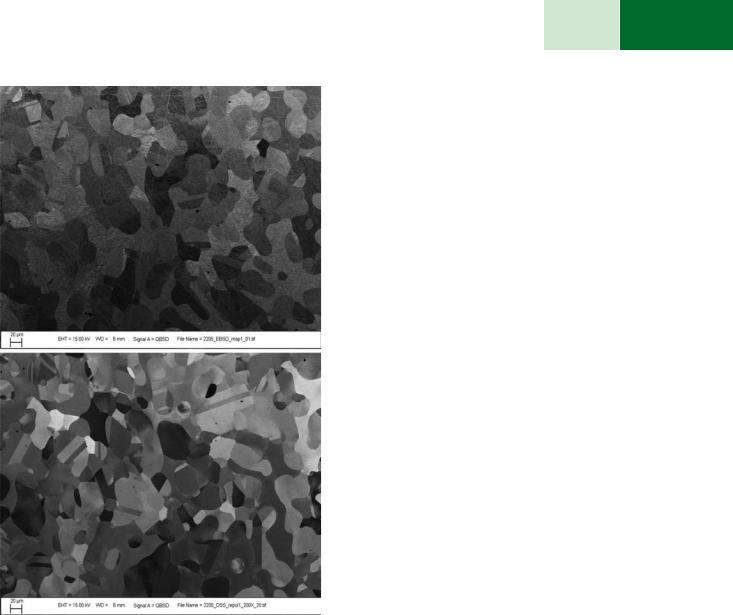
. Fig. 29.16 Backscattered electron images of metallographically polished dual phase steel for EBSD analysis. Short working distance backscattered imaging results in excellent crystallographic contrast. a Standard metallographic practice shows numerous fine scratches that are visible in channeling contrast. EBSD mapping is still possible but not optimal. b Standard practice plus 4 h of vibratory polishing on colloidal silica results in a higher-quality surface finish and optimal EBSD mapping (Bar = 20 µm)
instrumentation particulars) and a backscattered electron image obtained. These images are sensitive to the crystallography of the sample and the grain orientation will determine the backscatter coefficient leading to beautiful images of the sample grain structure. In many cases, subsurface scratches and other sample preparation artifacts will be visible in this type of image that is not seen in secondary electron images or optical microscopy. . Figure 29.16 is an example of a high-quality metallographically polished sample image of a dual phase stainless steel. Note that the sample as polished with no colloidal silica polishing exhibits a large number of subsurface scratches that limit the EBSD results. After colloidal polishing for a few hours the difference in surface condition is readily apparent. Generally, results like these are a good predictor of a successful EBSD analysis.
Align Sample in the SEM
After the sample is imaged and the sample preparation found to be of good quality, the sample orientation within the SEM must be considered. EBSD is often used to determine the texture or distribution of crystallographic orientations with respect to some external frame of reference related to the sample or how the sample was processed. A good example of this is when metal plates are produced by mechanical rolling. It is often desired to determine the texture of the sample with respect to the rolling direction, the transverse direction, or the plate normal direction. Or for the case where only one direction of the sample is expected to show a preferred texture, as in a wire where the preferred crystallographic direction lies along the wire axis, this axis should be mounted parallel to one of the primary directions in the SEM. Other times it is an assessment of the crystallographic growth direction and thus the sample should be carefully aligned so that the growth direction corresponds to one of the primary axes of the scanned image. Thus, the sample must be carefully aligned in the SEM, and one must be aware of the tilt axis of the SEM stage and the directions of the x- and y-stage movements (Britton et al. 2016).
Once the external reference directions have been set parallel to the microscope reference direction, then the sample still must be tilted for EBSD examination. For the best EBSD the sample must be tilted to about 70° with respect to the electron beam. This tilt is best performed with a view of the inside of the chamber with a video image so that the high tilt does not result in the sample contacting the microscope pole piece or other hard expensive components of the microscope. Once the sample is tilted to the appropriate angle and the area of interest brought under the electron beam then the EBSD camera must be moved into position. The best camera position is close to the sample so that the camera captures about 60–90° of the pattern. Also the brightest part of the pattern should be located about one third of the total camera area down from the top of the active area. This position will give the best possibility of good patterns being obtained.
Check for EBSD Patterns
Once the sample has been prepared appropriately and positioned correctly within the SEM, it is sensible to have a quick collection of a few randomly located points to ensure that good patterns can be obtained. This is the opportunity to optimize the SEM parameters for the acquisition. This is also an excellent opportunity to determine that the phases selected for indexing are chosen correctly. Correct completion of these steps will go a long way to ensure that a quality orientation map can be collected.
The first step is to select correct microscope parameters for EBSD acquisition. The accelerating voltage is not extremely critical for success but should be set somewhere between 10 and 20 kV depending on the sample that is to be analyzed. The other microscope-critical setting is the current in the electron beam. In general, the best choice is the highest beam current that the microscope can generate consistent

\504 Chapter 29 · Characterizing Crystalline Materials in the SEM
with the beam’s size not being larger than the features of interest within the sample. Modern EBSD cameras have been developed to be more sensitive and capable of dealing with lower beam currents. This in practice means that one should try settings that generate 1–2 nA as a starting point. Higher beam currents will be desirable for faster EBSD map acquisition. Once these conditions are set, a few patterns should be collected. If patterns are of poor quality it may be necessary to revisit the sample preparation steps used and modify them in order to reduce the surface damage. Although some fine
29 tuning of the microscope operating conditions may improve the pattern quality, microscope operating conditions cannot make up for poor quality patterns due to inadequate sample preparation.
If good quality patterns are obtained, it now an excellent time to determine that appropriate match units have been selected from a database of crystallographic structures. For the highest-quality EBSD work, one should try and calibrate the EBSD camera geometry for each experiment. Modern systems will use one of the known phases from the sample (if you have a known phase) and the crystallographic data file selected to try and index one or multiple diffraction patterns. Once a match has been found, the software will attempt to vary the calibration parameters to select the parameters that give the best fit to the observed EBSD pattern. Once this is done one can assume the system is adequately calibrated. It is recommended though that multiple points be tried to make sure calibration is optimal.
As discussed, EBSD is not a method that is routinely used to determine the crystal structure of the sample, although there has been work in this area, but it is a method that requires suitable match units to successfully index the EBSD patterns. Excellent quality EBSD patterns will not be indexed if an incorrect candidate unit cell has been selected. One should attempt to index a few of the patterns obtained from the sample with the selected candidate unit cells. If indexing is not possible, then it may be necessary to change the candidate unit cell and attempt indexing. In the case of a multi- phase sample it is important to collect patterns from all of the phases and insure that they can be indexed from the list of candidate unit cells.
Adjust SEM and Select EBSD Map Parameters
The analysis is now at the point where the quality of the EBSD patterns and therefore the sample preparation has been assessed and found to be adequate. The sample has been correctly positioned within the microscope with respect to collecting data that is referenced to the sample and the microscope operating conditions have been optimized. The
EBSD collection is nearly ready to proceed with a few other details.
First, due to the high tilt of the sample it will be apparent at lower magnifications that the areas of the sample away from the focus point will be out of focus. The best way to
deal with this issue is the use of dynamic focus as discussed elsewhere in this book. In brief, the dynamic focus adjusts the focus so that the electron beam focus is changed with respect to the position of the electron beam on the sample. This is of most importance for low magnification detailed scans but may still provide some advantages at higher magnifications as well. Once the dynamic focus has been properly set up, one can collect the desired SEM images of the sample.
EBSD is useful for a range of samples that include electrical conductors, like metals through electrically insulating oxide. For insulating samples or metal samples mounted for metallography, methods must be employed to reduce charging of the sample. Sample charging is an important issue as charging in the extreme can result in pattern distortions to the point that the patterns are no longer useful and if only a minor effect sample drift may result causing the resulting images and maps to be distorted. It is sometimes adequate to sputter coat samples to ensure conductivity. However, this coating should be kept as thin as possible and it is best to use metal films rather than carbon coating as the conductivity of metal coating are usually much higher. If the sample cannot be coated there is another approach that has been found to be quite useful and that is the use of variable pressure in the sample chamber. The introduction of a low pressure, generally only a few 10–20 Pa, is required to reduce charging effects for EBSD. If a pressure that is too high is utilized there will be a noticeable degradation of the pattern quality due to scattering of the electrons between the sample and the phosphor screen. Thus, some trial and error may be required to set the conditions correctly (El-Dasher and Torres 2009).
There is no absolutely correct way to set up EBSD map parameters due to the variety of sample types and the information that may be required. There are a few simple things that can be done to ensure that quality orientation data are collected. One, the most important is to determine the step size that will be used for the EBSD map. If too large of a step size is selected, important details of the microstructure may be missed; and conversely if too fine of a step size is used, the resulting maps may be of high quality but will have taken much longer to acquire than if a larger step size had been selected. One strategy for an unknown sample is to start with a coarse step size so that a rather quick map can be obtained and allow better sampling strategies to be developed. The large step size map will allow the user to determine if the candidate match phase or phases are appropriate, get an estimate of the grain size and to begin to visualize the microstructure of the sample. The large-step-size image will then allow a better selection of step size for more detailed studies. One rule of thumb is that at least 10 points across the diameter of a grain are required for a reasonable assessment of the grain size.