

- •Preface
- •Imaging Microscopic Features
- •Measuring the Crystal Structure
- •References
- •Contents
- •1.4 Simulating the Effects of Elastic Scattering: Monte Carlo Calculations
- •What Are the Main Features of the Beam Electron Interaction Volume?
- •How Does the Interaction Volume Change with Composition?
- •How Does the Interaction Volume Change with Incident Beam Energy?
- •How Does the Interaction Volume Change with Specimen Tilt?
- •1.5 A Range Equation To Estimate the Size of the Interaction Volume
- •References
- •2: Backscattered Electrons
- •2.1 Origin
- •2.2.1 BSE Response to Specimen Composition (η vs. Atomic Number, Z)
- •SEM Image Contrast with BSE: “Atomic Number Contrast”
- •SEM Image Contrast: “BSE Topographic Contrast—Number Effects”
- •2.2.3 Angular Distribution of Backscattering
- •Beam Incident at an Acute Angle to the Specimen Surface (Specimen Tilt > 0°)
- •SEM Image Contrast: “BSE Topographic Contrast—Trajectory Effects”
- •2.2.4 Spatial Distribution of Backscattering
- •Depth Distribution of Backscattering
- •Radial Distribution of Backscattered Electrons
- •2.3 Summary
- •References
- •3: Secondary Electrons
- •3.1 Origin
- •3.2 Energy Distribution
- •3.3 Escape Depth of Secondary Electrons
- •3.8 Spatial Characteristics of Secondary Electrons
- •References
- •4: X-Rays
- •4.1 Overview
- •4.2 Characteristic X-Rays
- •4.2.1 Origin
- •4.2.2 Fluorescence Yield
- •4.2.3 X-Ray Families
- •4.2.4 X-Ray Nomenclature
- •4.2.6 Characteristic X-Ray Intensity
- •Isolated Atoms
- •X-Ray Production in Thin Foils
- •X-Ray Intensity Emitted from Thick, Solid Specimens
- •4.3 X-Ray Continuum (bremsstrahlung)
- •4.3.1 X-Ray Continuum Intensity
- •4.3.3 Range of X-ray Production
- •4.4 X-Ray Absorption
- •4.5 X-Ray Fluorescence
- •References
- •5.1 Electron Beam Parameters
- •5.2 Electron Optical Parameters
- •5.2.1 Beam Energy
- •Landing Energy
- •5.2.2 Beam Diameter
- •5.2.3 Beam Current
- •5.2.4 Beam Current Density
- •5.2.5 Beam Convergence Angle, α
- •5.2.6 Beam Solid Angle
- •5.2.7 Electron Optical Brightness, β
- •Brightness Equation
- •5.2.8 Focus
- •Astigmatism
- •5.3 SEM Imaging Modes
- •5.3.1 High Depth-of-Field Mode
- •5.3.2 High-Current Mode
- •5.3.3 Resolution Mode
- •5.3.4 Low-Voltage Mode
- •5.4 Electron Detectors
- •5.4.1 Important Properties of BSE and SE for Detector Design and Operation
- •Abundance
- •Angular Distribution
- •Kinetic Energy Response
- •5.4.2 Detector Characteristics
- •Angular Measures for Electron Detectors
- •Elevation (Take-Off) Angle, ψ, and Azimuthal Angle, ζ
- •Solid Angle, Ω
- •Energy Response
- •Bandwidth
- •5.4.3 Common Types of Electron Detectors
- •Backscattered Electrons
- •Passive Detectors
- •Scintillation Detectors
- •Semiconductor BSE Detectors
- •5.4.4 Secondary Electron Detectors
- •Everhart–Thornley Detector
- •Through-the-Lens (TTL) Electron Detectors
- •TTL SE Detector
- •TTL BSE Detector
- •Measuring the DQE: BSE Semiconductor Detector
- •References
- •6: Image Formation
- •6.1 Image Construction by Scanning Action
- •6.2 Magnification
- •6.3 Making Dimensional Measurements With the SEM: How Big Is That Feature?
- •Using a Calibrated Structure in ImageJ-Fiji
- •6.4 Image Defects
- •6.4.1 Projection Distortion (Foreshortening)
- •6.4.2 Image Defocusing (Blurring)
- •6.5 Making Measurements on Surfaces With Arbitrary Topography: Stereomicroscopy
- •6.5.1 Qualitative Stereomicroscopy
- •Fixed beam, Specimen Position Altered
- •Fixed Specimen, Beam Incidence Angle Changed
- •6.5.2 Quantitative Stereomicroscopy
- •Measuring a Simple Vertical Displacement
- •References
- •7: SEM Image Interpretation
- •7.1 Information in SEM Images
- •7.2.2 Calculating Atomic Number Contrast
- •Establishing a Robust Light-Optical Analogy
- •Getting It Wrong: Breaking the Light-Optical Analogy of the Everhart–Thornley (Positive Bias) Detector
- •Deconstructing the SEM/E–T Image of Topography
- •SUM Mode (A + B)
- •DIFFERENCE Mode (A−B)
- •References
- •References
- •9: Image Defects
- •9.1 Charging
- •9.1.1 What Is Specimen Charging?
- •9.1.3 Techniques to Control Charging Artifacts (High Vacuum Instruments)
- •Observing Uncoated Specimens
- •Coating an Insulating Specimen for Charge Dissipation
- •Choosing the Coating for Imaging Morphology
- •9.2 Radiation Damage
- •9.3 Contamination
- •References
- •10: High Resolution Imaging
- •10.2 Instrumentation Considerations
- •10.4.1 SE Range Effects Produce Bright Edges (Isolated Edges)
- •10.4.4 Too Much of a Good Thing: The Bright Edge Effect Hinders Locating the True Position of an Edge for Critical Dimension Metrology
- •10.5.1 Beam Energy Strategies
- •Low Beam Energy Strategy
- •High Beam Energy Strategy
- •Making More SE1: Apply a Thin High-δ Metal Coating
- •Making Fewer BSEs, SE2, and SE3 by Eliminating Bulk Scattering From the Substrate
- •10.6 Factors That Hinder Achieving High Resolution
- •10.6.2 Pathological Specimen Behavior
- •Contamination
- •Instabilities
- •References
- •11: Low Beam Energy SEM
- •11.3 Selecting the Beam Energy to Control the Spatial Sampling of Imaging Signals
- •11.3.1 Low Beam Energy for High Lateral Resolution SEM
- •11.3.2 Low Beam Energy for High Depth Resolution SEM
- •11.3.3 Extremely Low Beam Energy Imaging
- •References
- •12.1.1 Stable Electron Source Operation
- •12.1.2 Maintaining Beam Integrity
- •12.1.4 Minimizing Contamination
- •12.3.1 Control of Specimen Charging
- •12.5 VPSEM Image Resolution
- •References
- •13: ImageJ and Fiji
- •13.1 The ImageJ Universe
- •13.2 Fiji
- •13.3 Plugins
- •13.4 Where to Learn More
- •References
- •14: SEM Imaging Checklist
- •14.1.1 Conducting or Semiconducting Specimens
- •14.1.2 Insulating Specimens
- •14.2 Electron Signals Available
- •14.2.1 Beam Electron Range
- •14.2.2 Backscattered Electrons
- •14.2.3 Secondary Electrons
- •14.3 Selecting the Electron Detector
- •14.3.2 Backscattered Electron Detectors
- •14.3.3 “Through-the-Lens” Detectors
- •14.4 Selecting the Beam Energy for SEM Imaging
- •14.4.4 High Resolution SEM Imaging
- •Strategy 1
- •Strategy 2
- •14.5 Selecting the Beam Current
- •14.5.1 High Resolution Imaging
- •14.5.2 Low Contrast Features Require High Beam Current and/or Long Frame Time to Establish Visibility
- •14.6 Image Presentation
- •14.6.1 “Live” Display Adjustments
- •14.6.2 Post-Collection Processing
- •14.7 Image Interpretation
- •14.7.1 Observer’s Point of View
- •14.7.3 Contrast Encoding
- •14.8.1 VPSEM Advantages
- •14.8.2 VPSEM Disadvantages
- •15: SEM Case Studies
- •15.1 Case Study: How High Is That Feature Relative to Another?
- •15.2 Revealing Shallow Surface Relief
- •16.1.2 Minor Artifacts: The Si-Escape Peak
- •16.1.3 Minor Artifacts: Coincidence Peaks
- •16.1.4 Minor Artifacts: Si Absorption Edge and Si Internal Fluorescence Peak
- •16.2 “Best Practices” for Electron-Excited EDS Operation
- •16.2.1 Operation of the EDS System
- •Choosing the EDS Time Constant (Resolution and Throughput)
- •Choosing the Solid Angle of the EDS
- •Selecting a Beam Current for an Acceptable Level of System Dead-Time
- •16.3.1 Detector Geometry
- •16.3.2 Process Time
- •16.3.3 Optimal Working Distance
- •16.3.4 Detector Orientation
- •16.3.5 Count Rate Linearity
- •16.3.6 Energy Calibration Linearity
- •16.3.7 Other Items
- •16.3.8 Setting Up a Quality Control Program
- •Using the QC Tools Within DTSA-II
- •Creating a QC Project
- •Linearity of Output Count Rate with Live-Time Dose
- •Resolution and Peak Position Stability with Count Rate
- •Solid Angle for Low X-ray Flux
- •Maximizing Throughput at Moderate Resolution
- •References
- •17: DTSA-II EDS Software
- •17.1 Getting Started With NIST DTSA-II
- •17.1.1 Motivation
- •17.1.2 Platform
- •17.1.3 Overview
- •17.1.4 Design
- •Simulation
- •Quantification
- •Experiment Design
- •Modeled Detectors (. Fig. 17.1)
- •Window Type (. Fig. 17.2)
- •The Optimal Working Distance (. Figs. 17.3 and 17.4)
- •Elevation Angle
- •Sample-to-Detector Distance
- •Detector Area
- •Crystal Thickness
- •Number of Channels, Energy Scale, and Zero Offset
- •Resolution at Mn Kα (Approximate)
- •Azimuthal Angle
- •Gold Layer, Aluminum Layer, Nickel Layer
- •Dead Layer
- •Zero Strobe Discriminator (. Figs. 17.7 and 17.8)
- •Material Editor Dialog (. Figs. 17.9, 17.10, 17.11, 17.12, 17.13, and 17.14)
- •17.2.1 Introduction
- •17.2.2 Monte Carlo Simulation
- •17.2.4 Optional Tables
- •References
- •18: Qualitative Elemental Analysis by Energy Dispersive X-Ray Spectrometry
- •18.1 Quality Assurance Issues for Qualitative Analysis: EDS Calibration
- •18.2 Principles of Qualitative EDS Analysis
- •Exciting Characteristic X-Rays
- •Fluorescence Yield
- •X-ray Absorption
- •Si Escape Peak
- •Coincidence Peaks
- •18.3 Performing Manual Qualitative Analysis
- •Beam Energy
- •Choosing the EDS Resolution (Detector Time Constant)
- •Obtaining Adequate Counts
- •18.4.1 Employ the Available Software Tools
- •18.4.3 Lower Photon Energy Region
- •18.4.5 Checking Your Work
- •18.5 A Worked Example of Manual Peak Identification
- •References
- •19.1 What Is a k-ratio?
- •19.3 Sets of k-ratios
- •19.5 The Analytical Total
- •19.6 Normalization
- •19.7.1 Oxygen by Assumed Stoichiometry
- •19.7.3 Element by Difference
- •19.8 Ways of Reporting Composition
- •19.8.1 Mass Fraction
- •19.8.2 Atomic Fraction
- •19.8.3 Stoichiometry
- •19.8.4 Oxide Fractions
- •Example Calculations
- •19.9 The Accuracy of Quantitative Electron-Excited X-ray Microanalysis
- •19.9.1 Standards-Based k-ratio Protocol
- •19.9.2 “Standardless Analysis”
- •19.10 Appendix
- •19.10.1 The Need for Matrix Corrections To Achieve Quantitative Analysis
- •19.10.2 The Physical Origin of Matrix Effects
- •19.10.3 ZAF Factors in Microanalysis
- •X-ray Generation With Depth, φ(ρz)
- •X-ray Absorption Effect, A
- •X-ray Fluorescence, F
- •References
- •20.2 Instrumentation Requirements
- •20.2.1 Choosing the EDS Parameters
- •EDS Spectrum Channel Energy Width and Spectrum Energy Span
- •EDS Time Constant (Resolution and Throughput)
- •EDS Calibration
- •EDS Solid Angle
- •20.2.2 Choosing the Beam Energy, E0
- •20.2.3 Measuring the Beam Current
- •20.2.4 Choosing the Beam Current
- •Optimizing Analysis Strategy
- •20.3.4 Ba-Ti Interference in BaTiSi3O9
- •20.4 The Need for an Iterative Qualitative and Quantitative Analysis Strategy
- •20.4.2 Analysis of a Stainless Steel
- •20.5 Is the Specimen Homogeneous?
- •20.6 Beam-Sensitive Specimens
- •20.6.1 Alkali Element Migration
- •20.6.2 Materials Subject to Mass Loss During Electron Bombardment—the Marshall-Hall Method
- •Thin Section Analysis
- •Bulk Biological and Organic Specimens
- •References
- •21: Trace Analysis by SEM/EDS
- •21.1 Limits of Detection for SEM/EDS Microanalysis
- •21.2.1 Estimating CDL from a Trace or Minor Constituent from Measuring a Known Standard
- •21.2.2 Estimating CDL After Determination of a Minor or Trace Constituent with Severe Peak Interference from a Major Constituent
- •21.3 Measurements of Trace Constituents by Electron-Excited Energy Dispersive X-ray Spectrometry
- •The Inevitable Physics of Remote Excitation Within the Specimen: Secondary Fluorescence Beyond the Electron Interaction Volume
- •Simulation of Long-Range Secondary X-ray Fluorescence
- •NIST DTSA II Simulation: Vertical Interface Between Two Regions of Different Composition in a Flat Bulk Target
- •NIST DTSA II Simulation: Cubic Particle Embedded in a Bulk Matrix
- •21.5 Summary
- •References
- •22.1.2 Low Beam Energy Analysis Range
- •22.2 Advantage of Low Beam Energy X-Ray Microanalysis
- •22.2.1 Improved Spatial Resolution
- •22.3 Challenges and Limitations of Low Beam Energy X-Ray Microanalysis
- •22.3.1 Reduced Access to Elements
- •22.3.3 At Low Beam Energy, Almost Everything Is Found To Be Layered
- •Analysis of Surface Contamination
- •References
- •23: Analysis of Specimens with Special Geometry: Irregular Bulk Objects and Particles
- •23.2.1 No Chemical Etching
- •23.3 Consequences of Attempting Analysis of Bulk Materials With Rough Surfaces
- •23.4.1 The Raw Analytical Total
- •23.4.2 The Shape of the EDS Spectrum
- •23.5 Best Practices for Analysis of Rough Bulk Samples
- •23.6 Particle Analysis
- •Particle Sample Preparation: Bulk Substrate
- •The Importance of Beam Placement
- •Overscanning
- •“Particle Mass Effect”
- •“Particle Absorption Effect”
- •The Analytical Total Reveals the Impact of Particle Effects
- •Does Overscanning Help?
- •23.6.6 Peak-to-Background (P/B) Method
- •Specimen Geometry Severely Affects the k-ratio, but Not the P/B
- •Using the P/B Correspondence
- •23.7 Summary
- •References
- •24: Compositional Mapping
- •24.2 X-Ray Spectrum Imaging
- •24.2.1 Utilizing XSI Datacubes
- •24.2.2 Derived Spectra
- •SUM Spectrum
- •MAXIMUM PIXEL Spectrum
- •24.3 Quantitative Compositional Mapping
- •24.4 Strategy for XSI Elemental Mapping Data Collection
- •24.4.1 Choosing the EDS Dead-Time
- •24.4.2 Choosing the Pixel Density
- •24.4.3 Choosing the Pixel Dwell Time
- •“Flash Mapping”
- •High Count Mapping
- •References
- •25.1 Gas Scattering Effects in the VPSEM
- •25.1.1 Why Doesn’t the EDS Collimator Exclude the Remote Skirt X-Rays?
- •25.2 What Can Be Done To Minimize gas Scattering in VPSEM?
- •25.2.2 Favorable Sample Characteristics
- •Particle Analysis
- •25.2.3 Unfavorable Sample Characteristics
- •References
- •26.1 Instrumentation
- •26.1.2 EDS Detector
- •26.1.3 Probe Current Measurement Device
- •Direct Measurement: Using a Faraday Cup and Picoammeter
- •A Faraday Cup
- •Electrically Isolated Stage
- •Indirect Measurement: Using a Calibration Spectrum
- •26.1.4 Conductive Coating
- •26.2 Sample Preparation
- •26.2.1 Standard Materials
- •26.2.2 Peak Reference Materials
- •26.3 Initial Set-Up
- •26.3.1 Calibrating the EDS Detector
- •Selecting a Pulse Process Time Constant
- •Energy Calibration
- •Quality Control
- •Sample Orientation
- •Detector Position
- •Probe Current
- •26.4 Collecting Data
- •26.4.1 Exploratory Spectrum
- •26.4.2 Experiment Optimization
- •26.4.3 Selecting Standards
- •26.4.4 Reference Spectra
- •26.4.5 Collecting Standards
- •26.4.6 Collecting Peak-Fitting References
- •26.5 Data Analysis
- •26.5.2 Quantification
- •26.6 Quality Check
- •Reference
- •27.2 Case Study: Aluminum Wire Failures in Residential Wiring
- •References
- •28: Cathodoluminescence
- •28.1 Origin
- •28.2 Measuring Cathodoluminescence
- •28.3 Applications of CL
- •28.3.1 Geology
- •Carbonado Diamond
- •Ancient Impact Zircons
- •28.3.2 Materials Science
- •Semiconductors
- •Lead-Acid Battery Plate Reactions
- •28.3.3 Organic Compounds
- •References
- •29.1.1 Single Crystals
- •29.1.2 Polycrystalline Materials
- •29.1.3 Conditions for Detecting Electron Channeling Contrast
- •Specimen Preparation
- •Instrument Conditions
- •29.2.1 Origin of EBSD Patterns
- •29.2.2 Cameras for EBSD Pattern Detection
- •29.2.3 EBSD Spatial Resolution
- •29.2.5 Steps in Typical EBSD Measurements
- •Sample Preparation for EBSD
- •Align Sample in the SEM
- •Check for EBSD Patterns
- •Adjust SEM and Select EBSD Map Parameters
- •Run the Automated Map
- •29.2.6 Display of the Acquired Data
- •29.2.7 Other Map Components
- •29.2.10 Application Example
- •Application of EBSD To Understand Meteorite Formation
- •29.2.11 Summary
- •Specimen Considerations
- •EBSD Detector
- •Selection of Candidate Crystallographic Phases
- •Microscope Operating Conditions and Pattern Optimization
- •Selection of EBSD Acquisition Parameters
- •Collect the Orientation Map
- •References
- •30.1 Introduction
- •30.2 Ion–Solid Interactions
- •30.3 Focused Ion Beam Systems
- •30.5 Preparation of Samples for SEM
- •30.5.1 Cross-Section Preparation
- •30.5.2 FIB Sample Preparation for 3D Techniques and Imaging
- •30.6 Summary
- •References
- •31: Ion Beam Microscopy
- •31.1 What Is So Useful About Ions?
- •31.2 Generating Ion Beams
- •31.3 Signal Generation in the HIM
- •31.5 Patterning with Ion Beams
- •31.7 Chemical Microanalysis with Ion Beams
- •References
- •Appendix
- •A Database of Electron–Solid Interactions
- •A Database of Electron–Solid Interactions
- •Introduction
- •Backscattered Electrons
- •Secondary Yields
- •Stopping Powers
- •X-ray Ionization Cross Sections
- •Conclusions
- •References
- •Index
- •Reference List
- •Index
\446 Chapter 25 · Attempting Electron-Excited X-Ray Microanalysis in the Variable Pressure Scanning Electron Microscope (VPSEM)
25 |
|
80768 |
Ch#: |
|
ChkV: |
|
Work: 6120 |
Results: 3172 |
Marker: |
|
|
|
|
|
|
|
||
|
170 |
1.7000 |
|
|
|
|
||||||||||||
|
Si |
14 |
|
|
500 µm 40Cu-60Au |
|
||||||||||||
|
|
|
AlKα |
AuMα |
|
|
|
|
|
|
|
|
|
|||||
|
|
|
|
|
|
|
|
|
|
|
|
|||||||
|
|
|
|
Spec# |
Counts |
|
|
|
|
|
|
|
|
|||||
|
|
|
|
|
|
|
|
|
1 |
6602 |
|
|
|
|
|
|
|
|
|
|
|
|
|
|
|
|
|
2 |
8435 |
|
|
|
|
|
|
|
|
|
|
|
|
|
|
|
|
|
3 |
4632 |
|
|
|
|
|
25 mm AI |
|
|
|
|
|
|
|
|
|
|
|
4 |
4936 |
|
|
|
|
|
|
|
|
|
|
|
|
|
|
|
|
|
5 |
4330 |
|
|
|
|
|
|
|
|
|
|
|
|
|
|
|
|
|
6 |
4685 |
|
|
|
|
|
|
|
|
|
|
|
|
|
|
|
1600 Pa (12 torr) |
|
|
|
|
|
|
|
|
|
||
|
|
|
|
|
|
|
1200 Pa (9 torr) |
|
|
|
|
|
|
CuKα |
|
|
||
|
|
|
|
|
|
|
1000 Pa (7.5 torr) |
|
|
|
|
|
|
|
|
|
||
|
|
|
|
|
|
|
800 Pa (6 torr) |
|
|
|
GPL = 4 mm |
|
|
|
|
|||
|
|
|
|
|
|
|
|
|
|
|
|
|
|
|
|
|
||
|
|
|
|
|
|
|
600 Pa (4.5 torr) |
|
|
|
Water vapor |
|
|
|
|
|||
|
|
|
|
|
|
|
400 Pa (3 torr) |
|
|
|
E0 = 20 keV |
|
|
|
|
|||
|
|
|
|
|
|
|
133 Pa (1.5 torr) |
|
|
|
Scaled to AuM |
|
|
|
||||
|
|
|
|
CuLα1 |
|
|
|
|
|
|
|
|
|
|
||||
|
|
|
|
|
53 Pa (0.4 torr) |
|
|
|
|
|
|
|
|
|
||||
|
|
|
|
|
|
|
|
|
|
|
|
|
|
|
AuLα1 |
|||
|
|
|
|
|
|
|
|
|
|
|
|
|
|
|
|
|
|
|
|
|
|
|
|
|
|
|
|
|
|
|
|
FeKα |
|
|
CuKβ1 |
|
|
|
|
0 |
Kα |
|
|
|
|
|
|
|
|
|
|
|
||||
|
|
|
|
|
|
|
|
|
|
|
|
|
|
|
|
AuLι |
|
Α |
|
|
0.00 |
1.00 |
|
2.00 |
3.00 |
4.00 |
5.00 |
|
|
6.00 |
|
7.00 |
8.00 |
9.00 |
10.00 |
||
|
|
|
|
|
|
|
|
Photon energy (keV) |
|
|
|
|
|
|
||||
|
|
|
|
|
|
|
|
|
|
|
|
|
|
|
|
|
|
|
. Fig. 25.6 EDS spectra measured with the beam placed in the center of a 500 μm diameter wire of 40 wt % Cu–60 wt %Au surrounded by a 2.5-cm-diameter Al disk; E0 = 20 keV; gas path length = 4 mm; oxygen at various pressures
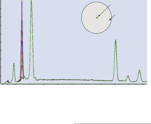
4 mm through water vapor, the EDS spectra measured over a pressure range from 53 Pa to 1600 Pa are superimposed, showing the in-growth of the Al peak with increasing pressure. Even at 53 Pa, a detectable Al peak is observed, despite the beam center being 250 μm away from the Al. As the pressure is increased, the Al peak ranges from an apparent trace to minor and finally major constituent peak.
DTSA-II also simulates the composite spectrum created by these two classes of electrons as they strike the specimen. Various configurations of two different materials can be specified, one that the unscattered beam strikes, for example, a particle, and the other by the skirt electrons, for example, the surrounding matrix. . Figure 25.7 shows spectra simulated for the example of . Fig. 25.6, the 500-μm-diameter 40 wt %Cu–60 wt %Au wire in the Al disk with a 4-mm-gas path length through water vapor. The simulation of the lowest VPSEM gas pressure of 53 Pa produces a low level Al peak similar to the experimental measurement. Thus, even at this low pressure and short gas path length for which 89 % of the electrons remain in the focused beam, there are still gas-scattered electrons falling at least 250 μm from the beam impact. As the pressure is progressively increased, the in-growth of the Al peak due to the skirt electrons is well modeled by the Monte Carlo simulation.
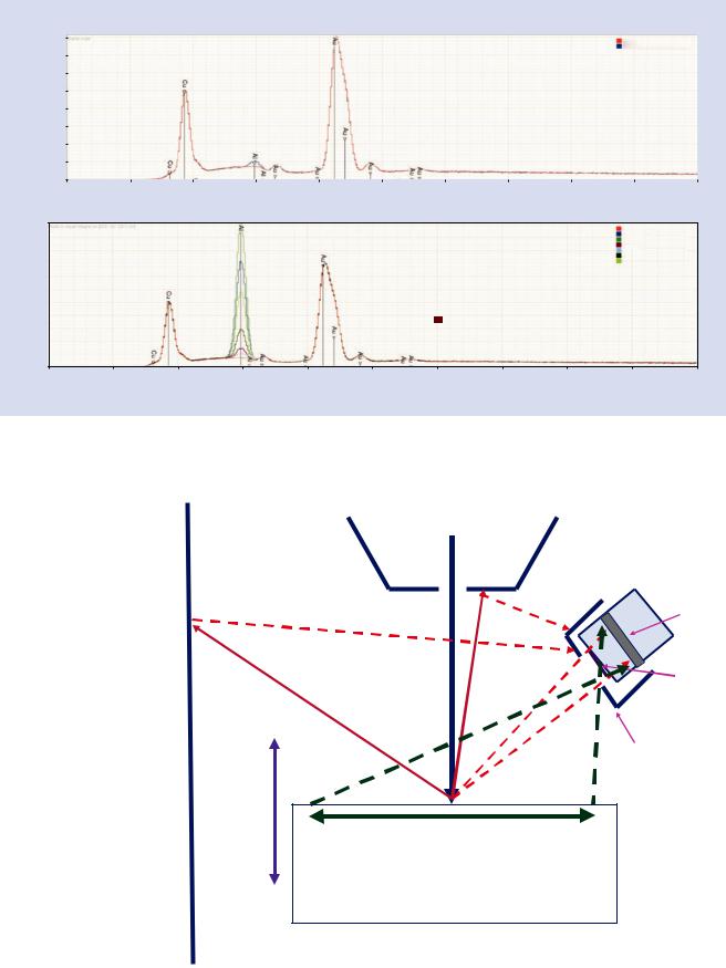
25.1.1\ Why Doesn’t the EDS Collimator Exclude the Remote Skirt X-Rays?
Gas scattering in the VPSEM mode always degrades the incident beam, transferring a significant fraction of the beam electrons into the skirt. The radius of the skirt can reach a millimeter or more from the focused beam impact. It might be thought that the EDS collimator would restrict the acceptance area of the EDS to exclude most of the skirt. As shown in the schematic diagram in . Fig. 25.8, while a simple collimator acts to successfully shield the EDS from accepting X-rays produced by backscattered electrons striking the lens and chamber walls, the acceptance volume near the column optic axis is quite large. The EDS acceptance is not defined by looking back at the detector from the specimen space as the cone of rays whose apex is at the beam impact on the specimen and whose base is the detector active area (the dashed red lines in
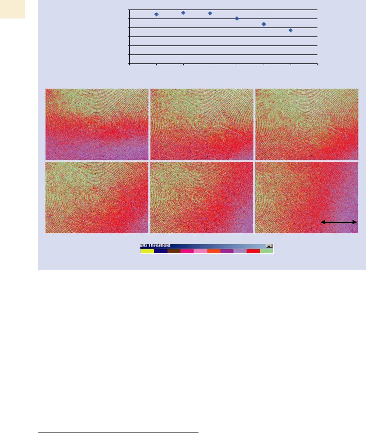
. Fig. 25.8). While the red lines define the solid angle of the detector for emission from the beam impact point, the acceptance region is actually defined by looking from the detector through the collimator at the specimen space (the dashed green lines in . Fig. 25.8). The true area of acceptance can be readily determined by conducting X-ray mapping measurements. . Fig. 25.9 shows a series of measurements of X-ray maps of a machined Al disk taken at the lowest available
25.1 ·
Counts
Gas Scattering Effects in the VPSEM |
|
|
|
|
|
|
447 |
|
25 |
||||
|
|
|
|
|
|
|
|
|
|
||||
16000 |
|
|
|
|
DTSA-II Monte Carlo simulation |
|
|
|
|
|
|
||
|
|
|
|
|
|
|
|
|
|
|
|||
|
|
|
|
|
40Cu-60Au |
|
|
High_vacum_40Cu-60Au_20keV |
|
||||
14000 |
|
|
|
|
|
|
|
|
53Pa_H2O_40Cu-60Au_20keV16x |
|
|||
|
|
|
|
|
|
E0 = 20 keV |
|
|
|
|
|
|
|
12000 |
|
|
|
|
|
|
|
|
|
|
|
|
|
|
|
|
|
|
|
4 mm gas path length |
|
|
|
|
|
||
10000 |
|
|
|
|
|
|
|
|
|
|
|
||
|
|
|
|
|
|
|
|
|
|
|
|
|
|
8000 |
|
|
|
|
|
|
H2O |
|
|
|
|
|
|
6000 |
|
|
|
|
|
|
|
|
|
|
|
|
|
4000 |
|
|
|
|
|
|
|
53 Pa H2O |
|
|
|
|
|
|
|
|
|
|
|
|
High vacuum |
|
|
|
|
|
|
2000 |
|
|
|
|
|
|
|
|
|
|
|
|
|
|
|
|
|
|
|
|
|
|
|
|
|
|
|
0 |
|
|
|
|
|
|
|
|
|
|
|
|
|
0 |
500 |
1000 |
1500 |
2000 |
2500 |
3000 |
3500 |
4000 |
4500 |
|
5000 |
||
Photon energy (eV)
Relative Counts
1600 Pa H2O
1200 Pa H2O
800 Pa H2O
400 Pa H2O
133 Pa H2O
53 Pa H2O High vacuum
High_vacum_40Cu-60Au_20keV
1200Pa_H2O_40Cu-60Au_20keV 1600Pa_H2O_40Cu-60Au_20keV 133Pa_H2O_40Cu-60Au_20keV 53Pa_H2O_40Cu-60Au_20keV16x 400Pa_H2O_40Cu-60Au_20keV 800Pa_H2O_40Cu-60Au_20keV
Scaled to AuM
0 |
500 |
1000 |
1500 |
2000 |
2500 |
3000 |
3500 |
4000 |
4500 |
5000 |
|
|
|
|
Photon energy (eV) |
|
|
|
|
|
|
. Fig. 25.7 DTSA-II Monte Carlo simulations of the specimen and gas scattering conditions of . Fig. 25.6. Upper plot: high vacuum and 53 Pa (4 mm GPL, H2O). Lower plot: high vacuum and various pressures from 53 Pa to 1600 Pa
. Fig. 25.8 Schematic diagram showing the acceptance area of the EDS collimator
Chamber
wall
Final lens
Remote X-rays |
EDS |
|
detector |
||
|
|
|
Window |
|
BSE |
|
|
BSE |
|
|
|
Collimator & |
|
|
electron trap |
mm |
|
Specimen X-rays |
|
Green = |
|
Several |
|
|
|
Extent of |
|
Several mm |
specimen |
|
|
X-ray sources |
|
|
|
|
|
|
NOT excluded |
|
|
by collimator |
\448 Chapter 25 · Attempting Electron-Excited X-Ray Microanalysis in the Variable Pressure Scanning Electron Microscope (VPSEM)
25 1200
Al counts/pixel
1000
800
600
400
200
0
8 |
10 |
12 |
14 |
16 |
18 |
20 |
22 |
|
|
|
Working distance (mm) |
|
|
|
|
10 mm |
12 mm |
14 mm |
16 mm |
18 mm |
20 mm |
1 mm
Al machined surface
0 |
10 |
20 |
30 |
40 |
50 |
60 |
70 |
80 |
90 |
100 |
. Fig. 25.9 Collimator acceptance volume as determined by mapping an Al disk at various working distances (10–20 mm) at the widest scanned field (i.e., lowest magnification); the plot shows the
intensity measured at the center of the scan field as a function of working distance
magnification (largest scan field) over a series of working distances. The false color scale shows the while the intensity is not uniform within a map, it generally varies by less than 30% over the full map, a distance of millimeters, and moreover, as the maps are measured at different working distances, there is only about 30% variation over the vertical range, which is confirmed by the plot of the intensity measured at the center of each map. Thus, X-rays generated throughout a large volume are accepted through the collimator by the EDS so that collimation provides virtually no relief from the effects of remote X-ray generation caused by gas scattering in the VPSEM.
25.1.2\ Other Artifacts Observed in VPSEM
X-Ray Spectrometry
Inelastic scattering of the beam electrons and backscattered electrons with the atoms of the environmental gas causes
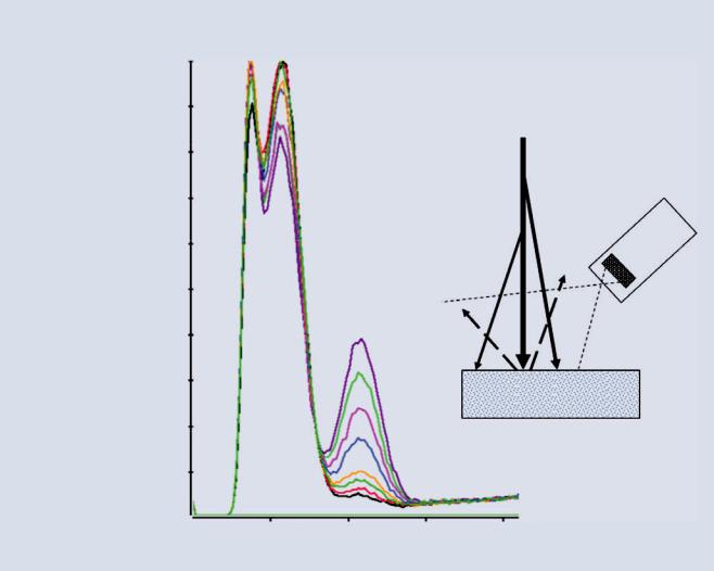
inner shell ionization leading to X-ray emission that contributes to the measured spectrum. The density of gas atoms (number/unit volume) is orders of magnitude lower than the density in the solid specimen, but the distance that the beam travels in the gas is orders of magnitude longer than it travels in the solid. The contribution of the environmental gas is illustrated for a simple experiment in . Fig. 25.10, where the beam strikes a carbon target at a series of different pressures. The in-growth of the oxygen peak from ionization of the water vapor used as the environmental gas can be seen. A detectable oxygen peak is seen for pressures of 133 Pa (1 torr) and higher for this particular gas path length (6 mm) and beam energy (20 keV). . Figure 25.11 shows an example of the contribution of the environmental gas to the spectrum measured from a 50 μm diameter glass shard with the composition listed in the figure placed on a carbon substrate. At the lower pressure (266 pA = 2 torr) for the gas path length used (3 mm), the footprint of the focused beam and skirt
25.1 · Gas Scattering Effects in the VPSEM
Extraneous X-ray peak(s) due to environmental gas
10455 |
Ch#: |
|
Chkv: |
|
Work: 476 |
Results:5 |
|||
53 |
0.5300 |
||||||||
|
|
|
|
C Ka |
|
|
|
||
|
|
|
|
|
|
|
|
|
Beam and BSE electrons |
E0 = 20 keV |
|
|
|
|
|
|
|
can ionize oxygen inner shell |
|
|
|
|
|
|
|
|
|
||
Gas = H2O |
|
|
|
|
|
|
|
H2O |
|
6 mm gas path |
|
|
|
Space# Counts |
|
||||
|
|
|
|
|
|||||
|
1 |
788 |
|
|
|||||
C disk, 25 mm diam |
|
2 |
924 |
|
|
||||
|
|
|
3 |
1523 |
|
|
|||
|
|
|
|
|
|||||
|
|
|
4 |
2129 |
|
|
|||
2000 Pa (15 torr) |
|
|
|
|
5 |
2753 |
|
|
|
|
|
|
|
6 |
3451 |
|
|
||
|
|
|
|
|
|||||
1600 Pa (12 torr) |
|
|
|
|
|
|
|
|
|
1200 Pa (9 torr) |
|
|
|
|
|
|
|
|
|
800 Pa (6 torr) |
|
|
|
|
|
O |
Ka |
|
|
|
|
|
|
|
|
|
|
|
|
400 Pa (3 torr) |
|
|
|
|
|
|
|
|
|
266 Pa (2 torr) |
|
|
|
|
|
|
|
|
Carbon |
|
|
|
|
|
|
|
|
|
|
133 Pa (1 torr) |
|
|
|
|
|
|
|
|
|
53 Pa (0.4 torr) |
|
|
|
|
|
|
|
|
|
|
|
|
|
|
|
|
|
|
|
0.00 |
0.25 |
0.50 |
0.75 |
1.00 |
|
|
Photon energy (keV) |
|
|
. Fig. 25.10 Generation of O K X-rays from the environmental gas as a function of chamber pressure
449 |
|
25 |
|
|
|
EDS
remain within the 50 μm diameter glass shard, as evidenced by the negligible C intensity in the spectrum. An O peak is also observed, at least some of which is actually from the specimen. When the pressure is increased by a factor of five to 1330 Pa (10 torr), the C intensity rises significantly because the skirt now extends beyond the boundary of the particle, and the O peak intensity increases by a factor of four, all of which is due to the environmental gas. It is also worth noting that in addition to characteristic X-rays from the environmental gas, there is increased bremsstrahlung generation as well from the inelastic scattering of beam and backscattered electrons with the gas atoms. In . Fig. 25.11, the background is substantially higher for the spectrum measured at the elevated pressure, leading to a reduced peak-to-background, which is easily seen for the Zn L-family and Al K-L2 peaks, an effect which makes for poorer limits of detection.
If the environmental gas can contribute to the spectrum, can the gas also absorb X-rays from the specimen?
Because of the low gas density, this effect might be expected to be negligible, and as listed in . Table 25.2, which is calculated for a 40 –mm-path through the gas from the X-ray source at the beam impact on the specimen to the EDS, for the lowest pressure considered, 10 Pa, over 99 % of the X-rays of all energies leaving the specimen in the direction of the detector arrive there, even for F K, the energy of which, 0.677 keV, is just above the O K-shell absorption energy, 0.535 keV, which results in a large mass absorption coefficient. When the pressure is increased to 100 Pa, the loss of F K due to absorption increases to ~ 6 %, and at a pressure of 2500 Pa (18.8 torr), ~ 80 % of the F K radiation is lost to gas absorption, and even Al K-L2 suffers a 20 % loss in intensity compared to the conventional high vacuum SEM situation.