

- •Preface
- •Imaging Microscopic Features
- •Measuring the Crystal Structure
- •References
- •Contents
- •1.4 Simulating the Effects of Elastic Scattering: Monte Carlo Calculations
- •What Are the Main Features of the Beam Electron Interaction Volume?
- •How Does the Interaction Volume Change with Composition?
- •How Does the Interaction Volume Change with Incident Beam Energy?
- •How Does the Interaction Volume Change with Specimen Tilt?
- •1.5 A Range Equation To Estimate the Size of the Interaction Volume
- •References
- •2: Backscattered Electrons
- •2.1 Origin
- •2.2.1 BSE Response to Specimen Composition (η vs. Atomic Number, Z)
- •SEM Image Contrast with BSE: “Atomic Number Contrast”
- •SEM Image Contrast: “BSE Topographic Contrast—Number Effects”
- •2.2.3 Angular Distribution of Backscattering
- •Beam Incident at an Acute Angle to the Specimen Surface (Specimen Tilt > 0°)
- •SEM Image Contrast: “BSE Topographic Contrast—Trajectory Effects”
- •2.2.4 Spatial Distribution of Backscattering
- •Depth Distribution of Backscattering
- •Radial Distribution of Backscattered Electrons
- •2.3 Summary
- •References
- •3: Secondary Electrons
- •3.1 Origin
- •3.2 Energy Distribution
- •3.3 Escape Depth of Secondary Electrons
- •3.8 Spatial Characteristics of Secondary Electrons
- •References
- •4: X-Rays
- •4.1 Overview
- •4.2 Characteristic X-Rays
- •4.2.1 Origin
- •4.2.2 Fluorescence Yield
- •4.2.3 X-Ray Families
- •4.2.4 X-Ray Nomenclature
- •4.2.6 Characteristic X-Ray Intensity
- •Isolated Atoms
- •X-Ray Production in Thin Foils
- •X-Ray Intensity Emitted from Thick, Solid Specimens
- •4.3 X-Ray Continuum (bremsstrahlung)
- •4.3.1 X-Ray Continuum Intensity
- •4.3.3 Range of X-ray Production
- •4.4 X-Ray Absorption
- •4.5 X-Ray Fluorescence
- •References
- •5.1 Electron Beam Parameters
- •5.2 Electron Optical Parameters
- •5.2.1 Beam Energy
- •Landing Energy
- •5.2.2 Beam Diameter
- •5.2.3 Beam Current
- •5.2.4 Beam Current Density
- •5.2.5 Beam Convergence Angle, α
- •5.2.6 Beam Solid Angle
- •5.2.7 Electron Optical Brightness, β
- •Brightness Equation
- •5.2.8 Focus
- •Astigmatism
- •5.3 SEM Imaging Modes
- •5.3.1 High Depth-of-Field Mode
- •5.3.2 High-Current Mode
- •5.3.3 Resolution Mode
- •5.3.4 Low-Voltage Mode
- •5.4 Electron Detectors
- •5.4.1 Important Properties of BSE and SE for Detector Design and Operation
- •Abundance
- •Angular Distribution
- •Kinetic Energy Response
- •5.4.2 Detector Characteristics
- •Angular Measures for Electron Detectors
- •Elevation (Take-Off) Angle, ψ, and Azimuthal Angle, ζ
- •Solid Angle, Ω
- •Energy Response
- •Bandwidth
- •5.4.3 Common Types of Electron Detectors
- •Backscattered Electrons
- •Passive Detectors
- •Scintillation Detectors
- •Semiconductor BSE Detectors
- •5.4.4 Secondary Electron Detectors
- •Everhart–Thornley Detector
- •Through-the-Lens (TTL) Electron Detectors
- •TTL SE Detector
- •TTL BSE Detector
- •Measuring the DQE: BSE Semiconductor Detector
- •References
- •6: Image Formation
- •6.1 Image Construction by Scanning Action
- •6.2 Magnification
- •6.3 Making Dimensional Measurements With the SEM: How Big Is That Feature?
- •Using a Calibrated Structure in ImageJ-Fiji
- •6.4 Image Defects
- •6.4.1 Projection Distortion (Foreshortening)
- •6.4.2 Image Defocusing (Blurring)
- •6.5 Making Measurements on Surfaces With Arbitrary Topography: Stereomicroscopy
- •6.5.1 Qualitative Stereomicroscopy
- •Fixed beam, Specimen Position Altered
- •Fixed Specimen, Beam Incidence Angle Changed
- •6.5.2 Quantitative Stereomicroscopy
- •Measuring a Simple Vertical Displacement
- •References
- •7: SEM Image Interpretation
- •7.1 Information in SEM Images
- •7.2.2 Calculating Atomic Number Contrast
- •Establishing a Robust Light-Optical Analogy
- •Getting It Wrong: Breaking the Light-Optical Analogy of the Everhart–Thornley (Positive Bias) Detector
- •Deconstructing the SEM/E–T Image of Topography
- •SUM Mode (A + B)
- •DIFFERENCE Mode (A−B)
- •References
- •References
- •9: Image Defects
- •9.1 Charging
- •9.1.1 What Is Specimen Charging?
- •9.1.3 Techniques to Control Charging Artifacts (High Vacuum Instruments)
- •Observing Uncoated Specimens
- •Coating an Insulating Specimen for Charge Dissipation
- •Choosing the Coating for Imaging Morphology
- •9.2 Radiation Damage
- •9.3 Contamination
- •References
- •10: High Resolution Imaging
- •10.2 Instrumentation Considerations
- •10.4.1 SE Range Effects Produce Bright Edges (Isolated Edges)
- •10.4.4 Too Much of a Good Thing: The Bright Edge Effect Hinders Locating the True Position of an Edge for Critical Dimension Metrology
- •10.5.1 Beam Energy Strategies
- •Low Beam Energy Strategy
- •High Beam Energy Strategy
- •Making More SE1: Apply a Thin High-δ Metal Coating
- •Making Fewer BSEs, SE2, and SE3 by Eliminating Bulk Scattering From the Substrate
- •10.6 Factors That Hinder Achieving High Resolution
- •10.6.2 Pathological Specimen Behavior
- •Contamination
- •Instabilities
- •References
- •11: Low Beam Energy SEM
- •11.3 Selecting the Beam Energy to Control the Spatial Sampling of Imaging Signals
- •11.3.1 Low Beam Energy for High Lateral Resolution SEM
- •11.3.2 Low Beam Energy for High Depth Resolution SEM
- •11.3.3 Extremely Low Beam Energy Imaging
- •References
- •12.1.1 Stable Electron Source Operation
- •12.1.2 Maintaining Beam Integrity
- •12.1.4 Minimizing Contamination
- •12.3.1 Control of Specimen Charging
- •12.5 VPSEM Image Resolution
- •References
- •13: ImageJ and Fiji
- •13.1 The ImageJ Universe
- •13.2 Fiji
- •13.3 Plugins
- •13.4 Where to Learn More
- •References
- •14: SEM Imaging Checklist
- •14.1.1 Conducting or Semiconducting Specimens
- •14.1.2 Insulating Specimens
- •14.2 Electron Signals Available
- •14.2.1 Beam Electron Range
- •14.2.2 Backscattered Electrons
- •14.2.3 Secondary Electrons
- •14.3 Selecting the Electron Detector
- •14.3.2 Backscattered Electron Detectors
- •14.3.3 “Through-the-Lens” Detectors
- •14.4 Selecting the Beam Energy for SEM Imaging
- •14.4.4 High Resolution SEM Imaging
- •Strategy 1
- •Strategy 2
- •14.5 Selecting the Beam Current
- •14.5.1 High Resolution Imaging
- •14.5.2 Low Contrast Features Require High Beam Current and/or Long Frame Time to Establish Visibility
- •14.6 Image Presentation
- •14.6.1 “Live” Display Adjustments
- •14.6.2 Post-Collection Processing
- •14.7 Image Interpretation
- •14.7.1 Observer’s Point of View
- •14.7.3 Contrast Encoding
- •14.8.1 VPSEM Advantages
- •14.8.2 VPSEM Disadvantages
- •15: SEM Case Studies
- •15.1 Case Study: How High Is That Feature Relative to Another?
- •15.2 Revealing Shallow Surface Relief
- •16.1.2 Minor Artifacts: The Si-Escape Peak
- •16.1.3 Minor Artifacts: Coincidence Peaks
- •16.1.4 Minor Artifacts: Si Absorption Edge and Si Internal Fluorescence Peak
- •16.2 “Best Practices” for Electron-Excited EDS Operation
- •16.2.1 Operation of the EDS System
- •Choosing the EDS Time Constant (Resolution and Throughput)
- •Choosing the Solid Angle of the EDS
- •Selecting a Beam Current for an Acceptable Level of System Dead-Time
- •16.3.1 Detector Geometry
- •16.3.2 Process Time
- •16.3.3 Optimal Working Distance
- •16.3.4 Detector Orientation
- •16.3.5 Count Rate Linearity
- •16.3.6 Energy Calibration Linearity
- •16.3.7 Other Items
- •16.3.8 Setting Up a Quality Control Program
- •Using the QC Tools Within DTSA-II
- •Creating a QC Project
- •Linearity of Output Count Rate with Live-Time Dose
- •Resolution and Peak Position Stability with Count Rate
- •Solid Angle for Low X-ray Flux
- •Maximizing Throughput at Moderate Resolution
- •References
- •17: DTSA-II EDS Software
- •17.1 Getting Started With NIST DTSA-II
- •17.1.1 Motivation
- •17.1.2 Platform
- •17.1.3 Overview
- •17.1.4 Design
- •Simulation
- •Quantification
- •Experiment Design
- •Modeled Detectors (. Fig. 17.1)
- •Window Type (. Fig. 17.2)
- •The Optimal Working Distance (. Figs. 17.3 and 17.4)
- •Elevation Angle
- •Sample-to-Detector Distance
- •Detector Area
- •Crystal Thickness
- •Number of Channels, Energy Scale, and Zero Offset
- •Resolution at Mn Kα (Approximate)
- •Azimuthal Angle
- •Gold Layer, Aluminum Layer, Nickel Layer
- •Dead Layer
- •Zero Strobe Discriminator (. Figs. 17.7 and 17.8)
- •Material Editor Dialog (. Figs. 17.9, 17.10, 17.11, 17.12, 17.13, and 17.14)
- •17.2.1 Introduction
- •17.2.2 Monte Carlo Simulation
- •17.2.4 Optional Tables
- •References
- •18: Qualitative Elemental Analysis by Energy Dispersive X-Ray Spectrometry
- •18.1 Quality Assurance Issues for Qualitative Analysis: EDS Calibration
- •18.2 Principles of Qualitative EDS Analysis
- •Exciting Characteristic X-Rays
- •Fluorescence Yield
- •X-ray Absorption
- •Si Escape Peak
- •Coincidence Peaks
- •18.3 Performing Manual Qualitative Analysis
- •Beam Energy
- •Choosing the EDS Resolution (Detector Time Constant)
- •Obtaining Adequate Counts
- •18.4.1 Employ the Available Software Tools
- •18.4.3 Lower Photon Energy Region
- •18.4.5 Checking Your Work
- •18.5 A Worked Example of Manual Peak Identification
- •References
- •19.1 What Is a k-ratio?
- •19.3 Sets of k-ratios
- •19.5 The Analytical Total
- •19.6 Normalization
- •19.7.1 Oxygen by Assumed Stoichiometry
- •19.7.3 Element by Difference
- •19.8 Ways of Reporting Composition
- •19.8.1 Mass Fraction
- •19.8.2 Atomic Fraction
- •19.8.3 Stoichiometry
- •19.8.4 Oxide Fractions
- •Example Calculations
- •19.9 The Accuracy of Quantitative Electron-Excited X-ray Microanalysis
- •19.9.1 Standards-Based k-ratio Protocol
- •19.9.2 “Standardless Analysis”
- •19.10 Appendix
- •19.10.1 The Need for Matrix Corrections To Achieve Quantitative Analysis
- •19.10.2 The Physical Origin of Matrix Effects
- •19.10.3 ZAF Factors in Microanalysis
- •X-ray Generation With Depth, φ(ρz)
- •X-ray Absorption Effect, A
- •X-ray Fluorescence, F
- •References
- •20.2 Instrumentation Requirements
- •20.2.1 Choosing the EDS Parameters
- •EDS Spectrum Channel Energy Width and Spectrum Energy Span
- •EDS Time Constant (Resolution and Throughput)
- •EDS Calibration
- •EDS Solid Angle
- •20.2.2 Choosing the Beam Energy, E0
- •20.2.3 Measuring the Beam Current
- •20.2.4 Choosing the Beam Current
- •Optimizing Analysis Strategy
- •20.3.4 Ba-Ti Interference in BaTiSi3O9
- •20.4 The Need for an Iterative Qualitative and Quantitative Analysis Strategy
- •20.4.2 Analysis of a Stainless Steel
- •20.5 Is the Specimen Homogeneous?
- •20.6 Beam-Sensitive Specimens
- •20.6.1 Alkali Element Migration
- •20.6.2 Materials Subject to Mass Loss During Electron Bombardment—the Marshall-Hall Method
- •Thin Section Analysis
- •Bulk Biological and Organic Specimens
- •References
- •21: Trace Analysis by SEM/EDS
- •21.1 Limits of Detection for SEM/EDS Microanalysis
- •21.2.1 Estimating CDL from a Trace or Minor Constituent from Measuring a Known Standard
- •21.2.2 Estimating CDL After Determination of a Minor or Trace Constituent with Severe Peak Interference from a Major Constituent
- •21.3 Measurements of Trace Constituents by Electron-Excited Energy Dispersive X-ray Spectrometry
- •The Inevitable Physics of Remote Excitation Within the Specimen: Secondary Fluorescence Beyond the Electron Interaction Volume
- •Simulation of Long-Range Secondary X-ray Fluorescence
- •NIST DTSA II Simulation: Vertical Interface Between Two Regions of Different Composition in a Flat Bulk Target
- •NIST DTSA II Simulation: Cubic Particle Embedded in a Bulk Matrix
- •21.5 Summary
- •References
- •22.1.2 Low Beam Energy Analysis Range
- •22.2 Advantage of Low Beam Energy X-Ray Microanalysis
- •22.2.1 Improved Spatial Resolution
- •22.3 Challenges and Limitations of Low Beam Energy X-Ray Microanalysis
- •22.3.1 Reduced Access to Elements
- •22.3.3 At Low Beam Energy, Almost Everything Is Found To Be Layered
- •Analysis of Surface Contamination
- •References
- •23: Analysis of Specimens with Special Geometry: Irregular Bulk Objects and Particles
- •23.2.1 No Chemical Etching
- •23.3 Consequences of Attempting Analysis of Bulk Materials With Rough Surfaces
- •23.4.1 The Raw Analytical Total
- •23.4.2 The Shape of the EDS Spectrum
- •23.5 Best Practices for Analysis of Rough Bulk Samples
- •23.6 Particle Analysis
- •Particle Sample Preparation: Bulk Substrate
- •The Importance of Beam Placement
- •Overscanning
- •“Particle Mass Effect”
- •“Particle Absorption Effect”
- •The Analytical Total Reveals the Impact of Particle Effects
- •Does Overscanning Help?
- •23.6.6 Peak-to-Background (P/B) Method
- •Specimen Geometry Severely Affects the k-ratio, but Not the P/B
- •Using the P/B Correspondence
- •23.7 Summary
- •References
- •24: Compositional Mapping
- •24.2 X-Ray Spectrum Imaging
- •24.2.1 Utilizing XSI Datacubes
- •24.2.2 Derived Spectra
- •SUM Spectrum
- •MAXIMUM PIXEL Spectrum
- •24.3 Quantitative Compositional Mapping
- •24.4 Strategy for XSI Elemental Mapping Data Collection
- •24.4.1 Choosing the EDS Dead-Time
- •24.4.2 Choosing the Pixel Density
- •24.4.3 Choosing the Pixel Dwell Time
- •“Flash Mapping”
- •High Count Mapping
- •References
- •25.1 Gas Scattering Effects in the VPSEM
- •25.1.1 Why Doesn’t the EDS Collimator Exclude the Remote Skirt X-Rays?
- •25.2 What Can Be Done To Minimize gas Scattering in VPSEM?
- •25.2.2 Favorable Sample Characteristics
- •Particle Analysis
- •25.2.3 Unfavorable Sample Characteristics
- •References
- •26.1 Instrumentation
- •26.1.2 EDS Detector
- •26.1.3 Probe Current Measurement Device
- •Direct Measurement: Using a Faraday Cup and Picoammeter
- •A Faraday Cup
- •Electrically Isolated Stage
- •Indirect Measurement: Using a Calibration Spectrum
- •26.1.4 Conductive Coating
- •26.2 Sample Preparation
- •26.2.1 Standard Materials
- •26.2.2 Peak Reference Materials
- •26.3 Initial Set-Up
- •26.3.1 Calibrating the EDS Detector
- •Selecting a Pulse Process Time Constant
- •Energy Calibration
- •Quality Control
- •Sample Orientation
- •Detector Position
- •Probe Current
- •26.4 Collecting Data
- •26.4.1 Exploratory Spectrum
- •26.4.2 Experiment Optimization
- •26.4.3 Selecting Standards
- •26.4.4 Reference Spectra
- •26.4.5 Collecting Standards
- •26.4.6 Collecting Peak-Fitting References
- •26.5 Data Analysis
- •26.5.2 Quantification
- •26.6 Quality Check
- •Reference
- •27.2 Case Study: Aluminum Wire Failures in Residential Wiring
- •References
- •28: Cathodoluminescence
- •28.1 Origin
- •28.2 Measuring Cathodoluminescence
- •28.3 Applications of CL
- •28.3.1 Geology
- •Carbonado Diamond
- •Ancient Impact Zircons
- •28.3.2 Materials Science
- •Semiconductors
- •Lead-Acid Battery Plate Reactions
- •28.3.3 Organic Compounds
- •References
- •29.1.1 Single Crystals
- •29.1.2 Polycrystalline Materials
- •29.1.3 Conditions for Detecting Electron Channeling Contrast
- •Specimen Preparation
- •Instrument Conditions
- •29.2.1 Origin of EBSD Patterns
- •29.2.2 Cameras for EBSD Pattern Detection
- •29.2.3 EBSD Spatial Resolution
- •29.2.5 Steps in Typical EBSD Measurements
- •Sample Preparation for EBSD
- •Align Sample in the SEM
- •Check for EBSD Patterns
- •Adjust SEM and Select EBSD Map Parameters
- •Run the Automated Map
- •29.2.6 Display of the Acquired Data
- •29.2.7 Other Map Components
- •29.2.10 Application Example
- •Application of EBSD To Understand Meteorite Formation
- •29.2.11 Summary
- •Specimen Considerations
- •EBSD Detector
- •Selection of Candidate Crystallographic Phases
- •Microscope Operating Conditions and Pattern Optimization
- •Selection of EBSD Acquisition Parameters
- •Collect the Orientation Map
- •References
- •30.1 Introduction
- •30.2 Ion–Solid Interactions
- •30.3 Focused Ion Beam Systems
- •30.5 Preparation of Samples for SEM
- •30.5.1 Cross-Section Preparation
- •30.5.2 FIB Sample Preparation for 3D Techniques and Imaging
- •30.6 Summary
- •References
- •31: Ion Beam Microscopy
- •31.1 What Is So Useful About Ions?
- •31.2 Generating Ion Beams
- •31.3 Signal Generation in the HIM
- •31.5 Patterning with Ion Beams
- •31.7 Chemical Microanalysis with Ion Beams
- •References
- •Appendix
- •A Database of Electron–Solid Interactions
- •A Database of Electron–Solid Interactions
- •Introduction
- •Backscattered Electrons
- •Secondary Yields
- •Stopping Powers
- •X-ray Ionization Cross Sections
- •Conclusions
- •References
- •Index
- •Reference List
- •Index
505 |
29 |
29.2 · Electron Backscatter Diffraction in the Scanning Electron Microscope
Run the Automated Map
Once all of the previous steps have been carried out it is now time to collect the crystallographic orientations. Once the run is started the software will collect an EBSD pattern at each pixel, detect the bands in the EBSD pattern, calculate the best fit to the band positions using the candidate crystal structures, calculate the unit cell orientation, save the information and move to the next pixel and repeat this series. Even though modern EBSD systems are capable of running 100–1000 patterns each second, larger maps may consist of more than a million pixels and thus require hours or days to collect. A map of 2000 × 1000 pixels taken at a setting that allows 100 patterns to be collected and analyzed each second will require nearly 6 h to complete. Faster acquisition rates are available but at the expense of orientation accuracy or noise. Quite often it is most efficient to run these longer acquisitions overnight when the SEM is not being utilized anyway. These long acquisition times put extra emphasis in the microscope’s environment in order that sample drift due to temperature changes or other disturbances are minimized. It is also quite useful to post a note on the operating panel of the SEM so that the next user does not disturb an ongoing acquisition or assume that the microscope has been left in a safe condition with respect to the inserted EBSD cameras.
29.2.6\ Display of the Acquired Data
EBSD is somewhat unique in analytical techniques as there are so many ways to present the collected data in meaningful ways. Of course, everyone likes to produce beautiful color maps of microstructures, but in reality it is not just the images that are important but the crystallographic data that is contained in every point in an image that is important. In order to get that data, one must begin to use and understand crystallographic representations of the sample that are not simple images. Although it is beyond the scope of this chapter to describe every possible way that EBSD data can be displayed it is important to at least introduce these and how they might be utilized (Randle and Engler 2000).
Quite often, the first map that EBSD practitioners display is called a band contrast or an image quality map or other names depending on the particular vendor involved. These images are most commonly shown as gray-scale images where the gray level is scaled by some measure of the quality of the pixel by pixel EBSD pattern. The sharper or more defined the pattern is the higher the gray level in the image. These images can be striking representations of the microstructure of the sample and can reveal microstructural details not clearly visible in either light-optical microscope images or secondary or backscattered electron images in the SEM.
One of the most common ways to display EBSD orientation data is with orientation maps. More accurately these are called inverse pole figure maps with respect to a specific
physical direction. In order to understand inverse pole figure maps it is important to understand what are pole figures and inverse pole figures and how to interpret them.
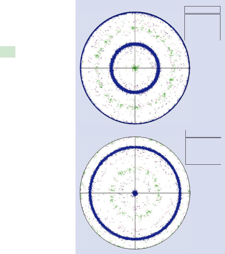
Pole figures are used to answer the question, Where does a particular crystallographic direction or plane fall in space relative to some arbitrary physical sample direction or plane? Pole figures have been used for many years and are very common in the preferred orientation or texture literature. In many cases a single pole figure does not provide sufficient information and additional pole figures of other crystallographic directions are required. A pole figure is simply a stereogram with the axes defined by the external reference frame. It is common for evaporated or deposited thin films to have a specific crystallographic direction parallel to the film growth direction. . Figure 29.17 is a series of pole figures from an evaporated Au thin film. In this example we show the [111] and the [110] pole figures. For the <111 > pole figure we note that there is a large number of poles plotted in the center of the pole figure. This shows that many of the pixels in the data set have the <111 > direction aligned with the sample normal. There are additional rings also in the <111 > pole figure. These are a result of there being more than one <111 > type direction in a cubic crystal (in fact there are actually four of these present). In the <110 > pole figure we see that there is a number of poles in the center of the pole figure indicating that there are a number of measured pixels with <110 > directions parallel to the sample normal direction.
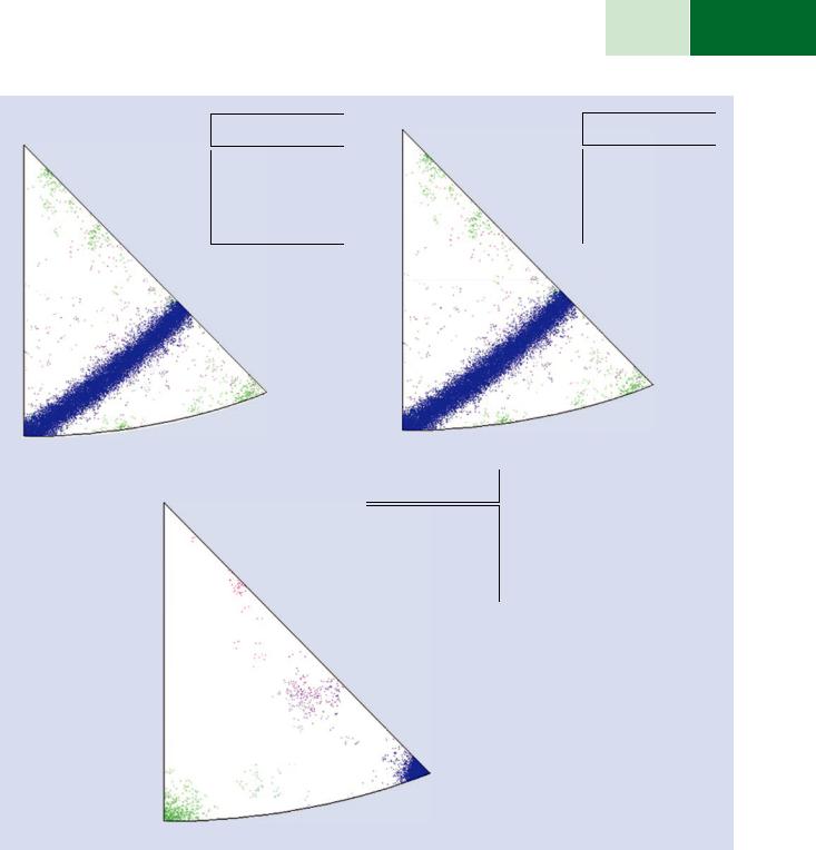
Inverse pole figures are used to answer the question, What crystallographic poles or planes are preferentially parallel or perpendicular to a specific sample direction? We usually again display these with respect to the physical axes of the microscope or the sample as described for the pole figures. For inverse pole figures we plot all of the directions that are pointing in a specific direction of the sample. Inverse pole figures are extremely useful for samples where there are specific axes of the sample that have a preferred crystallographic direction. . Figure 29.18 is an example of inverse pole figures plotted for the same Au-thin film shown in . Fig. 29.17. It is often helpful to show all three orthogonal directions so that the preferred texture can be visualized. Note that the inverse pole figures of . Fig. 29.18 show exactly the same information that is shown in . Fig. 29.17. It is sometimes helpful to first plot the inverse pole figures as they will give an indication of the samples texture without plotting pole figures of many different directions. The Z or surface normal direction of the inverse pole figures of . Fig. 29.18 is the one that carries the most information about the sample. Here we see the high density of pixel orientations that are clustered around the <111 > and less so around the <110 > directions.
Once we are familiar with the concepts of pole figures and inverse pole figures, we can then go ahead and understand inverse pole figure maps which are one of the more common ways that EBSD orientation data is shown. An inverse pole figure map extends the idea of an inverse pole
|
\506 |
Chapter 29 · Characterizing Crystalline Materials in the SEM |
|
|
|
. Fig. 29.17 Pole figures |
|
|
|
|
for an evaporated Au thin film |
|
|
|
|
constructed from EBSD data. In |
<110> |
Y0 |
|
|
the <110 > pole figure all of the |
|||
|
|
|||
|
|
|
||
|
<110 > directions are shown with |
|
|
|
|
respect to the growth direction. |
|
|
|
|
Note that there is some intensity |
|
|
|
|
in the center of the pole figure as |
|
|
|
|
a result of some of the grains hav- |
|
|
|
|
ing a <110 > pole parallel to the |
|
|
|
|
sample normal direction. In the |
|
|
|
|
<111 > pole figure note that there |
|
|
|
29 |
is large number of <111 > pole |
|
|
|
plotted in the center of the pole |
|
|
||
figure. This demonstrates that the majority of the grains have a <111 > direction parallel to the sample surface normal
<111> |
Y0 |
|
Pole figure
[Au_20kv_5kx_280pa_r: Iron fcc (m3m) Complete data set 39083 data points Equal Area projection Upper hemisphere
X0
Pole figure
[Au_20kv_5kx_280pa_r: Iron fcc (m3m) Complete data set 39083 data points Equal Area projection Upper hemisphere
X0
507 |
29 |
29.2 · Electron Backscatter Diffraction in the Scanning Electron Microscope
x0 |
Inverse Pole Figure |
001 |
x0 |
Inverse Pole Figure |
001 |
(Folded) |
|
|
(Folded) |
[Au_20kv_5kx_280pa_r: Iron fcc (m3m) Complete data set 39083 data points Equal Area projection Upper hermisphere
111 |
|
101 |
101 |
|
|
z0 |
Inverse Pole Figure |
001 |
(Folded) |
|
[Au_20kv_5kx_280pa_r: Iron fcc (m3m) Complete data set 39083 data points Equal Area projection Upper hermisphere
111
[Au_20kv_5kx_280pa_r: Iron fcc (m3m) Complete data set 39083 data points Equal Area projection Upper hermisphere
111
101
. Fig. 29.18 Inverse pole figures that show the same data as the pole figures in . Fig. 29.9. The three directions X, Y, and Z (parallel to the samples surface normal) are shown. The high density of poles plotted near the <111 > apex of the stereographic triangle indicates that many of the measured pixels had <111 > parallel to the sample surface normal
direction. The X and Y pole figures show where the other <111 > poles plot. The smaller density of poles near the <110 > apex of the triangle indicates that there are a few pixels with a <110 > direction parallel to the sample surface normal
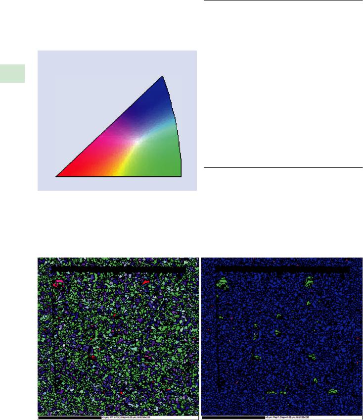
figure to an image. In order to do this we must first assign a color to each direction in the inverse pole figure stereographic triangle. A common way this is done is shown in
. Fig. 29.19. Inverse pole figure maps are then plotted by mapping the orientation of each pixel onto the color key shown in . Fig. 29.19. . Figure 29.20 is an inverse pole figure map produced from the same data that is shown as pole
figures (. Fig. 29.17) or inverse pole figures (. Fig. 29.18). When inverse pole figure maps are displayed it is important to always include the reference direction, otherwise it is difficult or impossible for the viewer to make sense of the information shown. . Figure 29.20 is an inverse pole figure map with respect to the surface normal direction or the Z direction. Thus, the map is mostly blue, indicating that most of the
\508 Chapter 29 · Characterizing Crystalline Materials in the SEM
grains have an <111 > direction normal to the sample surface. There are also some areas that are green in the map and these areas have an <110 > direction parallel to the surface normal. The inverse pole figure map with respect to the X direction looks totally different to the Z inverse pole figure map. Both of these are shown in . Fig. 29.20.
IPF colouring Iron fcc
29 |
Y0 |
111 |
|
||
|
|
29.2.7\ Other Map Components
Once the orientations of the pixels in an array are known, it is now possible to add additional information to the maps. There are many possible components the can be plotted based on EBSD data. One of the easiest components to add is that of grain boundaries. Grain boundaries are the planes (which intersect the planar surface as lines) that separate two regions of different crystallographic orientations. It is fairly trivial to calculate the change in orientations between two pixels. If we do this for an entire map we can then plot lines where the difference in orientations between two adjacent pixels exceeds a predefined limit. It is typically assumed that a grain boundary is represented by a change in orientation that exceeds 10°.
. Figure 29.20 has black lines plotted where the change in orientation exceeds this limit and thus the map shows the size of individual grains even though they are of consistent color due to the grain orientations with respect to the sample normal.
001 |
101 |
. Fig. 29.19 Typical color key used for inverse pole figure maps. This color key is used to color each pixel in an image to produce an inverse pole figure map or image. Thus, if a pixel has a <001 > direction parallel to a specific direction then we use this inverse pole figure key to plot that pixel as red. Or conversely, if we observe a red pixel in an orientation map we know the orientation of that pixel is close to <100 > parallel to the plotted direction
29.2.8\ Dangers and Practice of “Cleaning”
EBSD Data
Many of the currently available software platforms for EBSD allow users to modify the inverse pole figure maps in order to improve their appearance only (Brewer and Michael 2010). There are always pixels in a map that are either not indexed due to pattern quality or many other reasons or that are mis- indexed due to some sort of symmetry issues or multiple possible solutions to the bands that are found. These cleaning routines normally perform two separate operations. The first step is to remove the mis-indexed pixels. These pixels usually
. Fig. 29.20 Inverse pole figure maps from the X-direction (left) and the Z-direction (right). This is the same data that is shown in . Figs. 29.9 and 29.10. Inverse pole figure maps show the pixel-by-pixel or spatial arrangements of the crystal orientations (Bar = 5 µm)

509 |
29 |
29.2 · Electron Backscatter Diffraction in the Scanning Electron Microscope
show up as single pixels surrounded by correctly indexed pixels. The software searches through the data and where there is a single pixel of a different orientation surrounded by pixels of a different but similar orientation, the single mis-indexed pixel is replaced by the average of the surrounding orientations. The next step is to deal with the pixels that are not indexed. The same procedure is applied as with the single mis-indexed pixels in that kernel math is used. Each individual pixel has six nearest neighbors. If a cleaning procedure that requires six nearest neighbors to agree then the single un-indexed pixel is assigned the average orientation of it’s nearest neighbors. These procedures allow the user to select the number of nearest neighbors that must agree and using less than six nearest neighbors allows larger regions of pixels with no correct indexing to be replaced. Use of these procedures can be very dangerous and must be disclosed when inverse pole figure maps are published.
29.2.9\ Transmission Kikuchi Diffraction
in the SEM
One of the limitations of EBSD is that the resolution is compromised by the fact that the patterns are formed by backscattered electrons and that the sample is highly tilted leading to the previously mentioned fact that the resolution perpendicular to the tilt axis is much worse than that parallel to the tilt axis. The resolution can be greatly improved if the backscattered volume is reduced and the geometrical factors are reduced. One could image EBSD at reduced voltages to reduce the interaction volume, but this process has practical limitations related to the need for increased sample preparation quality. Also, improved EBSD cameras would be needed to take advantage of lower voltage operation. Lower voltage operation does nothing to reduce the geometrical effects.
Transmission Kikuchi diffraction (TKD, although some in the literature have referred to this method as t-EBSD, which is
the acronym for transmission electron backscattered diffraction, which is a rather non-physical description due to the inclusion of both transmission and backscattered in the name) is the transmission analog to EBSD is a way to achieve extremely high spatial resolution for crystallographic orientation or phase mapping (Keller and Geiss 2012; Trimby 2012). TKD is realized by using an electron-transparent sample, as in the transmission electron microscope, that is held at normal or nearnormal incidence with respect to the electron beam while a standard EBSD camera is placed at the exit surface of the sample, as shown in
. Fig. 29.21. Here the electron beam accelerating voltage must be high and the sample must be thin in order for transmission of the electrons to occur. The maximum beam energy typically available in modern SEMs is 30 kV, which requires that the sample must be quite thin. The use of a thin sample limits the size of the beam interaction volume within the sample and immediately improves the spatial resolution of TKD. In addition, the fact that the sample may be oriented normal to the incident electron beam further improves the resolution to the point that 2-nm spatial resolution has been achieved in TKD. It is incredibly fortuitous that the TKD patterns are extremely similar in appearance to EBSD patterns, as shown in . Fig. 29.22, and can be collected with the same cameras and the same analysis software as is used for EBSD. There are two main disadvantages to TKD. First, it may be difficult to produce appropriate thin samples. However, most laboratories will have access to a dual-plat- form FIB/SEM and thin samples prepared with FIB are perfectly adequate for TKD. The second disadvantage is that when a small pixel size is needed, it is difficult to map larger regions. For example, if a map step size of 4 nm is selected, a 1000 × 1000 pixel map will only cover 4× 4 μm. However, if orientation mapping of extremely fine grained material is needed, TKD may be the only way to achieve the resolution needed.
A typical TKD map acquired at 30 kV of a thinned sample of polycrystalline Si layers in a semiconductor device is shown in . Fig. 29.23. This map was acquired with a step size
a |
b |
. Fig. 29.21 Detector and sample positioning for transmission Kikuchi diffraction. a The detector shown is an on-axis detector. Sample and detector positioned and inserted for TKD with an on-axis
detector. Note row of solid state detectors located on the detector for collecting transmission images of the sample. b Sample and detector arrangement for TKD with a conventional style EBSD detector