

- •Preface
- •Imaging Microscopic Features
- •Measuring the Crystal Structure
- •References
- •Contents
- •1.4 Simulating the Effects of Elastic Scattering: Monte Carlo Calculations
- •What Are the Main Features of the Beam Electron Interaction Volume?
- •How Does the Interaction Volume Change with Composition?
- •How Does the Interaction Volume Change with Incident Beam Energy?
- •How Does the Interaction Volume Change with Specimen Tilt?
- •1.5 A Range Equation To Estimate the Size of the Interaction Volume
- •References
- •2: Backscattered Electrons
- •2.1 Origin
- •2.2.1 BSE Response to Specimen Composition (η vs. Atomic Number, Z)
- •SEM Image Contrast with BSE: “Atomic Number Contrast”
- •SEM Image Contrast: “BSE Topographic Contrast—Number Effects”
- •2.2.3 Angular Distribution of Backscattering
- •Beam Incident at an Acute Angle to the Specimen Surface (Specimen Tilt > 0°)
- •SEM Image Contrast: “BSE Topographic Contrast—Trajectory Effects”
- •2.2.4 Spatial Distribution of Backscattering
- •Depth Distribution of Backscattering
- •Radial Distribution of Backscattered Electrons
- •2.3 Summary
- •References
- •3: Secondary Electrons
- •3.1 Origin
- •3.2 Energy Distribution
- •3.3 Escape Depth of Secondary Electrons
- •3.8 Spatial Characteristics of Secondary Electrons
- •References
- •4: X-Rays
- •4.1 Overview
- •4.2 Characteristic X-Rays
- •4.2.1 Origin
- •4.2.2 Fluorescence Yield
- •4.2.3 X-Ray Families
- •4.2.4 X-Ray Nomenclature
- •4.2.6 Characteristic X-Ray Intensity
- •Isolated Atoms
- •X-Ray Production in Thin Foils
- •X-Ray Intensity Emitted from Thick, Solid Specimens
- •4.3 X-Ray Continuum (bremsstrahlung)
- •4.3.1 X-Ray Continuum Intensity
- •4.3.3 Range of X-ray Production
- •4.4 X-Ray Absorption
- •4.5 X-Ray Fluorescence
- •References
- •5.1 Electron Beam Parameters
- •5.2 Electron Optical Parameters
- •5.2.1 Beam Energy
- •Landing Energy
- •5.2.2 Beam Diameter
- •5.2.3 Beam Current
- •5.2.4 Beam Current Density
- •5.2.5 Beam Convergence Angle, α
- •5.2.6 Beam Solid Angle
- •5.2.7 Electron Optical Brightness, β
- •Brightness Equation
- •5.2.8 Focus
- •Astigmatism
- •5.3 SEM Imaging Modes
- •5.3.1 High Depth-of-Field Mode
- •5.3.2 High-Current Mode
- •5.3.3 Resolution Mode
- •5.3.4 Low-Voltage Mode
- •5.4 Electron Detectors
- •5.4.1 Important Properties of BSE and SE for Detector Design and Operation
- •Abundance
- •Angular Distribution
- •Kinetic Energy Response
- •5.4.2 Detector Characteristics
- •Angular Measures for Electron Detectors
- •Elevation (Take-Off) Angle, ψ, and Azimuthal Angle, ζ
- •Solid Angle, Ω
- •Energy Response
- •Bandwidth
- •5.4.3 Common Types of Electron Detectors
- •Backscattered Electrons
- •Passive Detectors
- •Scintillation Detectors
- •Semiconductor BSE Detectors
- •5.4.4 Secondary Electron Detectors
- •Everhart–Thornley Detector
- •Through-the-Lens (TTL) Electron Detectors
- •TTL SE Detector
- •TTL BSE Detector
- •Measuring the DQE: BSE Semiconductor Detector
- •References
- •6: Image Formation
- •6.1 Image Construction by Scanning Action
- •6.2 Magnification
- •6.3 Making Dimensional Measurements With the SEM: How Big Is That Feature?
- •Using a Calibrated Structure in ImageJ-Fiji
- •6.4 Image Defects
- •6.4.1 Projection Distortion (Foreshortening)
- •6.4.2 Image Defocusing (Blurring)
- •6.5 Making Measurements on Surfaces With Arbitrary Topography: Stereomicroscopy
- •6.5.1 Qualitative Stereomicroscopy
- •Fixed beam, Specimen Position Altered
- •Fixed Specimen, Beam Incidence Angle Changed
- •6.5.2 Quantitative Stereomicroscopy
- •Measuring a Simple Vertical Displacement
- •References
- •7: SEM Image Interpretation
- •7.1 Information in SEM Images
- •7.2.2 Calculating Atomic Number Contrast
- •Establishing a Robust Light-Optical Analogy
- •Getting It Wrong: Breaking the Light-Optical Analogy of the Everhart–Thornley (Positive Bias) Detector
- •Deconstructing the SEM/E–T Image of Topography
- •SUM Mode (A + B)
- •DIFFERENCE Mode (A−B)
- •References
- •References
- •9: Image Defects
- •9.1 Charging
- •9.1.1 What Is Specimen Charging?
- •9.1.3 Techniques to Control Charging Artifacts (High Vacuum Instruments)
- •Observing Uncoated Specimens
- •Coating an Insulating Specimen for Charge Dissipation
- •Choosing the Coating for Imaging Morphology
- •9.2 Radiation Damage
- •9.3 Contamination
- •References
- •10: High Resolution Imaging
- •10.2 Instrumentation Considerations
- •10.4.1 SE Range Effects Produce Bright Edges (Isolated Edges)
- •10.4.4 Too Much of a Good Thing: The Bright Edge Effect Hinders Locating the True Position of an Edge for Critical Dimension Metrology
- •10.5.1 Beam Energy Strategies
- •Low Beam Energy Strategy
- •High Beam Energy Strategy
- •Making More SE1: Apply a Thin High-δ Metal Coating
- •Making Fewer BSEs, SE2, and SE3 by Eliminating Bulk Scattering From the Substrate
- •10.6 Factors That Hinder Achieving High Resolution
- •10.6.2 Pathological Specimen Behavior
- •Contamination
- •Instabilities
- •References
- •11: Low Beam Energy SEM
- •11.3 Selecting the Beam Energy to Control the Spatial Sampling of Imaging Signals
- •11.3.1 Low Beam Energy for High Lateral Resolution SEM
- •11.3.2 Low Beam Energy for High Depth Resolution SEM
- •11.3.3 Extremely Low Beam Energy Imaging
- •References
- •12.1.1 Stable Electron Source Operation
- •12.1.2 Maintaining Beam Integrity
- •12.1.4 Minimizing Contamination
- •12.3.1 Control of Specimen Charging
- •12.5 VPSEM Image Resolution
- •References
- •13: ImageJ and Fiji
- •13.1 The ImageJ Universe
- •13.2 Fiji
- •13.3 Plugins
- •13.4 Where to Learn More
- •References
- •14: SEM Imaging Checklist
- •14.1.1 Conducting or Semiconducting Specimens
- •14.1.2 Insulating Specimens
- •14.2 Electron Signals Available
- •14.2.1 Beam Electron Range
- •14.2.2 Backscattered Electrons
- •14.2.3 Secondary Electrons
- •14.3 Selecting the Electron Detector
- •14.3.2 Backscattered Electron Detectors
- •14.3.3 “Through-the-Lens” Detectors
- •14.4 Selecting the Beam Energy for SEM Imaging
- •14.4.4 High Resolution SEM Imaging
- •Strategy 1
- •Strategy 2
- •14.5 Selecting the Beam Current
- •14.5.1 High Resolution Imaging
- •14.5.2 Low Contrast Features Require High Beam Current and/or Long Frame Time to Establish Visibility
- •14.6 Image Presentation
- •14.6.1 “Live” Display Adjustments
- •14.6.2 Post-Collection Processing
- •14.7 Image Interpretation
- •14.7.1 Observer’s Point of View
- •14.7.3 Contrast Encoding
- •14.8.1 VPSEM Advantages
- •14.8.2 VPSEM Disadvantages
- •15: SEM Case Studies
- •15.1 Case Study: How High Is That Feature Relative to Another?
- •15.2 Revealing Shallow Surface Relief
- •16.1.2 Minor Artifacts: The Si-Escape Peak
- •16.1.3 Minor Artifacts: Coincidence Peaks
- •16.1.4 Minor Artifacts: Si Absorption Edge and Si Internal Fluorescence Peak
- •16.2 “Best Practices” for Electron-Excited EDS Operation
- •16.2.1 Operation of the EDS System
- •Choosing the EDS Time Constant (Resolution and Throughput)
- •Choosing the Solid Angle of the EDS
- •Selecting a Beam Current for an Acceptable Level of System Dead-Time
- •16.3.1 Detector Geometry
- •16.3.2 Process Time
- •16.3.3 Optimal Working Distance
- •16.3.4 Detector Orientation
- •16.3.5 Count Rate Linearity
- •16.3.6 Energy Calibration Linearity
- •16.3.7 Other Items
- •16.3.8 Setting Up a Quality Control Program
- •Using the QC Tools Within DTSA-II
- •Creating a QC Project
- •Linearity of Output Count Rate with Live-Time Dose
- •Resolution and Peak Position Stability with Count Rate
- •Solid Angle for Low X-ray Flux
- •Maximizing Throughput at Moderate Resolution
- •References
- •17: DTSA-II EDS Software
- •17.1 Getting Started With NIST DTSA-II
- •17.1.1 Motivation
- •17.1.2 Platform
- •17.1.3 Overview
- •17.1.4 Design
- •Simulation
- •Quantification
- •Experiment Design
- •Modeled Detectors (. Fig. 17.1)
- •Window Type (. Fig. 17.2)
- •The Optimal Working Distance (. Figs. 17.3 and 17.4)
- •Elevation Angle
- •Sample-to-Detector Distance
- •Detector Area
- •Crystal Thickness
- •Number of Channels, Energy Scale, and Zero Offset
- •Resolution at Mn Kα (Approximate)
- •Azimuthal Angle
- •Gold Layer, Aluminum Layer, Nickel Layer
- •Dead Layer
- •Zero Strobe Discriminator (. Figs. 17.7 and 17.8)
- •Material Editor Dialog (. Figs. 17.9, 17.10, 17.11, 17.12, 17.13, and 17.14)
- •17.2.1 Introduction
- •17.2.2 Monte Carlo Simulation
- •17.2.4 Optional Tables
- •References
- •18: Qualitative Elemental Analysis by Energy Dispersive X-Ray Spectrometry
- •18.1 Quality Assurance Issues for Qualitative Analysis: EDS Calibration
- •18.2 Principles of Qualitative EDS Analysis
- •Exciting Characteristic X-Rays
- •Fluorescence Yield
- •X-ray Absorption
- •Si Escape Peak
- •Coincidence Peaks
- •18.3 Performing Manual Qualitative Analysis
- •Beam Energy
- •Choosing the EDS Resolution (Detector Time Constant)
- •Obtaining Adequate Counts
- •18.4.1 Employ the Available Software Tools
- •18.4.3 Lower Photon Energy Region
- •18.4.5 Checking Your Work
- •18.5 A Worked Example of Manual Peak Identification
- •References
- •19.1 What Is a k-ratio?
- •19.3 Sets of k-ratios
- •19.5 The Analytical Total
- •19.6 Normalization
- •19.7.1 Oxygen by Assumed Stoichiometry
- •19.7.3 Element by Difference
- •19.8 Ways of Reporting Composition
- •19.8.1 Mass Fraction
- •19.8.2 Atomic Fraction
- •19.8.3 Stoichiometry
- •19.8.4 Oxide Fractions
- •Example Calculations
- •19.9 The Accuracy of Quantitative Electron-Excited X-ray Microanalysis
- •19.9.1 Standards-Based k-ratio Protocol
- •19.9.2 “Standardless Analysis”
- •19.10 Appendix
- •19.10.1 The Need for Matrix Corrections To Achieve Quantitative Analysis
- •19.10.2 The Physical Origin of Matrix Effects
- •19.10.3 ZAF Factors in Microanalysis
- •X-ray Generation With Depth, φ(ρz)
- •X-ray Absorption Effect, A
- •X-ray Fluorescence, F
- •References
- •20.2 Instrumentation Requirements
- •20.2.1 Choosing the EDS Parameters
- •EDS Spectrum Channel Energy Width and Spectrum Energy Span
- •EDS Time Constant (Resolution and Throughput)
- •EDS Calibration
- •EDS Solid Angle
- •20.2.2 Choosing the Beam Energy, E0
- •20.2.3 Measuring the Beam Current
- •20.2.4 Choosing the Beam Current
- •Optimizing Analysis Strategy
- •20.3.4 Ba-Ti Interference in BaTiSi3O9
- •20.4 The Need for an Iterative Qualitative and Quantitative Analysis Strategy
- •20.4.2 Analysis of a Stainless Steel
- •20.5 Is the Specimen Homogeneous?
- •20.6 Beam-Sensitive Specimens
- •20.6.1 Alkali Element Migration
- •20.6.2 Materials Subject to Mass Loss During Electron Bombardment—the Marshall-Hall Method
- •Thin Section Analysis
- •Bulk Biological and Organic Specimens
- •References
- •21: Trace Analysis by SEM/EDS
- •21.1 Limits of Detection for SEM/EDS Microanalysis
- •21.2.1 Estimating CDL from a Trace or Minor Constituent from Measuring a Known Standard
- •21.2.2 Estimating CDL After Determination of a Minor or Trace Constituent with Severe Peak Interference from a Major Constituent
- •21.3 Measurements of Trace Constituents by Electron-Excited Energy Dispersive X-ray Spectrometry
- •The Inevitable Physics of Remote Excitation Within the Specimen: Secondary Fluorescence Beyond the Electron Interaction Volume
- •Simulation of Long-Range Secondary X-ray Fluorescence
- •NIST DTSA II Simulation: Vertical Interface Between Two Regions of Different Composition in a Flat Bulk Target
- •NIST DTSA II Simulation: Cubic Particle Embedded in a Bulk Matrix
- •21.5 Summary
- •References
- •22.1.2 Low Beam Energy Analysis Range
- •22.2 Advantage of Low Beam Energy X-Ray Microanalysis
- •22.2.1 Improved Spatial Resolution
- •22.3 Challenges and Limitations of Low Beam Energy X-Ray Microanalysis
- •22.3.1 Reduced Access to Elements
- •22.3.3 At Low Beam Energy, Almost Everything Is Found To Be Layered
- •Analysis of Surface Contamination
- •References
- •23: Analysis of Specimens with Special Geometry: Irregular Bulk Objects and Particles
- •23.2.1 No Chemical Etching
- •23.3 Consequences of Attempting Analysis of Bulk Materials With Rough Surfaces
- •23.4.1 The Raw Analytical Total
- •23.4.2 The Shape of the EDS Spectrum
- •23.5 Best Practices for Analysis of Rough Bulk Samples
- •23.6 Particle Analysis
- •Particle Sample Preparation: Bulk Substrate
- •The Importance of Beam Placement
- •Overscanning
- •“Particle Mass Effect”
- •“Particle Absorption Effect”
- •The Analytical Total Reveals the Impact of Particle Effects
- •Does Overscanning Help?
- •23.6.6 Peak-to-Background (P/B) Method
- •Specimen Geometry Severely Affects the k-ratio, but Not the P/B
- •Using the P/B Correspondence
- •23.7 Summary
- •References
- •24: Compositional Mapping
- •24.2 X-Ray Spectrum Imaging
- •24.2.1 Utilizing XSI Datacubes
- •24.2.2 Derived Spectra
- •SUM Spectrum
- •MAXIMUM PIXEL Spectrum
- •24.3 Quantitative Compositional Mapping
- •24.4 Strategy for XSI Elemental Mapping Data Collection
- •24.4.1 Choosing the EDS Dead-Time
- •24.4.2 Choosing the Pixel Density
- •24.4.3 Choosing the Pixel Dwell Time
- •“Flash Mapping”
- •High Count Mapping
- •References
- •25.1 Gas Scattering Effects in the VPSEM
- •25.1.1 Why Doesn’t the EDS Collimator Exclude the Remote Skirt X-Rays?
- •25.2 What Can Be Done To Minimize gas Scattering in VPSEM?
- •25.2.2 Favorable Sample Characteristics
- •Particle Analysis
- •25.2.3 Unfavorable Sample Characteristics
- •References
- •26.1 Instrumentation
- •26.1.2 EDS Detector
- •26.1.3 Probe Current Measurement Device
- •Direct Measurement: Using a Faraday Cup and Picoammeter
- •A Faraday Cup
- •Electrically Isolated Stage
- •Indirect Measurement: Using a Calibration Spectrum
- •26.1.4 Conductive Coating
- •26.2 Sample Preparation
- •26.2.1 Standard Materials
- •26.2.2 Peak Reference Materials
- •26.3 Initial Set-Up
- •26.3.1 Calibrating the EDS Detector
- •Selecting a Pulse Process Time Constant
- •Energy Calibration
- •Quality Control
- •Sample Orientation
- •Detector Position
- •Probe Current
- •26.4 Collecting Data
- •26.4.1 Exploratory Spectrum
- •26.4.2 Experiment Optimization
- •26.4.3 Selecting Standards
- •26.4.4 Reference Spectra
- •26.4.5 Collecting Standards
- •26.4.6 Collecting Peak-Fitting References
- •26.5 Data Analysis
- •26.5.2 Quantification
- •26.6 Quality Check
- •Reference
- •27.2 Case Study: Aluminum Wire Failures in Residential Wiring
- •References
- •28: Cathodoluminescence
- •28.1 Origin
- •28.2 Measuring Cathodoluminescence
- •28.3 Applications of CL
- •28.3.1 Geology
- •Carbonado Diamond
- •Ancient Impact Zircons
- •28.3.2 Materials Science
- •Semiconductors
- •Lead-Acid Battery Plate Reactions
- •28.3.3 Organic Compounds
- •References
- •29.1.1 Single Crystals
- •29.1.2 Polycrystalline Materials
- •29.1.3 Conditions for Detecting Electron Channeling Contrast
- •Specimen Preparation
- •Instrument Conditions
- •29.2.1 Origin of EBSD Patterns
- •29.2.2 Cameras for EBSD Pattern Detection
- •29.2.3 EBSD Spatial Resolution
- •29.2.5 Steps in Typical EBSD Measurements
- •Sample Preparation for EBSD
- •Align Sample in the SEM
- •Check for EBSD Patterns
- •Adjust SEM and Select EBSD Map Parameters
- •Run the Automated Map
- •29.2.6 Display of the Acquired Data
- •29.2.7 Other Map Components
- •29.2.10 Application Example
- •Application of EBSD To Understand Meteorite Formation
- •29.2.11 Summary
- •Specimen Considerations
- •EBSD Detector
- •Selection of Candidate Crystallographic Phases
- •Microscope Operating Conditions and Pattern Optimization
- •Selection of EBSD Acquisition Parameters
- •Collect the Orientation Map
- •References
- •30.1 Introduction
- •30.2 Ion–Solid Interactions
- •30.3 Focused Ion Beam Systems
- •30.5 Preparation of Samples for SEM
- •30.5.1 Cross-Section Preparation
- •30.5.2 FIB Sample Preparation for 3D Techniques and Imaging
- •30.6 Summary
- •References
- •31: Ion Beam Microscopy
- •31.1 What Is So Useful About Ions?
- •31.2 Generating Ion Beams
- •31.3 Signal Generation in the HIM
- •31.5 Patterning with Ion Beams
- •31.7 Chemical Microanalysis with Ion Beams
- •References
- •Appendix
- •A Database of Electron–Solid Interactions
- •A Database of Electron–Solid Interactions
- •Introduction
- •Backscattered Electrons
- •Secondary Yields
- •Stopping Powers
- •X-ray Ionization Cross Sections
- •Conclusions
- •References
- •Index
- •Reference List
- •Index
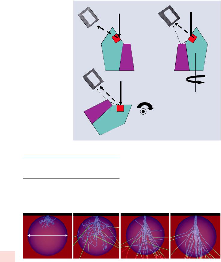
394\ Chapter 23 · Analysis of Specimens with Special Geometry: Irregular Bulk Objects and Particles
. Fig. 23.16 Schematic illustration of orientation movements to optimize EDS collection from a feature of a rough, irregular surface: a initial position gives high absorption due to X-ray path through bulk of specimen; b rotation about a vertical axis brings feature to directly face EDS; c rotation about a horizontal axis places feature perpendicular to beam to minimize backscattering and remote X-ray excitation
b
EDS |
EDS |
|
Better!
Bad!
c
EDS
23.6\ Particle Analysis
23.6.1\ How Do X-ray Measurements
of Particles Differ From Bulk
Measurements?
The analysis of microscopic particles whose dimensions approach or are smaller than the interaction volume in a bulk target of the same composition is subject to effects similar to analyzing rough, bulk surfaces but with additional challenges. Like the rough bulk case, the curved or locally
Best, but still compromised!
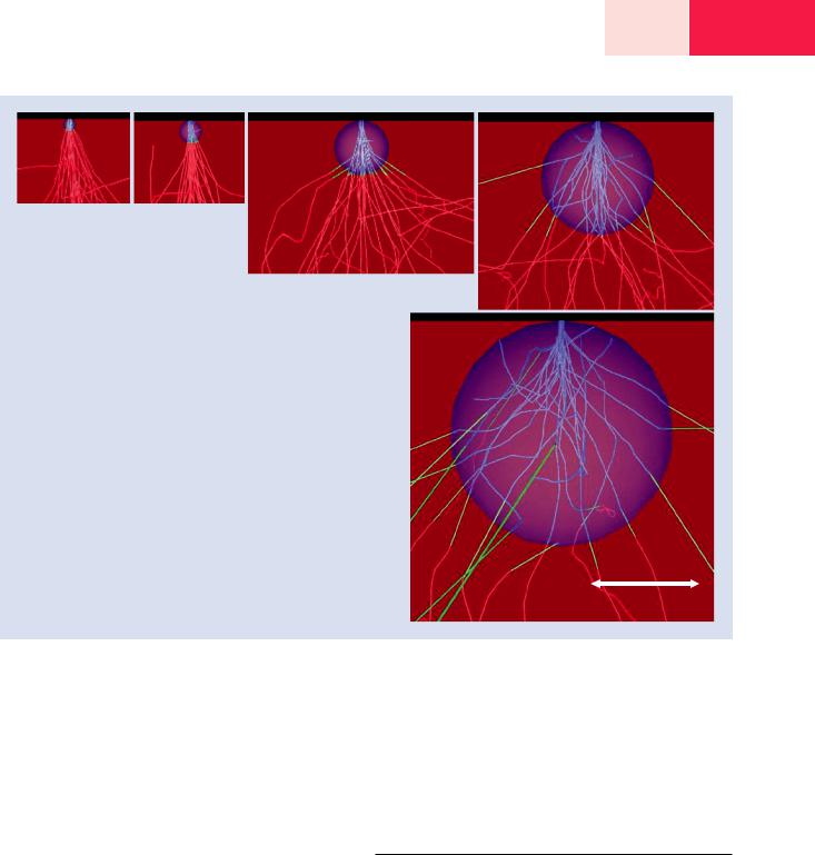
tilted surface of a particle acts to modify electron backscattering, which alters X-ray production, while deviations from the ideal flat surface alter the X-ray path to the detector, which modifies X-ray absorption compared to a flat bulk target. The geometry of a particle leads to additional loss of beam electrons due to penetration through the sides and bottom of the particle, as shown in the DTSA-II Monte Carlo simulations in . Fig. 23.17, which depict trajectories in a 1 μm-diameter aluminum particle at different beam energies. At the highest energy simulated, E0 = 30 keV, most trajectories pass through the particle with some lateral
5 keV |
10 keV |
20 keV |
30 keV |
1µm Al
23
. Fig. 23.17 DTSA-II Monte Carlo simulation of electron trajectories in a 1-μm-diameter Al sphere on a bulk C substrate at various beam energies; incident beam diameter = 50 nm. Trajectories inside the Al
particle are blue. Green shows trajectories that emerge from the Al particle which change to orange when they enter the C substrate
395 |
23 |
23.6 · Particle Analysis
0.1 µm |
0.2 µm |
0.5 µm
1 µm
Al spheres on bulk C
E0 = 20 keV
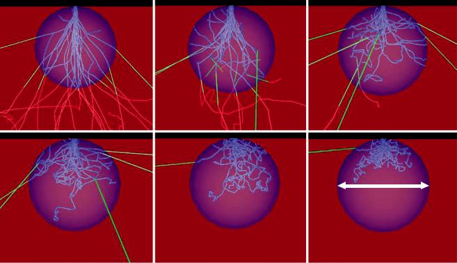
2 µm |
1 µm |
. Fig. 23.18 DTSA-II Monte Carlo simulation of electron trajectories in Al spheres of various diameters at E0 = 20 keV on a bulk C substrate. Trajectories inside the Al particle are blue. Green shows trajectories that
emerge from the Al particle which change to orange when they enter the C substrate
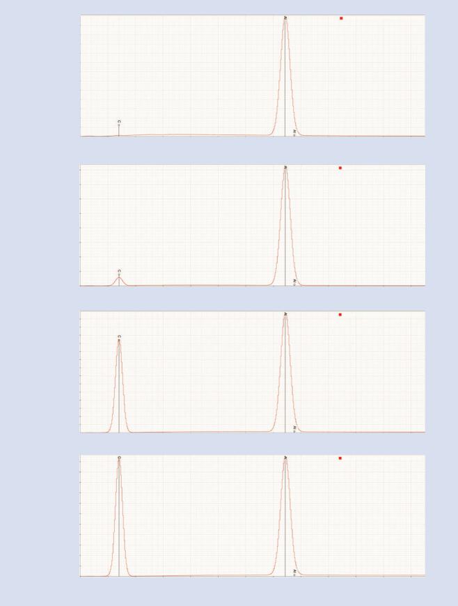
scattering. As the beam energy is lowered and the electron range decreases, penetration through the bottom and sides diminishes, and at E0 = 5 keV the interaction volume is completely contained within the 1-μm-diameter aluminum particle. The beam penetration effect also depends on the particle size, as shown in . Fig. 23.18 for particles of various sizes at E0 = 20 keV, and on composition, as shown for particles with a range of atomic numbers in . Fig. 23.19. Moreover, as opposed to the backscattered electrons in the high angle portion of the cosine distribution which are likely to leave the vicinity of the particle without further interaction, the beam electrons that penetrate through the sides and bottom of the particle are likely to reach the supporting substrate where they will create X-rays of the substrate material that contribute to the overall spectrum measured. This effect can be seen in . Fig. 23.20, which shows the Al and C peaks calculated by the Monte Carlo simulation for 1-μm diameter Al spherical particles. At a beam energy of E0 = 5 keV, the electron trajectories are contained within the particle which effectively acts like a bulk target. No electrons penetrate the sides or bottom to reach the substrate so there is no C contribution to the EDS spectrum. With increasing incident
energy, electron penetration through the particle into the substrate occurs, and the C peak of the substrate increases relative to the Al-peak from the particle.
23.6.2\ Collecting Optimum Spectra
From Particles
Before meaningful qualitative and quantitative analysis of particles can be attempted, it is important to optimize the EDS spectrum that is collected. As illustrated in the trajectory plots in the Monte Carlo simulations shown in
. Figs. 23.17, 23.18, and 23.19, and the calculated spectra shown in 23.20, because of the impact of particle size and shape (geometry) on electron interactions, the EDS spectrum of a particle will always be compromised compared to the spectrum of a material of identical composition in the ideal flat, bulk form. The analyst must be aware of the major factors that modify particle spectra and seek to minimize these effects. The particle spectrum can be optimized through careful sample preparation and by understanding of the factors that affect the strategy for beam placement.
396\ Chapter 23 · Analysis of Specimens with Special Geometry: Irregular Bulk Objects and Particles
Al |
Ti |
Cu |
|
Ag |
Hf |
Au |
1 µm
. Fig. 23.19 DTSA-II Monte Carlo simulation of electron trajectories at E0 = 20 keV in 1 μm-diameter spheres of various elements (Al, Ti, Cu, Ag, Hf, Au) on a bulk C substrate. Trajectories inside the particles are
blue. Green shows trajectories that emerge from the particle which change to orange when they enter the C substrate
Particle Sample Preparation: Bulk Substrate
|
Because beam electrons can penetrate through the sides and |
|
bottom of a particle and reach the underlying substrate, the |
|
measured spectrum will always be a composite of contribu- |
|
tions from the particle and the substrate, as shown in |
|
. Fig. 23.21 for a K411 glass particle (~1 μm in diameter) on |
|
a bulk carbon substrate. To obtain a spectrum that is repre- |
|
sentative of the particle material alone, it is important when- |
|
ever possible to choose a substrate consisting of an element(s) |
|
not contained in the particle of interest. As part of a quality |
|
measurement system, the EDS spectrum of the blank sub- |
|
strate material should be measured to determine what ele- |
|
ments are present at the major, minor, and trace level. |
|
Additionally, it is desirable that the characteristic peak(s) of |
|
the substrate element(s) should not interfere with character- |
|
istic peaks from the constituents of the particle. |
|
Carbon is an excellent choice for a bulk substrate since it is |
|
available in high purity, is mechanically robust, and supplied |
|
by various vendors as planchets with different surface finishes, |
|
including a highly polished, glassy surface that is nearly fea- |
|
tureless as a background for SEM imaging of small particles. |
|
The low energy of the C K X-ray (0.285 keV) is unlikely to |
|
cause interference with most elements of interest. In addition |
|
|
23 |
to bulk substrates, carbon is often used in the form of carbon- |
|
infused tape with a sticky surface to which particles will read- |
ily adhere. If a carbon tape preparation is used, the analyst
must measure a blank spectrum of the tape since the polymer base of the tape frequently contains elements such as oxygen in addition to carbon. If carbon is of analytical interest, other low atomic number substrates are available, including high purity boron and beryllium (but beware of the health hazard of handling beryllium, especially in the form of beryllium oxide which may be released by surface abrasion). Other pure element substrates such as aluminum and silicon can be used if that element(s) is not of interest, but because of the high
degree of excitation of the Al K-L2,3 and Si K-L2,3 characteristic X-rays under typical operating conditions, a significant
fraction of the EDS deadtime will be taken up by the substrate X-rays, diminishing the analytical information collected per unit time on the particle of interest, as well as contributing coincidence peaks that might be misinterpreted as minor or trace constituents, for example, 2 Al K-L2,3 (2.974 keV) is close
to the energy of Ag L3-M4,5 (2.981 keV) and 2 Si K-L2,3 (3.480 keV) is close to the energy of Sn L3-M4,5 (3.440 keV)
When depositing particles on a substrate, the area density should be minimized to avoid situations where electrons scattered off the particle being analyzed can strike nearby particles and excite X-rays, which will then contribute an artifact (“cross talk”). While this remote excitation is likely to be at the equivalent of a minor or trace level constituent, it is critical to understand such contributions when low level constituents are of interest.
23.6 · Particle Analysis
a130000
120000
110000
100000
|
90000 |
|
|
Intensity counts |
80000 |
|
|
70000 |
|
|
|
|
|
|
|
|
60000 |
|
|
|
50000 |
|
|
|
40000 |
|
|
|
30000 |
|
|
|
20000 |
|
|
|
10000 |
|
|
|
0 |
0 |
|
b |
400000 |
|
|
|
|
||
|
350000 |
|
|
|
300000 |
|
|
Intensity counts |
250000 |
|
|
200000 |
|
|
|
|
|
|
|
|
150000 |
|
|
|
100000 |
|
|
|
50000 |
|
|
|
0 |
|
|
|
0 |
||
c |
280000 |
|
|
|
|
||
|
|
|
|
|
260000 |
|
|
|
240000 |
|
|
|
220000 |
|
|
|
220000 |
|
|
|
|
|
|
Intensity counts |
180000 |
|
|
120000 |
|
|
|
|
160000 |
|
|
|
140000 |
|
|
|
100000 |
|
|
|
80000 |
|
|
|
60000 |
|
|
|
40000 |
|
|
|
20000 |
|
|
|
0 |
|
|
|
0 |
||
d |
220000 |
|
|
|
|
||
|
|
|
|
|
200000 |
|
|
|
180000 |
|
|
|
160000 |
|
|
Intensity counts |
140000 |
|
|
120000 |
|
|
|
|
|
|
|
|
100000 |
|
|
|
80000 |
|
|
|
60000 |
|
|
|
40000 |
|
|
|
20000 |
|
|
|
0 |
|
|
|
0 |
||
397 |
|
23 |
|
|
|
E0 = 5 keV |
Noisy[MC simulation of a 1.000 mm |
diameter sphere of Al on] 5keV |
200 400 600 800 1000 1200 1400 1600 1700 2000 2200 2400 Photon energy (eV)
|
Noisy[MC simulation of a 1.000 mm |
E0 = 10 keV |
diameter sphere of Al on C] 10keV |
|
200 400 600 800 1000 1200 1400 1600 1800 2000 2200 2400 Photon energy (eV)
E0 |
= 20 keV |
Noisy[MC simulation of a 1.000 mm |
|
diameter sphere of Al on C] 20keV |
|||
|
|
200 |
400 |
600 |
800 |
1000 |
1200 |
1400 |
1600 |
1800 |
2000 |
2200 |
2400 |
|
|
|
|
Photon energy (eV) |
|
|
|
|
|
||
Noisy[MC simulation of a 1.000 mm
diameter sphere of Al on C] 30keV
E0 = 30 keV
200 |
400 |
600 |
700 |
1000 |
1200 |
1400 |
1600 |
1800 |
2000 |
2200 |
2400 |
|
|
|
|
Photon energy (eV) |
|
|
|
|
|
||
. Fig. 23.20 EDS spectra calculated with the DTSA-II Monte Carlo simulation for a 1-μm-diameter Al particle on a C substrate at various beam energies: a 5 keV, b 10 keV, c 20 keV, and d 30 keV. Note the
absence of the C peak from the substrate at E0 = 5 keV, its appearance at E0 = 10 keV and the increase relative to the Al peak as the beam energy increases
\398 Chapter 23 · Analysis of Specimens with Special Geometry: Irregular Bulk Objects and Particles
K411_sphere-on-tape_20kV10nA
K411_sphere-on-film_20kV10nA
Counts
0.0 |
1.0 |
2.0 |
3.0 |
4.0 |
5.0 |
6.0 |
7.0 |
8.0 |
9.0 |
10.0 |
Photon energy (keV)
Counts
K411_sphere-on-tape_20kV10nA
K411_sphere-on-film_20kV10nA
K411
E0 = 20 keV
C – tape substrate
C film (20 nm) on Cu grid
0.0 |
1.0 |
2.0 |
3.0 |
4.0 |
5.0 |
6.0 |
7.0 |
8.0 |
9.0 |
10.0 |
|
|
|
|
|
Photon energy (keV) |
|
|
|
|
|
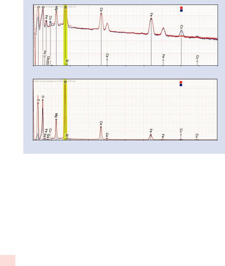
. Fig. 23.21 Comparison of EDS spectra similar sized K411 spheres mounted on a bulk carbon substrate (red) and on a 20-nm-thick carbon film on a copper support grid blue). Note artifact Cu peaks arising from lateral electron scattering from particle to excite the support grid
Particle Sample Preparation: Minimizing
Substrate Contributions With a Thin Foil Substrate
As the particle dimensions decrease below 1 μm, electron penetration through the particle increases dramatically, raising the substrate contribution to the X-ray spectrum. Even if the characteristic peak(s) of the substrate material is not of interest and can be ignored, the deadtime due to the substrate spectrum will eventually dominate the overall spectrum measurement, even if the substrate consists of carbon which is relatively poorly excited. Moreover, the contribution of the substrate to the composite spectrum occurs not only from the characteristic peak(s), for example, C K, but also from the continuum background (bremsstrahlung) which affects all photon energies. Increased background from the substrate has the effect of lowering the peak-to-background for all characteristic peaks from the elements of the particle, which
23 degrades all aspects of quantitative analysis but especially impacts the limit of detection, raising the minimum concentration that can be reliably measured.
The substrate contribution to the composite spectrum can be minimized by reducing the mass of the substrate. Fine particles, especially those with nanometer dimensions, can be dispersed by various methods, including air-jetting or deposition from fluid drops, onto thin carbon films, typically 20 nm in thickness, which are supported on a grid (copper, nickel, carbon, etc.), as shown in the sequence of images in . Fig. 23.22. To further stabilize the particle deposit, it is typical practice to apply a thin (<10 nm) carbon coating to provide conductivity and also to provide some mechanical constraint. The contribution to the spectrum from the thin carbon support film plus the final coating is much reduced compared to the situation on a bulk or thick tape carbon substrate, as shown in the comparison of spectra from K411 particles of similar size (~1 μm in diameter) shown in . Fig. 23.21. Beam electrons that are scattered laterally from particles can excite the material of the grid, as shown by the presence of copper in the K411 particle spectrum of . Fig. 23.21, but if this system radiation is problematic, this unwanted spectral contribution can be controlled by choosing alternative grid materials, such as carbon.