

- •Preface
- •Imaging Microscopic Features
- •Measuring the Crystal Structure
- •References
- •Contents
- •1.4 Simulating the Effects of Elastic Scattering: Monte Carlo Calculations
- •What Are the Main Features of the Beam Electron Interaction Volume?
- •How Does the Interaction Volume Change with Composition?
- •How Does the Interaction Volume Change with Incident Beam Energy?
- •How Does the Interaction Volume Change with Specimen Tilt?
- •1.5 A Range Equation To Estimate the Size of the Interaction Volume
- •References
- •2: Backscattered Electrons
- •2.1 Origin
- •2.2.1 BSE Response to Specimen Composition (η vs. Atomic Number, Z)
- •SEM Image Contrast with BSE: “Atomic Number Contrast”
- •SEM Image Contrast: “BSE Topographic Contrast—Number Effects”
- •2.2.3 Angular Distribution of Backscattering
- •Beam Incident at an Acute Angle to the Specimen Surface (Specimen Tilt > 0°)
- •SEM Image Contrast: “BSE Topographic Contrast—Trajectory Effects”
- •2.2.4 Spatial Distribution of Backscattering
- •Depth Distribution of Backscattering
- •Radial Distribution of Backscattered Electrons
- •2.3 Summary
- •References
- •3: Secondary Electrons
- •3.1 Origin
- •3.2 Energy Distribution
- •3.3 Escape Depth of Secondary Electrons
- •3.8 Spatial Characteristics of Secondary Electrons
- •References
- •4: X-Rays
- •4.1 Overview
- •4.2 Characteristic X-Rays
- •4.2.1 Origin
- •4.2.2 Fluorescence Yield
- •4.2.3 X-Ray Families
- •4.2.4 X-Ray Nomenclature
- •4.2.6 Characteristic X-Ray Intensity
- •Isolated Atoms
- •X-Ray Production in Thin Foils
- •X-Ray Intensity Emitted from Thick, Solid Specimens
- •4.3 X-Ray Continuum (bremsstrahlung)
- •4.3.1 X-Ray Continuum Intensity
- •4.3.3 Range of X-ray Production
- •4.4 X-Ray Absorption
- •4.5 X-Ray Fluorescence
- •References
- •5.1 Electron Beam Parameters
- •5.2 Electron Optical Parameters
- •5.2.1 Beam Energy
- •Landing Energy
- •5.2.2 Beam Diameter
- •5.2.3 Beam Current
- •5.2.4 Beam Current Density
- •5.2.5 Beam Convergence Angle, α
- •5.2.6 Beam Solid Angle
- •5.2.7 Electron Optical Brightness, β
- •Brightness Equation
- •5.2.8 Focus
- •Astigmatism
- •5.3 SEM Imaging Modes
- •5.3.1 High Depth-of-Field Mode
- •5.3.2 High-Current Mode
- •5.3.3 Resolution Mode
- •5.3.4 Low-Voltage Mode
- •5.4 Electron Detectors
- •5.4.1 Important Properties of BSE and SE for Detector Design and Operation
- •Abundance
- •Angular Distribution
- •Kinetic Energy Response
- •5.4.2 Detector Characteristics
- •Angular Measures for Electron Detectors
- •Elevation (Take-Off) Angle, ψ, and Azimuthal Angle, ζ
- •Solid Angle, Ω
- •Energy Response
- •Bandwidth
- •5.4.3 Common Types of Electron Detectors
- •Backscattered Electrons
- •Passive Detectors
- •Scintillation Detectors
- •Semiconductor BSE Detectors
- •5.4.4 Secondary Electron Detectors
- •Everhart–Thornley Detector
- •Through-the-Lens (TTL) Electron Detectors
- •TTL SE Detector
- •TTL BSE Detector
- •Measuring the DQE: BSE Semiconductor Detector
- •References
- •6: Image Formation
- •6.1 Image Construction by Scanning Action
- •6.2 Magnification
- •6.3 Making Dimensional Measurements With the SEM: How Big Is That Feature?
- •Using a Calibrated Structure in ImageJ-Fiji
- •6.4 Image Defects
- •6.4.1 Projection Distortion (Foreshortening)
- •6.4.2 Image Defocusing (Blurring)
- •6.5 Making Measurements on Surfaces With Arbitrary Topography: Stereomicroscopy
- •6.5.1 Qualitative Stereomicroscopy
- •Fixed beam, Specimen Position Altered
- •Fixed Specimen, Beam Incidence Angle Changed
- •6.5.2 Quantitative Stereomicroscopy
- •Measuring a Simple Vertical Displacement
- •References
- •7: SEM Image Interpretation
- •7.1 Information in SEM Images
- •7.2.2 Calculating Atomic Number Contrast
- •Establishing a Robust Light-Optical Analogy
- •Getting It Wrong: Breaking the Light-Optical Analogy of the Everhart–Thornley (Positive Bias) Detector
- •Deconstructing the SEM/E–T Image of Topography
- •SUM Mode (A + B)
- •DIFFERENCE Mode (A−B)
- •References
- •References
- •9: Image Defects
- •9.1 Charging
- •9.1.1 What Is Specimen Charging?
- •9.1.3 Techniques to Control Charging Artifacts (High Vacuum Instruments)
- •Observing Uncoated Specimens
- •Coating an Insulating Specimen for Charge Dissipation
- •Choosing the Coating for Imaging Morphology
- •9.2 Radiation Damage
- •9.3 Contamination
- •References
- •10: High Resolution Imaging
- •10.2 Instrumentation Considerations
- •10.4.1 SE Range Effects Produce Bright Edges (Isolated Edges)
- •10.4.4 Too Much of a Good Thing: The Bright Edge Effect Hinders Locating the True Position of an Edge for Critical Dimension Metrology
- •10.5.1 Beam Energy Strategies
- •Low Beam Energy Strategy
- •High Beam Energy Strategy
- •Making More SE1: Apply a Thin High-δ Metal Coating
- •Making Fewer BSEs, SE2, and SE3 by Eliminating Bulk Scattering From the Substrate
- •10.6 Factors That Hinder Achieving High Resolution
- •10.6.2 Pathological Specimen Behavior
- •Contamination
- •Instabilities
- •References
- •11: Low Beam Energy SEM
- •11.3 Selecting the Beam Energy to Control the Spatial Sampling of Imaging Signals
- •11.3.1 Low Beam Energy for High Lateral Resolution SEM
- •11.3.2 Low Beam Energy for High Depth Resolution SEM
- •11.3.3 Extremely Low Beam Energy Imaging
- •References
- •12.1.1 Stable Electron Source Operation
- •12.1.2 Maintaining Beam Integrity
- •12.1.4 Minimizing Contamination
- •12.3.1 Control of Specimen Charging
- •12.5 VPSEM Image Resolution
- •References
- •13: ImageJ and Fiji
- •13.1 The ImageJ Universe
- •13.2 Fiji
- •13.3 Plugins
- •13.4 Where to Learn More
- •References
- •14: SEM Imaging Checklist
- •14.1.1 Conducting or Semiconducting Specimens
- •14.1.2 Insulating Specimens
- •14.2 Electron Signals Available
- •14.2.1 Beam Electron Range
- •14.2.2 Backscattered Electrons
- •14.2.3 Secondary Electrons
- •14.3 Selecting the Electron Detector
- •14.3.2 Backscattered Electron Detectors
- •14.3.3 “Through-the-Lens” Detectors
- •14.4 Selecting the Beam Energy for SEM Imaging
- •14.4.4 High Resolution SEM Imaging
- •Strategy 1
- •Strategy 2
- •14.5 Selecting the Beam Current
- •14.5.1 High Resolution Imaging
- •14.5.2 Low Contrast Features Require High Beam Current and/or Long Frame Time to Establish Visibility
- •14.6 Image Presentation
- •14.6.1 “Live” Display Adjustments
- •14.6.2 Post-Collection Processing
- •14.7 Image Interpretation
- •14.7.1 Observer’s Point of View
- •14.7.3 Contrast Encoding
- •14.8.1 VPSEM Advantages
- •14.8.2 VPSEM Disadvantages
- •15: SEM Case Studies
- •15.1 Case Study: How High Is That Feature Relative to Another?
- •15.2 Revealing Shallow Surface Relief
- •16.1.2 Minor Artifacts: The Si-Escape Peak
- •16.1.3 Minor Artifacts: Coincidence Peaks
- •16.1.4 Minor Artifacts: Si Absorption Edge and Si Internal Fluorescence Peak
- •16.2 “Best Practices” for Electron-Excited EDS Operation
- •16.2.1 Operation of the EDS System
- •Choosing the EDS Time Constant (Resolution and Throughput)
- •Choosing the Solid Angle of the EDS
- •Selecting a Beam Current for an Acceptable Level of System Dead-Time
- •16.3.1 Detector Geometry
- •16.3.2 Process Time
- •16.3.3 Optimal Working Distance
- •16.3.4 Detector Orientation
- •16.3.5 Count Rate Linearity
- •16.3.6 Energy Calibration Linearity
- •16.3.7 Other Items
- •16.3.8 Setting Up a Quality Control Program
- •Using the QC Tools Within DTSA-II
- •Creating a QC Project
- •Linearity of Output Count Rate with Live-Time Dose
- •Resolution and Peak Position Stability with Count Rate
- •Solid Angle for Low X-ray Flux
- •Maximizing Throughput at Moderate Resolution
- •References
- •17: DTSA-II EDS Software
- •17.1 Getting Started With NIST DTSA-II
- •17.1.1 Motivation
- •17.1.2 Platform
- •17.1.3 Overview
- •17.1.4 Design
- •Simulation
- •Quantification
- •Experiment Design
- •Modeled Detectors (. Fig. 17.1)
- •Window Type (. Fig. 17.2)
- •The Optimal Working Distance (. Figs. 17.3 and 17.4)
- •Elevation Angle
- •Sample-to-Detector Distance
- •Detector Area
- •Crystal Thickness
- •Number of Channels, Energy Scale, and Zero Offset
- •Resolution at Mn Kα (Approximate)
- •Azimuthal Angle
- •Gold Layer, Aluminum Layer, Nickel Layer
- •Dead Layer
- •Zero Strobe Discriminator (. Figs. 17.7 and 17.8)
- •Material Editor Dialog (. Figs. 17.9, 17.10, 17.11, 17.12, 17.13, and 17.14)
- •17.2.1 Introduction
- •17.2.2 Monte Carlo Simulation
- •17.2.4 Optional Tables
- •References
- •18: Qualitative Elemental Analysis by Energy Dispersive X-Ray Spectrometry
- •18.1 Quality Assurance Issues for Qualitative Analysis: EDS Calibration
- •18.2 Principles of Qualitative EDS Analysis
- •Exciting Characteristic X-Rays
- •Fluorescence Yield
- •X-ray Absorption
- •Si Escape Peak
- •Coincidence Peaks
- •18.3 Performing Manual Qualitative Analysis
- •Beam Energy
- •Choosing the EDS Resolution (Detector Time Constant)
- •Obtaining Adequate Counts
- •18.4.1 Employ the Available Software Tools
- •18.4.3 Lower Photon Energy Region
- •18.4.5 Checking Your Work
- •18.5 A Worked Example of Manual Peak Identification
- •References
- •19.1 What Is a k-ratio?
- •19.3 Sets of k-ratios
- •19.5 The Analytical Total
- •19.6 Normalization
- •19.7.1 Oxygen by Assumed Stoichiometry
- •19.7.3 Element by Difference
- •19.8 Ways of Reporting Composition
- •19.8.1 Mass Fraction
- •19.8.2 Atomic Fraction
- •19.8.3 Stoichiometry
- •19.8.4 Oxide Fractions
- •Example Calculations
- •19.9 The Accuracy of Quantitative Electron-Excited X-ray Microanalysis
- •19.9.1 Standards-Based k-ratio Protocol
- •19.9.2 “Standardless Analysis”
- •19.10 Appendix
- •19.10.1 The Need for Matrix Corrections To Achieve Quantitative Analysis
- •19.10.2 The Physical Origin of Matrix Effects
- •19.10.3 ZAF Factors in Microanalysis
- •X-ray Generation With Depth, φ(ρz)
- •X-ray Absorption Effect, A
- •X-ray Fluorescence, F
- •References
- •20.2 Instrumentation Requirements
- •20.2.1 Choosing the EDS Parameters
- •EDS Spectrum Channel Energy Width and Spectrum Energy Span
- •EDS Time Constant (Resolution and Throughput)
- •EDS Calibration
- •EDS Solid Angle
- •20.2.2 Choosing the Beam Energy, E0
- •20.2.3 Measuring the Beam Current
- •20.2.4 Choosing the Beam Current
- •Optimizing Analysis Strategy
- •20.3.4 Ba-Ti Interference in BaTiSi3O9
- •20.4 The Need for an Iterative Qualitative and Quantitative Analysis Strategy
- •20.4.2 Analysis of a Stainless Steel
- •20.5 Is the Specimen Homogeneous?
- •20.6 Beam-Sensitive Specimens
- •20.6.1 Alkali Element Migration
- •20.6.2 Materials Subject to Mass Loss During Electron Bombardment—the Marshall-Hall Method
- •Thin Section Analysis
- •Bulk Biological and Organic Specimens
- •References
- •21: Trace Analysis by SEM/EDS
- •21.1 Limits of Detection for SEM/EDS Microanalysis
- •21.2.1 Estimating CDL from a Trace or Minor Constituent from Measuring a Known Standard
- •21.2.2 Estimating CDL After Determination of a Minor or Trace Constituent with Severe Peak Interference from a Major Constituent
- •21.3 Measurements of Trace Constituents by Electron-Excited Energy Dispersive X-ray Spectrometry
- •The Inevitable Physics of Remote Excitation Within the Specimen: Secondary Fluorescence Beyond the Electron Interaction Volume
- •Simulation of Long-Range Secondary X-ray Fluorescence
- •NIST DTSA II Simulation: Vertical Interface Between Two Regions of Different Composition in a Flat Bulk Target
- •NIST DTSA II Simulation: Cubic Particle Embedded in a Bulk Matrix
- •21.5 Summary
- •References
- •22.1.2 Low Beam Energy Analysis Range
- •22.2 Advantage of Low Beam Energy X-Ray Microanalysis
- •22.2.1 Improved Spatial Resolution
- •22.3 Challenges and Limitations of Low Beam Energy X-Ray Microanalysis
- •22.3.1 Reduced Access to Elements
- •22.3.3 At Low Beam Energy, Almost Everything Is Found To Be Layered
- •Analysis of Surface Contamination
- •References
- •23: Analysis of Specimens with Special Geometry: Irregular Bulk Objects and Particles
- •23.2.1 No Chemical Etching
- •23.3 Consequences of Attempting Analysis of Bulk Materials With Rough Surfaces
- •23.4.1 The Raw Analytical Total
- •23.4.2 The Shape of the EDS Spectrum
- •23.5 Best Practices for Analysis of Rough Bulk Samples
- •23.6 Particle Analysis
- •Particle Sample Preparation: Bulk Substrate
- •The Importance of Beam Placement
- •Overscanning
- •“Particle Mass Effect”
- •“Particle Absorption Effect”
- •The Analytical Total Reveals the Impact of Particle Effects
- •Does Overscanning Help?
- •23.6.6 Peak-to-Background (P/B) Method
- •Specimen Geometry Severely Affects the k-ratio, but Not the P/B
- •Using the P/B Correspondence
- •23.7 Summary
- •References
- •24: Compositional Mapping
- •24.2 X-Ray Spectrum Imaging
- •24.2.1 Utilizing XSI Datacubes
- •24.2.2 Derived Spectra
- •SUM Spectrum
- •MAXIMUM PIXEL Spectrum
- •24.3 Quantitative Compositional Mapping
- •24.4 Strategy for XSI Elemental Mapping Data Collection
- •24.4.1 Choosing the EDS Dead-Time
- •24.4.2 Choosing the Pixel Density
- •24.4.3 Choosing the Pixel Dwell Time
- •“Flash Mapping”
- •High Count Mapping
- •References
- •25.1 Gas Scattering Effects in the VPSEM
- •25.1.1 Why Doesn’t the EDS Collimator Exclude the Remote Skirt X-Rays?
- •25.2 What Can Be Done To Minimize gas Scattering in VPSEM?
- •25.2.2 Favorable Sample Characteristics
- •Particle Analysis
- •25.2.3 Unfavorable Sample Characteristics
- •References
- •26.1 Instrumentation
- •26.1.2 EDS Detector
- •26.1.3 Probe Current Measurement Device
- •Direct Measurement: Using a Faraday Cup and Picoammeter
- •A Faraday Cup
- •Electrically Isolated Stage
- •Indirect Measurement: Using a Calibration Spectrum
- •26.1.4 Conductive Coating
- •26.2 Sample Preparation
- •26.2.1 Standard Materials
- •26.2.2 Peak Reference Materials
- •26.3 Initial Set-Up
- •26.3.1 Calibrating the EDS Detector
- •Selecting a Pulse Process Time Constant
- •Energy Calibration
- •Quality Control
- •Sample Orientation
- •Detector Position
- •Probe Current
- •26.4 Collecting Data
- •26.4.1 Exploratory Spectrum
- •26.4.2 Experiment Optimization
- •26.4.3 Selecting Standards
- •26.4.4 Reference Spectra
- •26.4.5 Collecting Standards
- •26.4.6 Collecting Peak-Fitting References
- •26.5 Data Analysis
- •26.5.2 Quantification
- •26.6 Quality Check
- •Reference
- •27.2 Case Study: Aluminum Wire Failures in Residential Wiring
- •References
- •28: Cathodoluminescence
- •28.1 Origin
- •28.2 Measuring Cathodoluminescence
- •28.3 Applications of CL
- •28.3.1 Geology
- •Carbonado Diamond
- •Ancient Impact Zircons
- •28.3.2 Materials Science
- •Semiconductors
- •Lead-Acid Battery Plate Reactions
- •28.3.3 Organic Compounds
- •References
- •29.1.1 Single Crystals
- •29.1.2 Polycrystalline Materials
- •29.1.3 Conditions for Detecting Electron Channeling Contrast
- •Specimen Preparation
- •Instrument Conditions
- •29.2.1 Origin of EBSD Patterns
- •29.2.2 Cameras for EBSD Pattern Detection
- •29.2.3 EBSD Spatial Resolution
- •29.2.5 Steps in Typical EBSD Measurements
- •Sample Preparation for EBSD
- •Align Sample in the SEM
- •Check for EBSD Patterns
- •Adjust SEM and Select EBSD Map Parameters
- •Run the Automated Map
- •29.2.6 Display of the Acquired Data
- •29.2.7 Other Map Components
- •29.2.10 Application Example
- •Application of EBSD To Understand Meteorite Formation
- •29.2.11 Summary
- •Specimen Considerations
- •EBSD Detector
- •Selection of Candidate Crystallographic Phases
- •Microscope Operating Conditions and Pattern Optimization
- •Selection of EBSD Acquisition Parameters
- •Collect the Orientation Map
- •References
- •30.1 Introduction
- •30.2 Ion–Solid Interactions
- •30.3 Focused Ion Beam Systems
- •30.5 Preparation of Samples for SEM
- •30.5.1 Cross-Section Preparation
- •30.5.2 FIB Sample Preparation for 3D Techniques and Imaging
- •30.6 Summary
- •References
- •31: Ion Beam Microscopy
- •31.1 What Is So Useful About Ions?
- •31.2 Generating Ion Beams
- •31.3 Signal Generation in the HIM
- •31.5 Patterning with Ion Beams
- •31.7 Chemical Microanalysis with Ion Beams
- •References
- •Appendix
- •A Database of Electron–Solid Interactions
- •A Database of Electron–Solid Interactions
- •Introduction
- •Backscattered Electrons
- •Secondary Yields
- •Stopping Powers
- •X-ray Ionization Cross Sections
- •Conclusions
- •References
- •Index
- •Reference List
- •Index
9.1 · Charging
magnification image of a large plastic sphere (5 mm in diameter) that was first subjected to bombardment at E0 = 10 keV, followed by imaging at E0 = 2 keV where the deposited charge acts to reflect the beam and produce a “fish-eye” lens view of the SEM chamber. Close examination of the higher magnification PSL images shows that each of these microscopic spheres is acting like a tiny “fish-eye lens” and producing a highly distorted view of the SEM chamber.
9.1.3\ Techniques to Control Charging Artifacts (High Vacuum Instruments)
Observing Uncoated Specimens
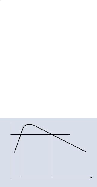
To understand the basic charging behavior of an uncoated insulator imaged with different selections of the incident beam energy, consider . Fig. 9.9, which shows the behavior of the processes of backscattering and secondary electron emission as a function of beam energy. For beam energies above 5 keV, generally η + δ < 1, so that more electrons are injected into the specimen by the beam than leave as BSEs and SEs, leading to an accumulation of negative charge in an insulator. For most materials, especially insulators, as the beam energy is lowered, the total emission of BSEs and SEs increases, eventually reaching an upper cross-over energy, E2 (which typically lies in the range 2–5 keV depending on the material) where η + δ = 1, and the charge injected by the beam is just balanced by the charge leaving as BSEs and SEs. If a beam energy is selected just above E2 where η + δ < 1, the local buildup of negative charge acts to repel the subsequent incoming beam electrons while the beam remains at that pixel, lowering the effective kinetic energy with which the beam strikes the surface eventually reaching the E2 energy and a dynamically stable charge balance. For beam energies below the E2 value and above the lower cross-over energy E1 (approximately
1.0 |
|
|
η+δ |
|
|
~ 0.5-1 keV |
~ 2-5 keV |
|
E1 |
E2 |
E0 |
. Fig. 9.9 Schematic illustration of the total emission of backscattered electrons and secondary electrons as a function of incident beam energy; note upper and lower cross-over energies where η + δ = 1
139 |
|
9 |
|
|
|
0.5–2 keV, depending on the material), the emission of SE can actually reach very large values for insulators with δmax ranging from 2 to 20 depending on the material. Thus, in this beam energy region η + δ > 1, resulting in positive charging which increases the kinetic energy of the incoming beam electrons until the E2 energy is reached and charge balance occurs. This dynamic charge stability enables uncoated insulators to be imaged, as shown in the example of the uncoated mineral particle shown in . Fig. 9.10, where a charge-free image is obtained at E0 = 1 keV, but charging effects are observed at E0 ≥2 keV. Achieving effective “dynamic charge balance microscopy” is sensitive to material and specimen shape (local tilt as it affects BSEs and particularly SE emission), and success depends on optimizing several instrument parameters: beam energy, beam current, and scan speed. Note that the uncoated mineral specimen used in the beam energy sequence in . Fig. 9.10 is the same used for the pixel dwell time sequence at E0 = 1 keV in . Fig. 9.6 where charging is observed when longer dwell times are used, demonstrating the complex response of charging to multiple variables.
Coating an Insulating Specimen for Charge Dissipation
Conductive coatings can be deposited by thermal evaporation with electron beam heating (metals, alloys) or with resistive heating (carbon), by high energy ion beam sputtering (metals, alloys), or by low energy plasma ion sputtering (alloys). The coating must cover all of the specimen, including complex topographic shapes, to provide a continuous conducting path across the surface to dissipate the charge injected into the specimen by the electron beam. It is important to coat all surfaces that are directly exposed to the electron beam or which might receive charge from BSEs, possibly after rescattering of those BSEs. Note that applying a conductive coating alone may not be sufficient to achieve efficient charge dissipation. Many specimens may be so thick that the sides may not actually receive an adequate amount of the coating material, as illustrated in . Fig. 9.11, even with rotation during the coating process. It is necessary to complete the path from the coating to the electrical ground with a conducting material that exhibits a low vapor pressure material that is compatible with the microscope’s vacuum requirement, such as a metal wire, conducting tape, or metal foil.
It is desirable to make the coating as thin as possible, and for many samples an effective conducting film can be 2–10 nm in thickness. A beam with E0 > 5 keV will penetrate through this coating and 10–100 times (or more) deeper depending on material and the incident beam energy, thus depositing most of the charge in the insulator itself. However, the presence of a ground plane and conducting path nanometers to micrometers away from the implanted charge creates a very high local field gradient, >106 V/m, apparently leading to continuous breakdown and discharging. The strongest evidence that a continuous discharge situation is established
\140 Chapter 9 · Image Defects
1 keV |
|
2 keV |
|
|
|
5 keV |
|
10 keV |
|
|
|
9
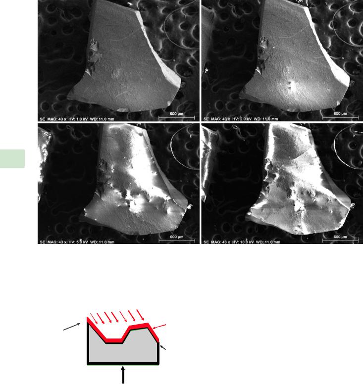
. Fig. 9.10 Beam energy sequence showing development of charging as the energy is increased. Specimen: uncoated quartz fragment; 1.6 μs per pixel dwell time; Everhart–Thornley (positive bias) detector
|
|
Directional coating source |
||
|
|
|
|
Coating |
|
|
|
|
|
Grounding |
|
|
|
|
connection |
|
|
|
|
from coating |
|
|
Bare, |
|
to ground |
|
|
||
|
|
insulating |
||
(e.g., |
|
|
||
|
|
surface |
||
conducting |
|
|
||
|
|
Rotate specimen |
||
tape, wire) |
|
|
||
|
|
|
|
during coating |
|
|
|
|
|
|
|
|
|
|
. Fig. 9.11 Schematic diagram showing the need to provide a grounding path from a surface coating due to uncoated or poorly coated sides of a non-conducting specimen
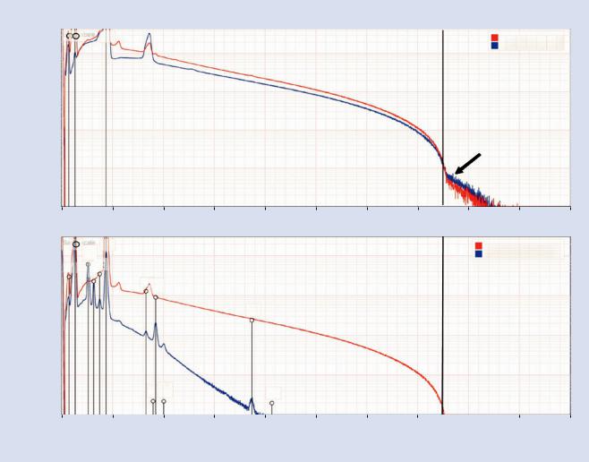
that avoids the build-up of charge is the behavior of the Duane–Hunt energy limit of the X-ray continuum. As the beam electrons are decelerated in the Coulombic field of the atoms, the energy lost is emitted as photons of electromagnetic radiation, termed bremsstrahlung, or braking radiation, and forming a continuous spectrum of photon energies up to the incident beam energy, which is the Duane–Hunt energy limit. Examination of the upper limit with a calibrated EDS detector provides proof of the highest energy with which beam electrons enter the specimen. When charging occurs, the potential that is developed serves to decelerate subsequent beam electrons and reduce the effective E0 with which they arrive, lowering the Duane–Hunt energy limit. . Figure 9.12 illustrates such an experiment. The true beam energy should first be confirmed by measuring the Duane–Hunt limit with a conducting high atomic number metal such as tantalum or gold, which produces a high continuum intensity since Icm
9.1 · Charging
|
|
|
|
Si |
|
100000 |
|
|
|
|
10000 |
|
|
|
Counts |
1000 |
|
|
|
|
|
|
|
|
|
100 |
|
|
|
|
10 |
0 |
|
2 |
1000000 |
|
Na |
Si |
|
|
|
AI |
||
|
|
|
|
|
|
|
C |
Mg |
|
|
100000 |
|
|
|
Counts |
10000 |
|
|
|
|
|
|
|
|
|
1000 |
|
|
|
|
10 |
|
|
|
|
|
0 |
|
2 |
NIST DTSA II Duane Hunt fitted value: |
|
|||
SiO2 (C, 8 nm) |
|
15.08 keV |
|
|
Si |
|
15.11 keV |
|
|
4 |
6 |
8 |
10 |
12 |
|
|
|
Photon Energy (keV) |
|
|
NIST DTSA II Duane Hunt fitted value: |
|
||
|
SiO2 (C, 8 nm) |
15.08 keV |
|
|
Ca K |
Glass (Uncoated) |
8 keV |
|
|
|
|
|
|
|
|
|
Ni |
|
|
Ca K |
|
|
Ni |
|
4 |
6 |
8 |
10 |
12 |
|
|
|
Photon Energy (keV) |
|
141 |
|
9 |
|
|
|
15keV
SiO2_15keV20nA_4ks
Si_15keV20nA_2ks
Coincidence counts
14 |
16 |
18 |
20 |
15 keV
SiO2_15keV20nA_4ks
BareGlass_15keV20nA_2ks
14 |
16 |
18 |
20 |
. Fig. 9.12 Effects of charging on the Duane–Hunt energy limit of the X-ray continuum: (upper) comparison of silicon and coated (C, 8 nm) SiO2 showing almost identical values; (lower) comparison of
coated (C, 8 nm) SiO2 and uncoated glass showing significant depression of the Duane–Hunt limit due to charging
scales with the atomic number. Note that because of pulse coincidence events, there will always be a small number of photons measured above the true Duane–Hunt limit. The true limit can be estimated with good accuracy by fitting the upper energy range of the continuum intensity, preferably over a region that is several kilo-electronvolts in width and that does not contain any characteristic X-ray peaks, and then finding where the curve intersects zero intensity to define the Duane–Hunt limit. NIST DTSA II performs such a fit and the result is recorded in the metadata reported for each spectrum processed. Once the beam energy is established on a conducting specimen, then the experiment consists of measuring a coated and uncoated insulator. In
. Fig. 9.12 (upper plot) spectra are shown for Si (measured Duane–Hunt limit = 15.11 keV) and coated (C, 8 nm) SiO2 (measured Duane–Hunt limit = 15.08 keV), which indicates
there is no significant charging in the coated SiO2. When an uncoated glass slide is bombarded at E0 = 15 keV, the charging induced by the electron beam causes charging and thus severely depresses the Duane–Hunt limit to 8 keV, as seen in
. Fig. 9.12 (lower plot), as well as a sharp difference in the shape of the X-ray continuum at higher photon energy.
Choosing the Coating for Imaging Morphology
The ideal coating should be continuous and featureless so that it does not interfere with imaging the true fine-scale features of the specimen. Since the SE1 signal is such an important source of high resolution information, a material that has a high SE coefficient should be chosen. Because the SE1 signal originates within a thin surface layer that is a few nanometers in thickness, having this layer consist of a high atomic number material such as gold that has a high SE