
- •Preface
- •Imaging Microscopic Features
- •Measuring the Crystal Structure
- •References
- •Contents
- •1.4 Simulating the Effects of Elastic Scattering: Monte Carlo Calculations
- •What Are the Main Features of the Beam Electron Interaction Volume?
- •How Does the Interaction Volume Change with Composition?
- •How Does the Interaction Volume Change with Incident Beam Energy?
- •How Does the Interaction Volume Change with Specimen Tilt?
- •1.5 A Range Equation To Estimate the Size of the Interaction Volume
- •References
- •2: Backscattered Electrons
- •2.1 Origin
- •2.2.1 BSE Response to Specimen Composition (η vs. Atomic Number, Z)
- •SEM Image Contrast with BSE: “Atomic Number Contrast”
- •SEM Image Contrast: “BSE Topographic Contrast—Number Effects”
- •2.2.3 Angular Distribution of Backscattering
- •Beam Incident at an Acute Angle to the Specimen Surface (Specimen Tilt > 0°)
- •SEM Image Contrast: “BSE Topographic Contrast—Trajectory Effects”
- •2.2.4 Spatial Distribution of Backscattering
- •Depth Distribution of Backscattering
- •Radial Distribution of Backscattered Electrons
- •2.3 Summary
- •References
- •3: Secondary Electrons
- •3.1 Origin
- •3.2 Energy Distribution
- •3.3 Escape Depth of Secondary Electrons
- •3.8 Spatial Characteristics of Secondary Electrons
- •References
- •4: X-Rays
- •4.1 Overview
- •4.2 Characteristic X-Rays
- •4.2.1 Origin
- •4.2.2 Fluorescence Yield
- •4.2.3 X-Ray Families
- •4.2.4 X-Ray Nomenclature
- •4.2.6 Characteristic X-Ray Intensity
- •Isolated Atoms
- •X-Ray Production in Thin Foils
- •X-Ray Intensity Emitted from Thick, Solid Specimens
- •4.3 X-Ray Continuum (bremsstrahlung)
- •4.3.1 X-Ray Continuum Intensity
- •4.3.3 Range of X-ray Production
- •4.4 X-Ray Absorption
- •4.5 X-Ray Fluorescence
- •References
- •5.1 Electron Beam Parameters
- •5.2 Electron Optical Parameters
- •5.2.1 Beam Energy
- •Landing Energy
- •5.2.2 Beam Diameter
- •5.2.3 Beam Current
- •5.2.4 Beam Current Density
- •5.2.5 Beam Convergence Angle, α
- •5.2.6 Beam Solid Angle
- •5.2.7 Electron Optical Brightness, β
- •Brightness Equation
- •5.2.8 Focus
- •Astigmatism
- •5.3 SEM Imaging Modes
- •5.3.1 High Depth-of-Field Mode
- •5.3.2 High-Current Mode
- •5.3.3 Resolution Mode
- •5.3.4 Low-Voltage Mode
- •5.4 Electron Detectors
- •5.4.1 Important Properties of BSE and SE for Detector Design and Operation
- •Abundance
- •Angular Distribution
- •Kinetic Energy Response
- •5.4.2 Detector Characteristics
- •Angular Measures for Electron Detectors
- •Elevation (Take-Off) Angle, ψ, and Azimuthal Angle, ζ
- •Solid Angle, Ω
- •Energy Response
- •Bandwidth
- •5.4.3 Common Types of Electron Detectors
- •Backscattered Electrons
- •Passive Detectors
- •Scintillation Detectors
- •Semiconductor BSE Detectors
- •5.4.4 Secondary Electron Detectors
- •Everhart–Thornley Detector
- •Through-the-Lens (TTL) Electron Detectors
- •TTL SE Detector
- •TTL BSE Detector
- •Measuring the DQE: BSE Semiconductor Detector
- •References
- •6: Image Formation
- •6.1 Image Construction by Scanning Action
- •6.2 Magnification
- •6.3 Making Dimensional Measurements With the SEM: How Big Is That Feature?
- •Using a Calibrated Structure in ImageJ-Fiji
- •6.4 Image Defects
- •6.4.1 Projection Distortion (Foreshortening)
- •6.4.2 Image Defocusing (Blurring)
- •6.5 Making Measurements on Surfaces With Arbitrary Topography: Stereomicroscopy
- •6.5.1 Qualitative Stereomicroscopy
- •Fixed beam, Specimen Position Altered
- •Fixed Specimen, Beam Incidence Angle Changed
- •6.5.2 Quantitative Stereomicroscopy
- •Measuring a Simple Vertical Displacement
- •References
- •7: SEM Image Interpretation
- •7.1 Information in SEM Images
- •7.2.2 Calculating Atomic Number Contrast
- •Establishing a Robust Light-Optical Analogy
- •Getting It Wrong: Breaking the Light-Optical Analogy of the Everhart–Thornley (Positive Bias) Detector
- •Deconstructing the SEM/E–T Image of Topography
- •SUM Mode (A + B)
- •DIFFERENCE Mode (A−B)
- •References
- •References
- •9: Image Defects
- •9.1 Charging
- •9.1.1 What Is Specimen Charging?
- •9.1.3 Techniques to Control Charging Artifacts (High Vacuum Instruments)
- •Observing Uncoated Specimens
- •Coating an Insulating Specimen for Charge Dissipation
- •Choosing the Coating for Imaging Morphology
- •9.2 Radiation Damage
- •9.3 Contamination
- •References
- •10: High Resolution Imaging
- •10.2 Instrumentation Considerations
- •10.4.1 SE Range Effects Produce Bright Edges (Isolated Edges)
- •10.4.4 Too Much of a Good Thing: The Bright Edge Effect Hinders Locating the True Position of an Edge for Critical Dimension Metrology
- •10.5.1 Beam Energy Strategies
- •Low Beam Energy Strategy
- •High Beam Energy Strategy
- •Making More SE1: Apply a Thin High-δ Metal Coating
- •Making Fewer BSEs, SE2, and SE3 by Eliminating Bulk Scattering From the Substrate
- •10.6 Factors That Hinder Achieving High Resolution
- •10.6.2 Pathological Specimen Behavior
- •Contamination
- •Instabilities
- •References
- •11: Low Beam Energy SEM
- •11.3 Selecting the Beam Energy to Control the Spatial Sampling of Imaging Signals
- •11.3.1 Low Beam Energy for High Lateral Resolution SEM
- •11.3.2 Low Beam Energy for High Depth Resolution SEM
- •11.3.3 Extremely Low Beam Energy Imaging
- •References
- •12.1.1 Stable Electron Source Operation
- •12.1.2 Maintaining Beam Integrity
- •12.1.4 Minimizing Contamination
- •12.3.1 Control of Specimen Charging
- •12.5 VPSEM Image Resolution
- •References
- •13: ImageJ and Fiji
- •13.1 The ImageJ Universe
- •13.2 Fiji
- •13.3 Plugins
- •13.4 Where to Learn More
- •References
- •14: SEM Imaging Checklist
- •14.1.1 Conducting or Semiconducting Specimens
- •14.1.2 Insulating Specimens
- •14.2 Electron Signals Available
- •14.2.1 Beam Electron Range
- •14.2.2 Backscattered Electrons
- •14.2.3 Secondary Electrons
- •14.3 Selecting the Electron Detector
- •14.3.2 Backscattered Electron Detectors
- •14.3.3 “Through-the-Lens” Detectors
- •14.4 Selecting the Beam Energy for SEM Imaging
- •14.4.4 High Resolution SEM Imaging
- •Strategy 1
- •Strategy 2
- •14.5 Selecting the Beam Current
- •14.5.1 High Resolution Imaging
- •14.5.2 Low Contrast Features Require High Beam Current and/or Long Frame Time to Establish Visibility
- •14.6 Image Presentation
- •14.6.1 “Live” Display Adjustments
- •14.6.2 Post-Collection Processing
- •14.7 Image Interpretation
- •14.7.1 Observer’s Point of View
- •14.7.3 Contrast Encoding
- •14.8.1 VPSEM Advantages
- •14.8.2 VPSEM Disadvantages
- •15: SEM Case Studies
- •15.1 Case Study: How High Is That Feature Relative to Another?
- •15.2 Revealing Shallow Surface Relief
- •16.1.2 Minor Artifacts: The Si-Escape Peak
- •16.1.3 Minor Artifacts: Coincidence Peaks
- •16.1.4 Minor Artifacts: Si Absorption Edge and Si Internal Fluorescence Peak
- •16.2 “Best Practices” for Electron-Excited EDS Operation
- •16.2.1 Operation of the EDS System
- •Choosing the EDS Time Constant (Resolution and Throughput)
- •Choosing the Solid Angle of the EDS
- •Selecting a Beam Current for an Acceptable Level of System Dead-Time
- •16.3.1 Detector Geometry
- •16.3.2 Process Time
- •16.3.3 Optimal Working Distance
- •16.3.4 Detector Orientation
- •16.3.5 Count Rate Linearity
- •16.3.6 Energy Calibration Linearity
- •16.3.7 Other Items
- •16.3.8 Setting Up a Quality Control Program
- •Using the QC Tools Within DTSA-II
- •Creating a QC Project
- •Linearity of Output Count Rate with Live-Time Dose
- •Resolution and Peak Position Stability with Count Rate
- •Solid Angle for Low X-ray Flux
- •Maximizing Throughput at Moderate Resolution
- •References
- •17: DTSA-II EDS Software
- •17.1 Getting Started With NIST DTSA-II
- •17.1.1 Motivation
- •17.1.2 Platform
- •17.1.3 Overview
- •17.1.4 Design
- •Simulation
- •Quantification
- •Experiment Design
- •Modeled Detectors (. Fig. 17.1)
- •Window Type (. Fig. 17.2)
- •The Optimal Working Distance (. Figs. 17.3 and 17.4)
- •Elevation Angle
- •Sample-to-Detector Distance
- •Detector Area
- •Crystal Thickness
- •Number of Channels, Energy Scale, and Zero Offset
- •Resolution at Mn Kα (Approximate)
- •Azimuthal Angle
- •Gold Layer, Aluminum Layer, Nickel Layer
- •Dead Layer
- •Zero Strobe Discriminator (. Figs. 17.7 and 17.8)
- •Material Editor Dialog (. Figs. 17.9, 17.10, 17.11, 17.12, 17.13, and 17.14)
- •17.2.1 Introduction
- •17.2.2 Monte Carlo Simulation
- •17.2.4 Optional Tables
- •References
- •18: Qualitative Elemental Analysis by Energy Dispersive X-Ray Spectrometry
- •18.1 Quality Assurance Issues for Qualitative Analysis: EDS Calibration
- •18.2 Principles of Qualitative EDS Analysis
- •Exciting Characteristic X-Rays
- •Fluorescence Yield
- •X-ray Absorption
- •Si Escape Peak
- •Coincidence Peaks
- •18.3 Performing Manual Qualitative Analysis
- •Beam Energy
- •Choosing the EDS Resolution (Detector Time Constant)
- •Obtaining Adequate Counts
- •18.4.1 Employ the Available Software Tools
- •18.4.3 Lower Photon Energy Region
- •18.4.5 Checking Your Work
- •18.5 A Worked Example of Manual Peak Identification
- •References
- •19.1 What Is a k-ratio?
- •19.3 Sets of k-ratios
- •19.5 The Analytical Total
- •19.6 Normalization
- •19.7.1 Oxygen by Assumed Stoichiometry
- •19.7.3 Element by Difference
- •19.8 Ways of Reporting Composition
- •19.8.1 Mass Fraction
- •19.8.2 Atomic Fraction
- •19.8.3 Stoichiometry
- •19.8.4 Oxide Fractions
- •Example Calculations
- •19.9 The Accuracy of Quantitative Electron-Excited X-ray Microanalysis
- •19.9.1 Standards-Based k-ratio Protocol
- •19.9.2 “Standardless Analysis”
- •19.10 Appendix
- •19.10.1 The Need for Matrix Corrections To Achieve Quantitative Analysis
- •19.10.2 The Physical Origin of Matrix Effects
- •19.10.3 ZAF Factors in Microanalysis
- •X-ray Generation With Depth, φ(ρz)
- •X-ray Absorption Effect, A
- •X-ray Fluorescence, F
- •References
- •20.2 Instrumentation Requirements
- •20.2.1 Choosing the EDS Parameters
- •EDS Spectrum Channel Energy Width and Spectrum Energy Span
- •EDS Time Constant (Resolution and Throughput)
- •EDS Calibration
- •EDS Solid Angle
- •20.2.2 Choosing the Beam Energy, E0
- •20.2.3 Measuring the Beam Current
- •20.2.4 Choosing the Beam Current
- •Optimizing Analysis Strategy
- •20.3.4 Ba-Ti Interference in BaTiSi3O9
- •20.4 The Need for an Iterative Qualitative and Quantitative Analysis Strategy
- •20.4.2 Analysis of a Stainless Steel
- •20.5 Is the Specimen Homogeneous?
- •20.6 Beam-Sensitive Specimens
- •20.6.1 Alkali Element Migration
- •20.6.2 Materials Subject to Mass Loss During Electron Bombardment—the Marshall-Hall Method
- •Thin Section Analysis
- •Bulk Biological and Organic Specimens
- •References
- •21: Trace Analysis by SEM/EDS
- •21.1 Limits of Detection for SEM/EDS Microanalysis
- •21.2.1 Estimating CDL from a Trace or Minor Constituent from Measuring a Known Standard
- •21.2.2 Estimating CDL After Determination of a Minor or Trace Constituent with Severe Peak Interference from a Major Constituent
- •21.3 Measurements of Trace Constituents by Electron-Excited Energy Dispersive X-ray Spectrometry
- •The Inevitable Physics of Remote Excitation Within the Specimen: Secondary Fluorescence Beyond the Electron Interaction Volume
- •Simulation of Long-Range Secondary X-ray Fluorescence
- •NIST DTSA II Simulation: Vertical Interface Between Two Regions of Different Composition in a Flat Bulk Target
- •NIST DTSA II Simulation: Cubic Particle Embedded in a Bulk Matrix
- •21.5 Summary
- •References
- •22.1.2 Low Beam Energy Analysis Range
- •22.2 Advantage of Low Beam Energy X-Ray Microanalysis
- •22.2.1 Improved Spatial Resolution
- •22.3 Challenges and Limitations of Low Beam Energy X-Ray Microanalysis
- •22.3.1 Reduced Access to Elements
- •22.3.3 At Low Beam Energy, Almost Everything Is Found To Be Layered
- •Analysis of Surface Contamination
- •References
- •23: Analysis of Specimens with Special Geometry: Irregular Bulk Objects and Particles
- •23.2.1 No Chemical Etching
- •23.3 Consequences of Attempting Analysis of Bulk Materials With Rough Surfaces
- •23.4.1 The Raw Analytical Total
- •23.4.2 The Shape of the EDS Spectrum
- •23.5 Best Practices for Analysis of Rough Bulk Samples
- •23.6 Particle Analysis
- •Particle Sample Preparation: Bulk Substrate
- •The Importance of Beam Placement
- •Overscanning
- •“Particle Mass Effect”
- •“Particle Absorption Effect”
- •The Analytical Total Reveals the Impact of Particle Effects
- •Does Overscanning Help?
- •23.6.6 Peak-to-Background (P/B) Method
- •Specimen Geometry Severely Affects the k-ratio, but Not the P/B
- •Using the P/B Correspondence
- •23.7 Summary
- •References
- •24: Compositional Mapping
- •24.2 X-Ray Spectrum Imaging
- •24.2.1 Utilizing XSI Datacubes
- •24.2.2 Derived Spectra
- •SUM Spectrum
- •MAXIMUM PIXEL Spectrum
- •24.3 Quantitative Compositional Mapping
- •24.4 Strategy for XSI Elemental Mapping Data Collection
- •24.4.1 Choosing the EDS Dead-Time
- •24.4.2 Choosing the Pixel Density
- •24.4.3 Choosing the Pixel Dwell Time
- •“Flash Mapping”
- •High Count Mapping
- •References
- •25.1 Gas Scattering Effects in the VPSEM
- •25.1.1 Why Doesn’t the EDS Collimator Exclude the Remote Skirt X-Rays?
- •25.2 What Can Be Done To Minimize gas Scattering in VPSEM?
- •25.2.2 Favorable Sample Characteristics
- •Particle Analysis
- •25.2.3 Unfavorable Sample Characteristics
- •References
- •26.1 Instrumentation
- •26.1.2 EDS Detector
- •26.1.3 Probe Current Measurement Device
- •Direct Measurement: Using a Faraday Cup and Picoammeter
- •A Faraday Cup
- •Electrically Isolated Stage
- •Indirect Measurement: Using a Calibration Spectrum
- •26.1.4 Conductive Coating
- •26.2 Sample Preparation
- •26.2.1 Standard Materials
- •26.2.2 Peak Reference Materials
- •26.3 Initial Set-Up
- •26.3.1 Calibrating the EDS Detector
- •Selecting a Pulse Process Time Constant
- •Energy Calibration
- •Quality Control
- •Sample Orientation
- •Detector Position
- •Probe Current
- •26.4 Collecting Data
- •26.4.1 Exploratory Spectrum
- •26.4.2 Experiment Optimization
- •26.4.3 Selecting Standards
- •26.4.4 Reference Spectra
- •26.4.5 Collecting Standards
- •26.4.6 Collecting Peak-Fitting References
- •26.5 Data Analysis
- •26.5.2 Quantification
- •26.6 Quality Check
- •Reference
- •27.2 Case Study: Aluminum Wire Failures in Residential Wiring
- •References
- •28: Cathodoluminescence
- •28.1 Origin
- •28.2 Measuring Cathodoluminescence
- •28.3 Applications of CL
- •28.3.1 Geology
- •Carbonado Diamond
- •Ancient Impact Zircons
- •28.3.2 Materials Science
- •Semiconductors
- •Lead-Acid Battery Plate Reactions
- •28.3.3 Organic Compounds
- •References
- •29.1.1 Single Crystals
- •29.1.2 Polycrystalline Materials
- •29.1.3 Conditions for Detecting Electron Channeling Contrast
- •Specimen Preparation
- •Instrument Conditions
- •29.2.1 Origin of EBSD Patterns
- •29.2.2 Cameras for EBSD Pattern Detection
- •29.2.3 EBSD Spatial Resolution
- •29.2.5 Steps in Typical EBSD Measurements
- •Sample Preparation for EBSD
- •Align Sample in the SEM
- •Check for EBSD Patterns
- •Adjust SEM and Select EBSD Map Parameters
- •Run the Automated Map
- •29.2.6 Display of the Acquired Data
- •29.2.7 Other Map Components
- •29.2.10 Application Example
- •Application of EBSD To Understand Meteorite Formation
- •29.2.11 Summary
- •Specimen Considerations
- •EBSD Detector
- •Selection of Candidate Crystallographic Phases
- •Microscope Operating Conditions and Pattern Optimization
- •Selection of EBSD Acquisition Parameters
- •Collect the Orientation Map
- •References
- •30.1 Introduction
- •30.2 Ion–Solid Interactions
- •30.3 Focused Ion Beam Systems
- •30.5 Preparation of Samples for SEM
- •30.5.1 Cross-Section Preparation
- •30.5.2 FIB Sample Preparation for 3D Techniques and Imaging
- •30.6 Summary
- •References
- •31: Ion Beam Microscopy
- •31.1 What Is So Useful About Ions?
- •31.2 Generating Ion Beams
- •31.3 Signal Generation in the HIM
- •31.5 Patterning with Ion Beams
- •31.7 Chemical Microanalysis with Ion Beams
- •References
- •Appendix
- •A Database of Electron–Solid Interactions
- •Introduction
- •Backscattered Electrons
- •Secondary Yields
- •Stopping Powers
- •X-ray Ionization Cross Sections
- •Conclusions
- •References
- •Index
- •Reference List
- •Index

88\ Chapter 5 · Scanning Electron Microscope (SEM) Instrumentation
|
|
iB |
|
|
|
iSE |
iBSE |
TTL |
|
E-T |
iB |
|
|
||
|
|
BSE |
|
|
SE1 |
|
|
5 |
SE2 |
BSE |
iSE iSC iBSE |
|
SE3 |
||
|
|
iSC |
Picoammeter |
. Fig. 5.26 |
“Through-the-lens” (TTL) secondary electron detector |
|
complete suite of SE1, SE2, SE3, and the direct BSE is collected, creating a complex mix of BSE and true SE image contrast effects.
Through-the-Lens (TTL) Electron Detectors
TTL SE Detector
In SEMs where the magnetic field of the objective lens projects into the specimen chamber, a “through-the-lens” (TTL) secondary electron detector can be implemented, as illustrated schematically in . Fig. 5.26. SE1 from the incident beam footprint and SE2 emitted within the BSE surface distribution are captured by the magnetic field and spiral up through the lens. After emerging from the top of the lens, the secondary electrons are then attracted to an Everhart–Thornley type biased scintillator detector. The advantage of the TTL SE detector is the near complete exclusion of direct BSE and the abundant SE3 class generated by BSE striking the chamber walls and pole piece. Since these remote SE3 are generated on surfaces far from the optic axis of the SEM, they are not efficiently captured by the lens field. Because the SE3 class actually represents low resolution BSE information, removing SE3 from the overall SE signal actually improves the sensitivity of the image to the true SE1 component, which is still diluted by the BSE-related SE2 component. A further refinement of the through-the-lens detector is the introduction of energy filtering which allows the microscopist to select a band of SE kinetic energy.
TTL BSE Detector
For a flat specimen oriented normal to the beam, the cosine distribution of BSE creates a significant flux of BSE that pass up through the bore of the objective lens. A TTL BSE detector is created by providing either a direct scintillation BSE detector or a separate surface above the lens for BSE-to-SE conversion and subsequent detection with another E-T type detector.
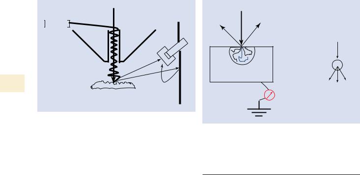
. Fig. 5.27 Currents flowing in and out of the specimen and the electrical junction equivalent
5.4.5\ Specimen Current: The Specimen as Its
Own Detector
zz The Specimen Can Serve as a Perfect Detector for the Total Number of BSE and SE Emitted
Consider the interaction of the beam electrons to produce BSE and SE. For a 20-keV beam incident on copper, about 30 out of 100 beam electrons are backscattered (η = 0.3). The remaining 70 beam electrons lose all their energy in the solid, are reduced to thermal energies, and are captured. Additionally, about 10 units of charge are ejected from copper as secondary electrons (δ = 0.1). This leaves a total of 60 excess electrons in the target. What is the fate of these electrons? To understand this, an alternative view is to consider the electron currents, defined as charge per unit time, which flow in and out of the specimen. Viewed in this fashion, the specimen can be treated as an electrical junction, as illustrated schematically in . Fig. 5.27, and is subject to the fundamental rules which govern junctions in circuits. By Thevinin’s junction theorem, the currents flowing in and out of the junction must exactly balance, or else there will be net accumulation or loss of electrical charge, and the specimen will charge on a macroscopic scale. If the specimen is a conductor or semiconductor and if there is a path to ground from the specimen, then electrical neutrality will be maintained by the flow of a current, designated the “specimen current” (also referred to as the “target current” or “absorbed current”), either to or from ground, depending on the exact conditions of beam energy and specimen composition. What is the magnitude of the specimen current?
Considering the specimen as a junction, the current flowing into the junction is the beam current, iB, and the currents flowing out of the junction are the backscattered electron current, iBS, and the secondary electron current, iSE. For charge balance to occur, the specimen current, iSC, is given by

5.4 · Electron Detectors
iSC = iB − iBS − iSC \ |
(5.15) |
For the copper target, the BSE current will be iBSE = η×iB = 0.3 iB and the SE current will be iSE = δ×iB = 0.1 iB. Substituting
these values in Eq. (5.15) gives the result that the specimen current will be iSC = 0.6 iB, double the largest of the conventional emitted imaging currents, the BSE signal. If a path to ground is not provided so that the specimen current can flow, the specimen will rapidly charge.
Note that in formulating Eq. (5.15) no consideration is given to the large difference in energy carried by the BSE and SE. Since current is the passage of charge per unit time, the ejection of a 1 eV SE from the specimen carries the same weight as a 10 keV BSE in affecting the specimen current signal. Moreover, the specimen current is not sensitive to the direction of emission of BSE and SE, or to their subsequent fate in the SEM specimen chamber, as long as they do not return to the specimen as a result of re-scattering. Thus, specimen current constitutes a signal that is sensitive only to number effects, that is, the total numbers of BSE and SE leaving the specimen.
The specimen serves as its own collector for the specimen current. As such, the specimen current signal is readily available just by insulating the specimen from electrical ground and then measuring the specimen current flowing to ground through a wire to ground. Knowledge of the actual specimen current is extremely useful for establishing consistent operating conditions, and is critical for dose-based X-ray microanalysis. The original beam current itself be measured by creating a “Faraday cup” in the specimen or specimen stage by drilling a blind hole and directing the incident beam into the hole: since no BSE or SE can escape the Faraday cup, the measured specimen current then must equal the beam current. But by measuring the specimen current as a function of the beam position during the scan, an image can be formed that is sensitive to the total emission of BSE and SE regardless of the direction of emission and their subsequent fate interacting with external detectors, the final lens pole piece, and the walls of the specimen chamber. Does the specimen current signal actually convey useful information? As described below under contrast formation, the specimen current signal contains exactly the same information as that carried by the BSE and SE currents. Since external electron detectors measure a convolution of backscattered and/or secondary current with other characteristics such as energy and/or directionality, the specimen current signal can give a unique view of the specimen (Newbury 1976).
To make use of the specimen current signal, the current must be routed through an amplifier on its way to ground. The difficulty is that we must be able to work with a current similar in magnitude to the beam current, without any high gain physical amplification process such as electron-hole pair production in a solid state detector or the electron cascade in an electron multiplier. To achieve acceptable bandwidth at the high gains necessary, most current amplifiers take the form of a low input impedance operational amplifier (Fiori
89 |
|
5 |
|
|
|
et al. 1974). Such amplifiers can operate with currents as low as 10 pA and still provide adequate bandwidth to view acceptable images at slow visual scan rates (one 500-line frame/s).
5.4.6\ A Useful, Practical Measure of a
Detector: Detective Quantum
Efficiency
The geometric efficiency is just one factor in the overall performance of a detector, and while this quantity is relatively straightforward to define in the case of a passive BSE detector, as shown in . Fig. 5.20, it is much more difficult to describe for an E–T detector because of the mix of BSE and direct SE1 and SE2 signal components and the complex conversion and collection of the remote SE3 component produced where BSE strike the objective lens, BSE detector, and chamber walls. A second important factor in detector performance is the efficiency with which each collected electron is converted into useful signal. Thirdly, noise may be introduced at various stages in the amplification process to the digitization which creates the final intensity recorded in the computer memory for the pixel at which the beam dwells.
All of these factors are taken into account by the detective quantum efficiency (DQE). The DQE is a robust measure of detector performance that can be used in the calculation of limitations imposed on imaging through the threshold current/contrast equation (Joy et al. 1996).
The DQE is defined as (Jones 1959)
DQE = (S / N )2experimental / (S / N )2theoretictal \ |
(5.16) |
where S is the signal and N is the noise. Determining the DQE for a detector requires measurement of the experimental S/N ratio as produced under defined conditions of specimen composition, beam current and pixel dwell time that enable an estimate of the corresponding theoretical S/N ratio. This measurement can be performed by imaging a featureless specimen that ideally produces a fixed signal response which translates into a single gray level in the digitally recorded image, giving a direct measure of the signal, S. The corresponding noise, N, is determined from the measured width of the distribution of gray levels around the average value.
Measuring the DQE: BSE Semiconductor Detector
Joy et al. (1996) describe a procedure by which the experimental S/N ratio can be estimated from a digital image of a specimen that produces a unique gray level, so that the broadening observed in the image histogram of the ideal gray level is a quantitative measure of the various noise sources that are inevitable in the total measurement process that produces the image. Thus, the first requirement is a specimen with a highly polished featureless surface that will produce unique values of η and δ and which does not contribute any other sources of

\90 Chapter 5 · Scanning Electron Microscope (SEM) Instrumentation
contrast (e.g., topography, compositional differences, electron channeling, or most problematically, changing δ and η values due to the accumulation of contamination). A polished silicon wafer provides a suitable sample, and with careful precleaning, including plasma cleaning in the SEM airlock if available, the contamination problem can be minimized satisfactorily during the sequence of measurements required. As an alternative to silicon, a metallographically polished (but not etched) pure metallic element (metallic) surface, such as nickel, molybdenum, gold, etc., will be suitable. Because cal-
5 culation of the theoretical S/N ratio is required for the DQE calculation with Eq. 5.16, the beam current must be accurately measured. The SEM must thus be equipped with a picoammeter to measure the beam current, and if an in-column Faraday cup is not available, then a specimen stage Faraday cup (e.g., a blind hole covered with a small [e.g., <100-μm-diameter] aperture) is required to completely capture the beam without loss of BSE or SE so that a measurement of the specimen current equals the beam current.
Because the detector will have a “dark current,” i.e., a response with no beam current, it is necessary to make a series of measurements with changing beam current. It is also important to defeat any automatic image gain scaling that some SEMs provide as a “convenience” feature for the user that acts to automatically compensate for changes in the incident beam current by adjusting the imaging amplifier gain to maintain a steady mid-range gray level.
Measurement sequence
\1.\ Choose a beam current which will serve as the high end of the beam current range, and using the image histogram function, adjust the imaging amplifier controls (often designated “contrast” and “brightness”) to place the average gray level of the specimen near the top of the range, being careful that the upper tail of the gray level distribution of the image of the specimen does not saturate (“clip”) at the maximum gray level (255 for an 8-bit image, 65,535 for a 16-bit image).
\2.\ Keeping the same values for the image amplifier parameters (autoscaling of the imaging amplifier must be defeated before beginning the measurement process), choose a beam current that places the average gray level of the specimen near low end of the gray level range, checking to see that the gray level distribution of the image is completely within the histogram range—that is, there is no clipping of the distribution at the bottom (black) of the range.
\3.\ With the minimum and maximum of the current range established, record a sequence of images with different beam currents between the low and high values and use the image histogram tool to determine the average gray level for each beam current.
\4.\ A graphical plot of data measured with a semiconductor BSE detector for a polished Mo target produces the result illustrated in . Fig. 5.28, where the y-axis intercept value is a measure of the dark current gray level intensity, GLDC (corresponding to zero beam current) of this particular BSE detector.
|
250 |
|
BSE detector |
|
|
|
|
|
|
|
|
|
|
levelGray |
200 |
|
|
|
|
|
150 |
|
|
|
|
|
|
|
|
|
|
|
|
|
|
100 |
|
|
|
|
|
|
50 |
|
|
|
|
|
|
0 |
Y-Intercept = 36 |
|
|
|
|
|
|
|
|
|
|
|
|
0 |
2 |
4 |
6 |
8 |
10 |
Beam current (nA)
. Fig. 5.28 Plot of measured gray level versus incident beam current for a BSE detector. E0 = 20 keV; Mo target
0 |
255 |
Count: 757008 |
Min: 129 |
Mean: 134.117 |
Max: 137 |
StdDev: 0.806 |
Mode: 134 (355350) |
. Fig. 5.29 Output of image histogram from IMAGE-J for the 4 nA image from Fig. 5.28
\5.\ Choose an image recorded within this range and
determine the mean gray level, Gmean, and the variance, Svar (the square of the standard deviation) using the
image histogram function, as shown in . Fig. 5.29.
Calculation sequence:
(S / N )experimental = (GLmean − GLDC ) / Svar |
(5.17) |
|
\ |
where is Svar the variance (the square of the standard deviation) of the gray level distribution. For the values in . Fig. 5.29 for the 4 nA data point obtained with ImageJ-Fiji,
(S / N )experimental |
= (134.3− 36) / 0.5752 = 297.3 |
(5.18) |
|
\ |
|