

- •Preface
- •Imaging Microscopic Features
- •Measuring the Crystal Structure
- •References
- •Contents
- •1.4 Simulating the Effects of Elastic Scattering: Monte Carlo Calculations
- •What Are the Main Features of the Beam Electron Interaction Volume?
- •How Does the Interaction Volume Change with Composition?
- •How Does the Interaction Volume Change with Incident Beam Energy?
- •How Does the Interaction Volume Change with Specimen Tilt?
- •1.5 A Range Equation To Estimate the Size of the Interaction Volume
- •References
- •2: Backscattered Electrons
- •2.1 Origin
- •2.2.1 BSE Response to Specimen Composition (η vs. Atomic Number, Z)
- •SEM Image Contrast with BSE: “Atomic Number Contrast”
- •SEM Image Contrast: “BSE Topographic Contrast—Number Effects”
- •2.2.3 Angular Distribution of Backscattering
- •Beam Incident at an Acute Angle to the Specimen Surface (Specimen Tilt > 0°)
- •SEM Image Contrast: “BSE Topographic Contrast—Trajectory Effects”
- •2.2.4 Spatial Distribution of Backscattering
- •Depth Distribution of Backscattering
- •Radial Distribution of Backscattered Electrons
- •2.3 Summary
- •References
- •3: Secondary Electrons
- •3.1 Origin
- •3.2 Energy Distribution
- •3.3 Escape Depth of Secondary Electrons
- •3.8 Spatial Characteristics of Secondary Electrons
- •References
- •4: X-Rays
- •4.1 Overview
- •4.2 Characteristic X-Rays
- •4.2.1 Origin
- •4.2.2 Fluorescence Yield
- •4.2.3 X-Ray Families
- •4.2.4 X-Ray Nomenclature
- •4.2.6 Characteristic X-Ray Intensity
- •Isolated Atoms
- •X-Ray Production in Thin Foils
- •X-Ray Intensity Emitted from Thick, Solid Specimens
- •4.3 X-Ray Continuum (bremsstrahlung)
- •4.3.1 X-Ray Continuum Intensity
- •4.3.3 Range of X-ray Production
- •4.4 X-Ray Absorption
- •4.5 X-Ray Fluorescence
- •References
- •5.1 Electron Beam Parameters
- •5.2 Electron Optical Parameters
- •5.2.1 Beam Energy
- •Landing Energy
- •5.2.2 Beam Diameter
- •5.2.3 Beam Current
- •5.2.4 Beam Current Density
- •5.2.5 Beam Convergence Angle, α
- •5.2.6 Beam Solid Angle
- •5.2.7 Electron Optical Brightness, β
- •Brightness Equation
- •5.2.8 Focus
- •Astigmatism
- •5.3 SEM Imaging Modes
- •5.3.1 High Depth-of-Field Mode
- •5.3.2 High-Current Mode
- •5.3.3 Resolution Mode
- •5.3.4 Low-Voltage Mode
- •5.4 Electron Detectors
- •5.4.1 Important Properties of BSE and SE for Detector Design and Operation
- •Abundance
- •Angular Distribution
- •Kinetic Energy Response
- •5.4.2 Detector Characteristics
- •Angular Measures for Electron Detectors
- •Elevation (Take-Off) Angle, ψ, and Azimuthal Angle, ζ
- •Solid Angle, Ω
- •Energy Response
- •Bandwidth
- •5.4.3 Common Types of Electron Detectors
- •Backscattered Electrons
- •Passive Detectors
- •Scintillation Detectors
- •Semiconductor BSE Detectors
- •5.4.4 Secondary Electron Detectors
- •Everhart–Thornley Detector
- •Through-the-Lens (TTL) Electron Detectors
- •TTL SE Detector
- •TTL BSE Detector
- •Measuring the DQE: BSE Semiconductor Detector
- •References
- •6: Image Formation
- •6.1 Image Construction by Scanning Action
- •6.2 Magnification
- •6.3 Making Dimensional Measurements With the SEM: How Big Is That Feature?
- •Using a Calibrated Structure in ImageJ-Fiji
- •6.4 Image Defects
- •6.4.1 Projection Distortion (Foreshortening)
- •6.4.2 Image Defocusing (Blurring)
- •6.5 Making Measurements on Surfaces With Arbitrary Topography: Stereomicroscopy
- •6.5.1 Qualitative Stereomicroscopy
- •Fixed beam, Specimen Position Altered
- •Fixed Specimen, Beam Incidence Angle Changed
- •6.5.2 Quantitative Stereomicroscopy
- •Measuring a Simple Vertical Displacement
- •References
- •7: SEM Image Interpretation
- •7.1 Information in SEM Images
- •7.2.2 Calculating Atomic Number Contrast
- •Establishing a Robust Light-Optical Analogy
- •Getting It Wrong: Breaking the Light-Optical Analogy of the Everhart–Thornley (Positive Bias) Detector
- •Deconstructing the SEM/E–T Image of Topography
- •SUM Mode (A + B)
- •DIFFERENCE Mode (A−B)
- •References
- •References
- •9: Image Defects
- •9.1 Charging
- •9.1.1 What Is Specimen Charging?
- •9.1.3 Techniques to Control Charging Artifacts (High Vacuum Instruments)
- •Observing Uncoated Specimens
- •Coating an Insulating Specimen for Charge Dissipation
- •Choosing the Coating for Imaging Morphology
- •9.2 Radiation Damage
- •9.3 Contamination
- •References
- •10: High Resolution Imaging
- •10.2 Instrumentation Considerations
- •10.4.1 SE Range Effects Produce Bright Edges (Isolated Edges)
- •10.4.4 Too Much of a Good Thing: The Bright Edge Effect Hinders Locating the True Position of an Edge for Critical Dimension Metrology
- •10.5.1 Beam Energy Strategies
- •Low Beam Energy Strategy
- •High Beam Energy Strategy
- •Making More SE1: Apply a Thin High-δ Metal Coating
- •Making Fewer BSEs, SE2, and SE3 by Eliminating Bulk Scattering From the Substrate
- •10.6 Factors That Hinder Achieving High Resolution
- •10.6.2 Pathological Specimen Behavior
- •Contamination
- •Instabilities
- •References
- •11: Low Beam Energy SEM
- •11.3 Selecting the Beam Energy to Control the Spatial Sampling of Imaging Signals
- •11.3.1 Low Beam Energy for High Lateral Resolution SEM
- •11.3.2 Low Beam Energy for High Depth Resolution SEM
- •11.3.3 Extremely Low Beam Energy Imaging
- •References
- •12.1.1 Stable Electron Source Operation
- •12.1.2 Maintaining Beam Integrity
- •12.1.4 Minimizing Contamination
- •12.3.1 Control of Specimen Charging
- •12.5 VPSEM Image Resolution
- •References
- •13: ImageJ and Fiji
- •13.1 The ImageJ Universe
- •13.2 Fiji
- •13.3 Plugins
- •13.4 Where to Learn More
- •References
- •14: SEM Imaging Checklist
- •14.1.1 Conducting or Semiconducting Specimens
- •14.1.2 Insulating Specimens
- •14.2 Electron Signals Available
- •14.2.1 Beam Electron Range
- •14.2.2 Backscattered Electrons
- •14.2.3 Secondary Electrons
- •14.3 Selecting the Electron Detector
- •14.3.2 Backscattered Electron Detectors
- •14.3.3 “Through-the-Lens” Detectors
- •14.4 Selecting the Beam Energy for SEM Imaging
- •14.4.4 High Resolution SEM Imaging
- •Strategy 1
- •Strategy 2
- •14.5 Selecting the Beam Current
- •14.5.1 High Resolution Imaging
- •14.5.2 Low Contrast Features Require High Beam Current and/or Long Frame Time to Establish Visibility
- •14.6 Image Presentation
- •14.6.1 “Live” Display Adjustments
- •14.6.2 Post-Collection Processing
- •14.7 Image Interpretation
- •14.7.1 Observer’s Point of View
- •14.7.3 Contrast Encoding
- •14.8.1 VPSEM Advantages
- •14.8.2 VPSEM Disadvantages
- •15: SEM Case Studies
- •15.1 Case Study: How High Is That Feature Relative to Another?
- •15.2 Revealing Shallow Surface Relief
- •16.1.2 Minor Artifacts: The Si-Escape Peak
- •16.1.3 Minor Artifacts: Coincidence Peaks
- •16.1.4 Minor Artifacts: Si Absorption Edge and Si Internal Fluorescence Peak
- •16.2 “Best Practices” for Electron-Excited EDS Operation
- •16.2.1 Operation of the EDS System
- •Choosing the EDS Time Constant (Resolution and Throughput)
- •Choosing the Solid Angle of the EDS
- •Selecting a Beam Current for an Acceptable Level of System Dead-Time
- •16.3.1 Detector Geometry
- •16.3.2 Process Time
- •16.3.3 Optimal Working Distance
- •16.3.4 Detector Orientation
- •16.3.5 Count Rate Linearity
- •16.3.6 Energy Calibration Linearity
- •16.3.7 Other Items
- •16.3.8 Setting Up a Quality Control Program
- •Using the QC Tools Within DTSA-II
- •Creating a QC Project
- •Linearity of Output Count Rate with Live-Time Dose
- •Resolution and Peak Position Stability with Count Rate
- •Solid Angle for Low X-ray Flux
- •Maximizing Throughput at Moderate Resolution
- •References
- •17: DTSA-II EDS Software
- •17.1 Getting Started With NIST DTSA-II
- •17.1.1 Motivation
- •17.1.2 Platform
- •17.1.3 Overview
- •17.1.4 Design
- •Simulation
- •Quantification
- •Experiment Design
- •Modeled Detectors (. Fig. 17.1)
- •Window Type (. Fig. 17.2)
- •The Optimal Working Distance (. Figs. 17.3 and 17.4)
- •Elevation Angle
- •Sample-to-Detector Distance
- •Detector Area
- •Crystal Thickness
- •Number of Channels, Energy Scale, and Zero Offset
- •Resolution at Mn Kα (Approximate)
- •Azimuthal Angle
- •Gold Layer, Aluminum Layer, Nickel Layer
- •Dead Layer
- •Zero Strobe Discriminator (. Figs. 17.7 and 17.8)
- •Material Editor Dialog (. Figs. 17.9, 17.10, 17.11, 17.12, 17.13, and 17.14)
- •17.2.1 Introduction
- •17.2.2 Monte Carlo Simulation
- •17.2.4 Optional Tables
- •References
- •18: Qualitative Elemental Analysis by Energy Dispersive X-Ray Spectrometry
- •18.1 Quality Assurance Issues for Qualitative Analysis: EDS Calibration
- •18.2 Principles of Qualitative EDS Analysis
- •Exciting Characteristic X-Rays
- •Fluorescence Yield
- •X-ray Absorption
- •Si Escape Peak
- •Coincidence Peaks
- •18.3 Performing Manual Qualitative Analysis
- •Beam Energy
- •Choosing the EDS Resolution (Detector Time Constant)
- •Obtaining Adequate Counts
- •18.4.1 Employ the Available Software Tools
- •18.4.3 Lower Photon Energy Region
- •18.4.5 Checking Your Work
- •18.5 A Worked Example of Manual Peak Identification
- •References
- •19.1 What Is a k-ratio?
- •19.3 Sets of k-ratios
- •19.5 The Analytical Total
- •19.6 Normalization
- •19.7.1 Oxygen by Assumed Stoichiometry
- •19.7.3 Element by Difference
- •19.8 Ways of Reporting Composition
- •19.8.1 Mass Fraction
- •19.8.2 Atomic Fraction
- •19.8.3 Stoichiometry
- •19.8.4 Oxide Fractions
- •Example Calculations
- •19.9 The Accuracy of Quantitative Electron-Excited X-ray Microanalysis
- •19.9.1 Standards-Based k-ratio Protocol
- •19.9.2 “Standardless Analysis”
- •19.10 Appendix
- •19.10.1 The Need for Matrix Corrections To Achieve Quantitative Analysis
- •19.10.2 The Physical Origin of Matrix Effects
- •19.10.3 ZAF Factors in Microanalysis
- •X-ray Generation With Depth, φ(ρz)
- •X-ray Absorption Effect, A
- •X-ray Fluorescence, F
- •References
- •20.2 Instrumentation Requirements
- •20.2.1 Choosing the EDS Parameters
- •EDS Spectrum Channel Energy Width and Spectrum Energy Span
- •EDS Time Constant (Resolution and Throughput)
- •EDS Calibration
- •EDS Solid Angle
- •20.2.2 Choosing the Beam Energy, E0
- •20.2.3 Measuring the Beam Current
- •20.2.4 Choosing the Beam Current
- •Optimizing Analysis Strategy
- •20.3.4 Ba-Ti Interference in BaTiSi3O9
- •20.4 The Need for an Iterative Qualitative and Quantitative Analysis Strategy
- •20.4.2 Analysis of a Stainless Steel
- •20.5 Is the Specimen Homogeneous?
- •20.6 Beam-Sensitive Specimens
- •20.6.1 Alkali Element Migration
- •20.6.2 Materials Subject to Mass Loss During Electron Bombardment—the Marshall-Hall Method
- •Thin Section Analysis
- •Bulk Biological and Organic Specimens
- •References
- •21: Trace Analysis by SEM/EDS
- •21.1 Limits of Detection for SEM/EDS Microanalysis
- •21.2.1 Estimating CDL from a Trace or Minor Constituent from Measuring a Known Standard
- •21.2.2 Estimating CDL After Determination of a Minor or Trace Constituent with Severe Peak Interference from a Major Constituent
- •21.3 Measurements of Trace Constituents by Electron-Excited Energy Dispersive X-ray Spectrometry
- •The Inevitable Physics of Remote Excitation Within the Specimen: Secondary Fluorescence Beyond the Electron Interaction Volume
- •Simulation of Long-Range Secondary X-ray Fluorescence
- •NIST DTSA II Simulation: Vertical Interface Between Two Regions of Different Composition in a Flat Bulk Target
- •NIST DTSA II Simulation: Cubic Particle Embedded in a Bulk Matrix
- •21.5 Summary
- •References
- •22.1.2 Low Beam Energy Analysis Range
- •22.2 Advantage of Low Beam Energy X-Ray Microanalysis
- •22.2.1 Improved Spatial Resolution
- •22.3 Challenges and Limitations of Low Beam Energy X-Ray Microanalysis
- •22.3.1 Reduced Access to Elements
- •22.3.3 At Low Beam Energy, Almost Everything Is Found To Be Layered
- •Analysis of Surface Contamination
- •References
- •23: Analysis of Specimens with Special Geometry: Irregular Bulk Objects and Particles
- •23.2.1 No Chemical Etching
- •23.3 Consequences of Attempting Analysis of Bulk Materials With Rough Surfaces
- •23.4.1 The Raw Analytical Total
- •23.4.2 The Shape of the EDS Spectrum
- •23.5 Best Practices for Analysis of Rough Bulk Samples
- •23.6 Particle Analysis
- •Particle Sample Preparation: Bulk Substrate
- •The Importance of Beam Placement
- •Overscanning
- •“Particle Mass Effect”
- •“Particle Absorption Effect”
- •The Analytical Total Reveals the Impact of Particle Effects
- •Does Overscanning Help?
- •23.6.6 Peak-to-Background (P/B) Method
- •Specimen Geometry Severely Affects the k-ratio, but Not the P/B
- •Using the P/B Correspondence
- •23.7 Summary
- •References
- •24: Compositional Mapping
- •24.2 X-Ray Spectrum Imaging
- •24.2.1 Utilizing XSI Datacubes
- •24.2.2 Derived Spectra
- •SUM Spectrum
- •MAXIMUM PIXEL Spectrum
- •24.3 Quantitative Compositional Mapping
- •24.4 Strategy for XSI Elemental Mapping Data Collection
- •24.4.1 Choosing the EDS Dead-Time
- •24.4.2 Choosing the Pixel Density
- •24.4.3 Choosing the Pixel Dwell Time
- •“Flash Mapping”
- •High Count Mapping
- •References
- •25.1 Gas Scattering Effects in the VPSEM
- •25.1.1 Why Doesn’t the EDS Collimator Exclude the Remote Skirt X-Rays?
- •25.2 What Can Be Done To Minimize gas Scattering in VPSEM?
- •25.2.2 Favorable Sample Characteristics
- •Particle Analysis
- •25.2.3 Unfavorable Sample Characteristics
- •References
- •26.1 Instrumentation
- •26.1.2 EDS Detector
- •26.1.3 Probe Current Measurement Device
- •Direct Measurement: Using a Faraday Cup and Picoammeter
- •A Faraday Cup
- •Electrically Isolated Stage
- •Indirect Measurement: Using a Calibration Spectrum
- •26.1.4 Conductive Coating
- •26.2 Sample Preparation
- •26.2.1 Standard Materials
- •26.2.2 Peak Reference Materials
- •26.3 Initial Set-Up
- •26.3.1 Calibrating the EDS Detector
- •Selecting a Pulse Process Time Constant
- •Energy Calibration
- •Quality Control
- •Sample Orientation
- •Detector Position
- •Probe Current
- •26.4 Collecting Data
- •26.4.1 Exploratory Spectrum
- •26.4.2 Experiment Optimization
- •26.4.3 Selecting Standards
- •26.4.4 Reference Spectra
- •26.4.5 Collecting Standards
- •26.4.6 Collecting Peak-Fitting References
- •26.5 Data Analysis
- •26.5.2 Quantification
- •26.6 Quality Check
- •Reference
- •27.2 Case Study: Aluminum Wire Failures in Residential Wiring
- •References
- •28: Cathodoluminescence
- •28.1 Origin
- •28.2 Measuring Cathodoluminescence
- •28.3 Applications of CL
- •28.3.1 Geology
- •Carbonado Diamond
- •Ancient Impact Zircons
- •28.3.2 Materials Science
- •Semiconductors
- •Lead-Acid Battery Plate Reactions
- •28.3.3 Organic Compounds
- •References
- •29.1.1 Single Crystals
- •29.1.2 Polycrystalline Materials
- •29.1.3 Conditions for Detecting Electron Channeling Contrast
- •Specimen Preparation
- •Instrument Conditions
- •29.2.1 Origin of EBSD Patterns
- •29.2.2 Cameras for EBSD Pattern Detection
- •29.2.3 EBSD Spatial Resolution
- •29.2.5 Steps in Typical EBSD Measurements
- •Sample Preparation for EBSD
- •Align Sample in the SEM
- •Check for EBSD Patterns
- •Adjust SEM and Select EBSD Map Parameters
- •Run the Automated Map
- •29.2.6 Display of the Acquired Data
- •29.2.7 Other Map Components
- •29.2.10 Application Example
- •Application of EBSD To Understand Meteorite Formation
- •29.2.11 Summary
- •Specimen Considerations
- •EBSD Detector
- •Selection of Candidate Crystallographic Phases
- •Microscope Operating Conditions and Pattern Optimization
- •Selection of EBSD Acquisition Parameters
- •Collect the Orientation Map
- •References
- •30.1 Introduction
- •30.2 Ion–Solid Interactions
- •30.3 Focused Ion Beam Systems
- •30.5 Preparation of Samples for SEM
- •30.5.1 Cross-Section Preparation
- •30.5.2 FIB Sample Preparation for 3D Techniques and Imaging
- •30.6 Summary
- •References
- •31: Ion Beam Microscopy
- •31.1 What Is So Useful About Ions?
- •31.2 Generating Ion Beams
- •31.3 Signal Generation in the HIM
- •31.5 Patterning with Ion Beams
- •31.7 Chemical Microanalysis with Ion Beams
- •References
- •Appendix
- •A Database of Electron–Solid Interactions
- •A Database of Electron–Solid Interactions
- •Introduction
- •Backscattered Electrons
- •Secondary Yields
- •Stopping Powers
- •X-ray Ionization Cross Sections
- •Conclusions
- •References
- •Index
- •Reference List
- •Index
369 |
22 |
22.3 · Challenges and Limitations of Low Beam Energy X-Ray Microanalysis
Counts
80000 |
|
|
|
|
|
|
|
|
|
Fe3N_5kV25nA13%DT |
|
|
|
|
|
|
|
|
|
|
|
|
|
Residual_Fe3N_5kV25nA13%DT |
|
||
|
|
|
|
|
|
E0 = 5 keV |
|
|
|
|
|
|
|
60000 |
|
|
|
|
|
Fe3N |
|
|
|
|
|
|
|
|
|
|
|
|
Fitting residual |
|
|
|
|
|
|
||
40000 |
|
|
|
|
|
|
|
|
|
|
|
|
|
20000 |
|
|
|
|
|
|
|
|
|
|
|
|
|
0 |
|
|
|
|
|
|
|
|
|
|
|
|
|
|
|
|
|
|
|
|
|
|
|
|
|
|
|
0.00 |
0.10 |
0.20 |
0.30 |
0.40 |
0.50 |
0.60 |
0.70 |
0.80 |
0.90 |
1.00 |
|||
|
|
|
|
|
|
Photon energy (keV) |
|
|
|
|
|
||
. Fig. 22.13 EDS spectrum of iron nitride, Fe3N and residual after peak fitting for N and Fe; E0 = 5 keV
Counts
|
|
|
|
|
|
|
|
|
|
|
Cu2O_5kV25nA5%DT |
|
|
250000 |
|
|
|
|
|
|
|
|
|
|
CuO_5kV25nA5%DT |
|
|
|
|
|
|
|
|
|
E0 = 5 keV |
|
|
|
|
|
|
|
|
|
|
|
|
|
|
|
|
|
|
|
|
200000 |
|
|
|
|
|
|
|
Cu2O |
|
|
|
|
|
|
|
|
|
|
|
|
CuO |
|
|
|
|
|
|
150000 |
|
|
|
|
|
|
|
|
|
|
|
|
|
100000 |
|
|
|
|
|
|
|
|
|
|
|
|
|
50000 |
|
|
|
|
|
|
|
|
|
|
|
|
|
0 |
|
|
|
|
|
|
|
|
|
|
|
|
|
|
|
|
|
|
|
|
|
|
|
|
|
|
|
0.0 |
0.2 |
0.4 |
0.6 |
0.8 |
1.0 |
1.2 |
1.4 |
1.6 |
1.8 |
2.0 |
|||
Photon energy (keV)
. Fig. 22.14 EDS spectra of copper oxides, Cu2O and CuO; E0 = 5 keV
22.3\ Challenges and Limitations of Low
Beam Energy X-Ray Microanalysis
22.3.1\ Reduced Access to Elements
High performance SEMs can routinely operate with the beam energy as low as 500 eV; and with special electron optics and/or stage biasing, the landing kinetic energy of the beam can be reduced to 10 eV. Because the beam penetration depth decreases rapidly as the incident energy is reduced, as shown in . Fig. 22.9, which plots the Kanaya– Okayama range for 0 – 5 keV, low kinetic energy provides extreme sensitivity to the surface of the specimen, which
can improve the contrast from surface features of interest. Since the lateral ranges over which the backscattered electron (BSE) and closely related SE2 signals are emitted are also greatly restricted at low beam energies, these signals closely approach the beam footprint of SE1 emission and thus contribute to high spatial resolution imaging rather than degrading resolution as they do at high beam energy.
Thus, low beam energy operation has strong advantages for SEM imaging down to beam landing energies of tens of eV.
While low beam energy SEM imaging can exploit the full range of landing kinetic energies to seek to maximize contrast from surface features of interest, the situation for
\370 Chapter 22 · Low Beam Energy X-Ray Microanalysis
low beam energy X-ray microanalysis is much more constrained. As discussed above, as the beam energy is reduced, the atomic shells that can be ionized become more restricted. A beam energy of 5 keV is the lowest energy that provides access to measureable X-rays for elements of the periodic table from Z = 3 (Li) to Z = 94 (Pu), as shown in
. Fig. 22.5. If the beam energy is reduced to E0 = 2.5 keV, EDS X-ray microanalysis of large portions of the periodic table is no longer possible because no atomic shell with useful X-ray yield can be excited or effectively measured for these elements, creating the situation shown in . Fig. 22.6. Further decreases in the beam energy results in losing access to even more elements, with only about half of the elements measureable at E0 = 1 keV, and many of those only marginally so.
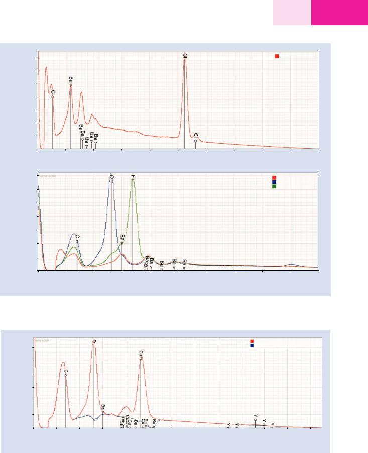
Even to achieve the elemental coverage depicted for E0 = 5 keV in . Fig. 22.5, low beam energy EDS X-ray microanalysis requires measurement of characteristic X-rays that are not normally utilized in conventional beam energy analysis for certain elements. Thus Ti must be measured with the Ti L-family when E0 ≤ 5 keV, as shown in . Fig. 22.15. Similarly, for Ba, the Ba L-family around 4.5 keV is the usual choice for microanalysis, but the Ba L3 excitation energy is 5.25 keV, and thus the Ba L-family not excited with E0 = 5 keV, forcing the analyst to utilize the Ba M-family. The EDS
spectrum of BaCl2 with E0 = 5 keV is shown in . Fig. 22.16. Due to the low fluorescence yield of ionizations in the Ba M-shell, the Ba M-family peaks are seen to have a relatively low peak-to-background, despite Ba being present in this case as a major constituent (mass concentration C = 0.696), making the measurement of Ba when present as a minor to trace constituent even more problematic. A practical problem that arises when analyzing with the Ba M-family peaks is the difficulty in obtaining suitable Ba M-family peak references that are free of interferences from other elements. While BaCl2 is interference-free in the Ba M-family region, BaF2 and BaCO3 are not, as shown in . Fig. 22.16. However, BaCl2 shows evidence of degradation under the electron beam, possibly changing the local compositions and thus disqualifying it as a standard. Despite degradation under the beam, BaCl2 can serve as a peak reference, while BaF2 or another Ba-containing compound or glass that is stable under electron bombardment can serve as a standard. Despite these challenges, successful analysis of the high transition temperature superconducting material YBa2Cu3O7-X at E0 = 2.5 keV with CuO, Y2O3, and BaF2 as the standard and BaCl2 as the peak reference is demonstrated in . Fig. 22.17 and . Table 22.5, where analyses with oxygen done directly against a standard (ZnO) and by the method of assumed oxygen stoichiometry of the cations are presented.
Counts
Ti_5kV30nA3%DT
50000 |
|
|
|
|
|
|
|
|
|
|
|
|
|
|
|
|
|
Ti |
|
|
|
|
|
|
|
40000 |
|
|
|
|
E0 = 5 keV |
|
|
|
|
|
|
|
30000 |
|
|
|
|
|
|
|
|
|
|
|
|
20000 |
|
|
|
|
|
|
|
|
|
|
|
|
10000 |
|
|
|
|
|
|
|
|
|
|
|
|
0 |
|
|
|
|
|
|
|
|
|
|
|
|
|
|
|
|
|
|
|
|
|
|
|
|
|
0.0 |
0.2 |
0.4 |
0.6 |
0.8 |
1.0 |
1.2 |
1.4 |
1.6 |
1.8 |
2.0 |
||
Photon energy (keV)
. Fig. 22.15 EDS spectrum of titanium; E0 = 5 keV
22
371 |
22 |
22.3 · Challenges and Limitations of Low Beam Energy X-Ray Microanalysis
Counts
Counts
35000
30000
25000
20000
15000
10000
5000
0 
0.0
140000
120000
100000
80000
60000
40000
20000
0
0.0
BaCl2_5kV25nA4%DT
BaCl2
E0 = 5 keV
0.5 |
1.0 |
1.5 |
2.0 |
2.5 |
3.0 |
3.5 |
4.0 |
4.5 |
5.0 |
Photon energy (keV)
BaCl2_5kV25nA4%DT
BaCO3_5kV30nA4%DT
BaF2_5kV30nA4%DT
E0 = 5 keV
BaCl2
BaF2
BaCO3
0.2 |
0.4 |
0.6 |
0.8 |
1.0 |
1.2 |
1.4 |
1.6 |
1.8 |
2.0 |
|
|
|
|
Photon energy (keV) |
|
|
|
|
|
. Fig. 22.16 EDS spectrum of barium chloride, showing the Ba M-family (upper); EDS spectra of BaCl2, BaF2, and BaCO3 (lower); E0 = 5 keV
Counts
|
|
|
|
|
|
|
|
|
|
|
|
123TC_2.5kV50nA3%DT |
|
|
60000 |
|
|
|
|
|
|
|
|
|
|
|
Residual_123TC_2.5kV50nA3%DT |
||
|
|
|
|
|
|
|
|
|
|
|
|
|
|
|
50000 |
|
|
|
|
|
|
|
E0 =2.5 keV |
|
|
|
|
|
|
|
|
|
|
|
|
|
YBa2Cu3O7-X |
|
|
|
|
|
||
40000 |
|
|
|
|
|
|
|
Fitting residual |
|
|
|
|
|
|
|
|
|
|
|
|
|
|
|
|
|
|
|
|
|
30000 |
|
|
|
|
|
|
|
|
|
|
|
|
|
|
20000 |
|
|
|
|
|
|
|
|
|
|
|
|
|
|
10000 |
|
|
|
|
|
|
|
|
|
|
|
|
|
|
0 |
|
|
|
|
|
|
|
|
|
|
|
|
|
|
|
|
|
|
|
|
|
|
|
|
|
|
|
|
|
0.0 |
0.2 |
0.4 |
0.6 |
0.8 |
1.0 |
1.2 |
1.4 |
1.6 |
1.8 |
2.0 |
2.2 |
2.4 |
||
Photon energy (keV)
. Fig. 22.17 EDS spectrum of YBa2Cu3O7-X, and residual after peak fitting for O K-L2, the Ba M-family and Cu L-family; E0 = 2.5 keV
372\ |
Chapter 22 · Low Beam Energy X-Ray Microanalysis |
|
|
|
|
||
|
|
|
|
|
|
||
|
. Table 22.5 Analysis of YBa2Cu3O7-X at E0 = 2.5 keV |
|
|
|
|
||
|
|
|
|
|
|
|
|
|
Element |
Cav mass conc |
RDEV % |
σrel, % |
Cav mass conc |
RDEV % |
σrel, % |
|
|
|
−6.4 |
|
|
|
|
|
O |
0.1574 (stoich) |
1.1 |
0.1787 (ZnO) |
6.3 |
1.3 |
|
|
Cu |
0.2910 |
1.7 |
3.4 |
0.3024 |
5.7 |
1.4 |
|
Y |
0.1296 |
−2.9 |
3.1 |
0.1322 |
−0.90 |
2.4 |
|
Ba |
0.4220 |
2.4 |
3.6 |
0.3867 |
−6.2 |
2.3 |
22.3.2\ Relative Depth of X-Ray Generation:
Susceptibility to Vertical
Heterogeneity
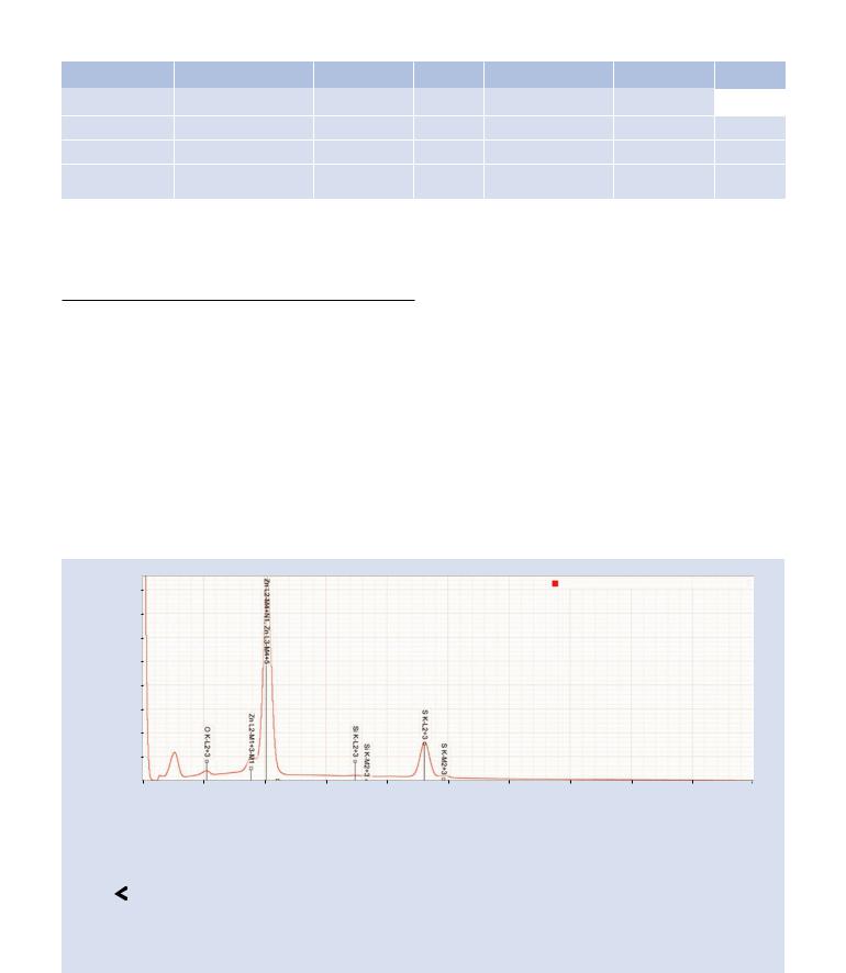
Another challenge in low beam energy X-ray microanalysis is that the difference in the depth of generation and sampling of characteristic X-rays from different elements imposes strong requirements on the homogeneity of the specimen along the beam axis. While the physics of characteristic X-ray generation is such that relative differences in the generation and emission of X-rays occur at all beam energies, including the conventional beam energy range, in the low beam energy analysis region the effect is exacerbated due to the rapidly changing range as described by Eq. (22.5). It is useful to consider that the photon energy axis of an EDS spectrum can also be thought of as a range axis that describes the depth to
which a given photon energy can be generated. Such a range scale is shown parallel to the photon energy axis in . Fig. 22.18 for a ZnS target with E0 = 5 keV. Points on the Kanaya– Okayama range scale corresponding to exciting X-rays with ionization energies of 4 keV, 3 keV, 2 keV and 1 keV are noted. The range scale is non-linear when compared to the energy scale due to the E01.67 term in the range equation. In ZnS, S K (Ec = 2.47 keV) can be excited to a depth of approximately 0.21 μm, while Zn (Ec = 1.02 keV) continues to a depth of 0.28 μm. If the ZnS contained Ca as a trace or minor constituent, it would only be generated to a depth of 0.09 μm. Thus, if quantitative analysis is to be successful by means of the k-ratio/matrix corrections protocol performed at a single beam energy in the low beam energy regime, the material must be homogeneous from the surface to the full range of the excited volume.
Counts
400000 |
|
|
|
|
|
|
|
|
ZnS_5kV50nAMED5eV51kHz10DT_100s |
|
|
||
|
|
|
|
|
|
|
|
|
|
|
|
|
|
350000 |
|
|
|
|
|
|
|
ZnS |
|
|
|
|
|
|
|
|
|
|
|
|
|
|
|
|
|
|
|
300000 |
|
|
|
|
|
|
|
E0 = 5 keV |
|
|
|
|
|
250000 |
|
|
|
|
|
|
|
|
|
|
|
|
|
200000 |
|
|
|
|
|
|
|
|
|
|
|
|
|
150000 |
|
|
|
|
|
|
|
|
|
|
|
|
|
100000 |
|
|
|
|
|
|
|
|
|
|
|
|
|
50000 |
|
|
|
|
|
|
|
|
|
|
|
|
|
0 |
|
|
|
|
|
|
|
|
|
|
|
|
|
|
|
|
|
|
|
|
|
|
|
|
|
|
|
0 |
500 |
1000 |
1500 |
2000 |
2500 |
3000 |
3500 |
4000 |
4500 |
5000 |
|||
|
|
|
|
|
|
Photon energy (eV) |
|
|
|
|
|
|
|
|
|
|
Zn L (Ec=1.02 keV) |
|
|
S K (Ec=2.47 keV) |
|
|
Ca K (Ec=4.04 keV) |
|
|
||
|
|
|
0.28 µm |
|
|
|
0.21 µm |
|
|
0.090 µm |
|
|
|
|
|
|
|
|
|
|
|
|
|
|
|
|
|
|
|
|
|
|
|
|
|
|
|
|
|
|
|
|
|
|
|
|
|
|
|
|
|
|
|
|
|
|
|
|
|
|
|
|
|
|
|
22 |
|
|
|
|
|
|
|
|
|
|
|
|
0.28 |
0.24 |
0.17 |
0.094 |
0.0 |
||||||||
|
|
|
|
|
|
|
|
|
|
|
|
|
Kanaya-Okayama range (µm) for X-ray production in ZnS at E0 = 5 keV
. Fig. 22.18 EDS spectrum of ZnS illustrating concept of the energy axis of the spectrum and the corresponding depth of X-ray generation; E0 = 5 keV