

Fundamentals of Microelectronics
.pdfBR |
Wiley/Razavi/Fundamentals of Microelectronics [Razavi.cls v. 2006] |
June 30, 2007 at 13:42 |
541 (1) |
|
|
|
|
Sec. 11.1 Fundamental Concepts 541
Solution
From Eq. (11.1), we have
H(s) = |
Vout (s) = ,g |
|
(R |
|
jj |
1 |
) |
(11.4) |
|
m |
D |
|
|||||||
|
Vin |
|
|
CLs |
|
|
|||
|
= |
,gmRD |
: |
|
(11.5) |
||||
|
|
RDCLs + 1 |
|
|
|||||
For a sinusoidal input, we replace s = j! and compute the magnitude of the transfer function:3
|
|
|
|
|
|
Vout |
= |
|
|
|
|
gmRD |
|
|
: |
(11.6) |
||||
|
|
|
|
|
|
|
|
|
|
|
|
|
|
|
|
|
|
|||
|
|
|
|
|
|
Vin |
|
pRD2 CL2 !2 + 1 |
|
|||||||||||
As expected, the gain begins at gmRD at low frequencies, rolling off as R2 C2 !2 becomes |
||||||||||||||||||||
comparable with unity. At ! = 1=(RDCL), |
|
|
|
|
|
|
|
|
|
|
|
D |
L |
|||||||
|
|
|
|
|
|
|
|
|
|
|
|
|
||||||||
|
|
|
|
|
|
|
Vout |
|
|
|
|
gmRD |
|
|
|
(11.7) |
||||
|
|
|
|
|
|
|
Vin |
= |
|
p |
|
|
|
: |
|
|
||||
|
|
|
|
|
|
|
|
|
|
|
2 |
|
|
|
|
|
||||
Since 20 log p |
|
3 dB, we say the ,3-dB bandwidth |
of the circuit is equal to 1=(RDCL) (Fig. |
|||||||||||||||||
2 |
||||||||||||||||||||
11.6). |
|
|
|
|
|
|
|
|
|
|
|
|
|
|
|
|
|
|
|
|
|
|
Vout |
|
|
−3−dB |
|
|
|
|
|
|
|
|
|
|
|
|
|
||
|
|
|
|
|
|
Bandwidth |
|
|
−3−dB |
|
||||||||||
|
|
|
Vin |
|
|
|
||||||||||||||
|
|
|
|
|
|
|
|
|
|
|
|
|
|
|||||||
|
|
|
|
|
|
|
|
|
|
|
|
|
Rolloff |
|
||||||
|
|
|
|
|
|
|
|
|
|
|
|
|
|
|
||||||
|
|
|
|
|
|
|
|
|
|
|
|
|
|
|
|
|
|
|||
|
|
|
|
|
|
|
|
|
1 |
|
|
|
|
|
ω |
|
||||
R D CL
Figure 11.6
Exercise
Derive the above results if 6= 0.
Example 11.5
Consider the common-emitter stage shown in Fig. 11.7. Derive a relationship between the gain, the ,3-dB bandwidth, and the power consumption of the circuit. Assume VA = 1.
Solution
In a manner similar to the CS topology of Fig. 11.5(a), the bandwidth is given by 1=(RCCL), the low-frequency gain by gmRC = (IC =VT )RC, and the power consumption by IC VCC. For the highest performance, we wish to maximize both the gain and the bandwidth (and hence the
3The magnitude of the complex number a + jb is equal to pa2 + b2.
BR |
Wiley/Razavi/Fundamentals of Microelectronics [Razavi.cls v. 2006] |
June 30, 2007 at 13:42 |
542 (1) |
|
|
|
|
542 |
Chap. 11 |
Frequency Response |
VCC
R C 
 Vout
Vout
Vin

 Q 1
Q 1  CL
CL
Figure 11.7
product of the two) and minimize the power dissipation. We therefore define a “figure of merit” as
|
|
IC |
RC |
1 |
|
|||
Gain Bandwidth |
= |
VT |
RCCL |
(11.8) |
||||
Power Consumption |
|
|
IC VCC |
|
||||
|
= |
|
1 |
|
|
1 |
: |
(11.9) |
|
|
|
|
|
|
|||
|
|
VT |
VCC CL |
|
||||
Thus, the overall performance can be improved by lowering (a) the temperature;4 (b) VCC but at the cost of limiting the voltage swings; or (c) the load capacitance. In practice, the load capacitance receives the greatest attention. Equation (11.9) becomes more complex for CS stages (Problem 15).
Exercise
Derive the above results if VA < 1.
Example 11.6
Explain the relationship between the frequency response and step response of the simple lowpass filter shown in Fig. 11.4(a).
Solution
To obtain the transfer function, we view the circuit as a voltage divider and write
|
|
|
|
|
1 |
|
|
|
|
|
Vout (s) = |
|
|
|
|
|
|
|
|
H(s) = |
|
|
C1s |
|
(11.10) |
||||
1 |
|
|
|
|
|
||||
|
Vin |
|
+ R1 |
|
|
||||
|
|
|
C1s |
|
|
||||
|
= |
|
|
|
1 |
|
|
: |
(11.11) |
|
|
||||||||
|
R1C1s + 1 |
||||||||
The frequency response is determined by replacing s with j! and computing the magnitude:
jH(s = j!)j = |
|
|
1 |
|
|
|
: |
(11.12) |
|
|
|
|
|
|
|||
2 |
2 |
|
2 |
|
||||
|
|
|
|
|
||||
|
pR1C1 |
! |
|
+ 1 |
|
|||
4For example, by immersing the circuit in liquid nitrogen (T = 77 K), but requiring that the user carry a tank around!
BR |
Wiley/Razavi/Fundamentals of Microelectronics [Razavi.cls v. 2006] |
June 30, 2007 at 13:42 |
543 (1) |
|
|
|
|
Sec. 11.1 |
Fundamental Concepts |
543 |
||
The ,3-dB bandwidth is equal to 1=(R1C1). |
|
|||
The circuit's response to a step of the form V0u(t) is given by |
|
|||
|
Vout(t) = V0(1 , exp |
,t |
)u(t): |
(11.13) |
|
|
R1C1 |
|
|
The relationship between (11.12) and (11.13) is that, as R1C1 increases, the bandwidth drops and the step response becomes slower. Figure 11.8 plots this behavior, revealing that a narrow bandwidth results in a sluggish time response. This observation explains the effect seen in Fig.
H |
R 1C1 |
|
1.0 |
R 1C1 |
Vout |
|
f |
t |
|
(a) |
(b) |
Figure 11.8
11.3(b): since the signal cannot rapidly jump from low (white) to high (black), it spends some time at intermediate levels (shades of gray), creating “fuzzy” edges.
Exercise
At what frequency does jHj fall by a factor of two?
11.1.3 Bode's Rules
The task of obtaining jH(j!)j from H(s) and plotting the result is somewhat tedious. For this reason, we often utilize Bode's rules (approximations) to construct jH(j!)j rapidly. Bode's rules for jH(j!)j are as follows:
As ! passes each pole frequency, the slope of jH(j!)j decreases by 20 dB/dec; (A slope of 20 dB/dec simply means a tenfold change in H for a tenfold increase in frequency.)
As ! passes each zero frequency, the slope of jH(j!)j increases by 20 dB/dec.5
Example 11.7
Construct the Bode plot of jH(j!)j for the CS stage depicted in Fig. 11.5(a).
Solution
Equation (11.5) indicates a pole frequency of
j!p1j = |
1 |
: |
(11.14) |
|
|
||||
RDCL |
||||
|
|
|
The magnitude thus begins at gmRD at low frequencies and remains flat up to ! = j!p1j. At this point, the slope changes from zero to ,20 dB/dec. Figure 11.9 illustrates the result. In contrast
5Complex poles may result in sharp peaks in the frequency response, an effect neglected in Bode's approximation.
BR |
Wiley/Razavi/Fundamentals of Microelectronics [Razavi.cls v. 2006] |
June 30, 2007 at 13:42 |
544 (1) |
|
|
|
|
544 |
Chap. 11 |
Frequency Response |
to Fig. 11.5(b), the Bode approximation ignores the 3-dB roll-off at the pole frequency—but
it greatly simplifies the algebra. As evident from Eq. (11.6), for R2 C2 !2
D L
provides a good approximation.
20log Vout
Vin g m RD
Figure 11.9
− 20
dB/dec ωp1 log ω
Exercise
Construct the Bode plot for gm = (150 ),1; RD = 2 k , and CL = 100 fF.
11.1.4 Association of Poles with Nodes
The poles of a circuit's transfer function play a central role in the frequency response. The designer must therefore be able to identify the poles intuitively so as to determine which parts of the circuit appear as the “speed bottleneck.”
The CS topology studied in Example 11.4 serves as a good example for identifying poles by inspection. Equation (11.5) reveals that the pole frequency is given by the inverse of the product of the total resistance seen between the output node and ground and the total capacitance seen between the output node and ground. Applicable to many circuits, this observation can be generalized as follows: if node j in the signal path exhibits a small-signal resistance of Rj to ground and a capacitance of Cj to ground, then it contributes a pole of magnitude (Rj Cj ),1 to the transfer function.
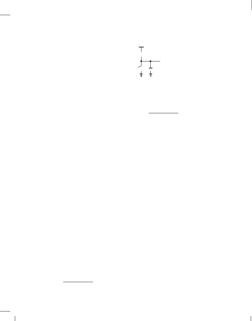
Example 11.8
Determine the poles of the circuit shown in Fig. 11.10. Assume = 0
VDD
R D
 Vout
Vout
RS
Vin


 M 1
M 1  CL
CL
 Cin
Cin
Figure 11.10 .
Solution
Setting Vin to zero, we recognize that the gate of M1 sees a resistance of RS and a capacitance of Cin to ground. Thus,
j!p1j = |
1 |
: |
(11.15) |
|
|
||||
RSCin |
||||
|
|
|
BR |
Wiley/Razavi/Fundamentals of Microelectronics [Razavi.cls v. 2006] |
June 30, 2007 at 13:42 |
545 (1) |
|
|
|
|
Sec. 11.1 |
Fundamental Concepts |
545 |
We may call !p1 the “input pole” to indicate that it arises in the input network. Similarly, the “output pole” is given by
j!p2j = |
1 |
: |
(11.16) |
|
|
||||
RDCL |
||||
|
|
|
Since the low-frequency gain of the circuit is equal to ,gmRD, we can readily write the magnitude of the transfer function as:
|
Vout |
|
= |
|
|
gmRD |
|
|
: |
(11.17) |
|
|
|
|
|
|
|
|
|
||||
|
Vin |
|
q |
2 |
2 |
2 |
2 |
||||
|
|
|
|||||||||
|
|
|
|
|
(1 + ! |
=!p1)(1 + ! |
!p2) |
|
|||
Exercise
If !p1 = !p2, at what frequency does the gain drop by 3 dB?
Example 11.9
Compute the poles of the circuit shown in Fig. 11.11. Assume = 0.
VDD
 RD
RD
 Vout
Vout
M 1 |
|
|
|
Vb |
|
|
CL |
|
|
|
|
|
|||
|
|
|
|
|
|||
RS |
|
|
|
|
|
|
|
|
|
|
|
|
|
|
Vin
 Cin
Cin
Figure 11.11 .
Solution
With Vin = 0, the small-signal resistance seen at the source of M1 is given by RSjj(1=gm), yielding a pole at
!p1 = |
1 |
|
: |
(11.18) |
|
|
|
|
|||
1 |
|
||||
|
|
|
|
||
|
RSjj |
|
Cin |
|
|
|
gm |
|
|
||
The output pole is given by !p2 = (RDCL),1.
Exercise
How do we choose the value of RD such that the output pole frequency is ten times the input pole frequency?
BR |
Wiley/Razavi/Fundamentals of Microelectronics [Razavi.cls v. 2006] |
June 30, 2007 at 13:42 |
546 (1) |
|
|
|
|
546 |
Chap. 11 |
Frequency Response |
The reader may wonder how the foregoing technique can be applied if a node is loaded with a “floating” capacitor, i.e., a capacitor whose other terminal is also connected to a node in the signal path (Fig. 11.12). In general, we cannot utilize this technique and must write the circuit's equations and obtain the transfer function. However, an approximation given by “Miller's Theorem” can simplify the task in some cases.
|
VDD |
|
R D |
|
CF |
RS |
Vout |
Vin |
M 1 |
Figure 11.12 Circuit with floating capacitor.
11.1.5 Miller's Theorem
Our above study and the example in Fig. 11.12 make it desirable to obtain a method that “transforms” a floating capacitor to two grounded capacitors, thereby allowing association of one pole with each node. Miller's theorem is such a method. Miller's theorem, however, was originally conceived for another reason. In the late 1910s, John Miller had observed that parasitic capacitances appearing between the input and output of an amplifier may drastically lower the input impedance. He then proposed an analysis that led to the theorem.
Consider the general circuit shown in Fig. 11.13(a), where the floating impedance, ZF , ap-
1 |
Z F |
2 |
1 |
2 |
|
V1 |
|
V2 |
|
|
|
|
|
Z 1 |
V1 |
V2 |
Z 2 |
|
(a) |
|
|
(b) |
|
Figure 11.13 (a) General circuit including a floating impedance, (b) equivalent of (a) as obtained from Miller's theorem.
pears between nodes 1 and 2. We wish to transform ZF to two grounded impedances as depicted in Fig. 11.13(b), while ensuring all of the currents and voltages in the circuit remain unchanged. To determine Z1 and Z2, we make two observations: (1) the current drawn by ZF from node 1 in Fig. 11.13(a) must be equal to that drawn by Z1 in Fig. 11.13(b); and (2) the current injected to node 2 in Fig. 11.13(a) must be equal to that injected by Z2 in Fig. 11.13(b). (These requirements guarantee that the circuit does not “feel” the transformation.) Thus,
V1 |
, V2 |
= |
V1 |
(11.19) |
||
ZF |
|
Z1 |
|
|||
V1 |
, V2 |
= , |
V2 |
: |
(11.20) |
|
|
|
|||||
ZF |
|
|
Z2 |
|
||
Denoting the voltage gain from node 1 to node 2 by Av, we obtain
Z1 = ZF |
|
V1 |
(11.21) |
|
|
|
|||
V1 |
, V2 |
|||
|
|
BR |
Wiley/Razavi/Fundamentals of Microelectronics [Razavi.cls v. 2006] |
June 30, 2007 at 13:42 |
547 (1) |
|
|
|
|
Sec. 11.1 Fundamental Concepts |
|
|
|
|
|
|
|
= |
|
ZF |
|
|
|
|
|
1 , Av |
|
||||||
|
|
||||||
and |
|
|
|
|
|
|
|
Z2 = Z |
|
,V2 |
|||||
|
F V1 |
, V2 |
|||||
= |
|
ZF |
|
|
|
: |
|
|
1 |
|
|
||||
|
|
|
|
|
|||
|
1 , |
|
|
|
|||
|
Av |
|
|||||
547
(11.22)
(11.23)
(11.24)
Called Miller's theorem, the results expressed by (11.22) and (11.24) prove extremely useful in analysis and design. In particular, (11.22) suggests that the floating impedance is reduced by a factor of 1 , Av when “seen” at node 1.
As an important example of Miller's theorem, let us assume ZF is a single capacitor, CF , tied between the input and output of an inverting amplifier [Fig. 11.14(a)]. Applying (11.22), we have
Z1 = |
ZF |
|
|
(11.25) |
1 , Av |
|
|||
|
|
|
||
= |
1 |
; |
(11.26) |
|
|
||||
(1 + A0)CF s |
||||
where the substitution Av = ,A0 is made. What type of impedance is Z1? The 1=s dependence suggests a capacitor of value (1 + A0)CF , as if CF is “amplified” by a factor of 1 + A0. In other words, a capacitor CF tied between the input and output of an inverting amplifier with a gain of A0 raises the input capacitance by an amount equal to (1 + A0)CF . We say such a circuit suffers from “Miller multiplication” of the capacitor.
CF
Vin |
− A 0 |
Vout |
V |
|
− A 0 V |
CF
Vin |
− A 0 |
Vout |
( 1 + A 0 |
( |
CF ( 1 + |
1
A 0
(
(a) |
(b) |
Figure 11.14 (a) Inverting circuit with floating capacitor, (b) equivalent circuit as obtained from Miller's theorem.
The effect of CF at the output can be obtained from (11.24):
Z2 = |
ZF |
|
|
|
|
|
(11.27) |
|
1 |
|
|
|
|
||||
|
|
|
|
|
|
|||
|
1 , |
|
|
|
|
|
||
|
Av |
|
|
|
||||
= |
|
|
1 |
|
; |
(11.28) |
||
1 + |
|
|
|
|
||||
|
1 |
CF s |
|
|||||
|
A0 |
|
||||||
which is close to (CF s),1 if A0 1. Figure 11.14(b) summarizes these results.
The Miller multiplication of capacitors can also be explained intuitively. Suppose the input voltage in Fig. 11.14(a) goes up by a small amount V . The output then goes down by A0 V . That is, the voltage across CF increases by (1 + A0) V , requiring that the input provide a
BR |
Wiley/Razavi/Fundamentals of Microelectronics [Razavi.cls v. 2006] |
June 30, 2007 at 13:42 |
548 (1) |
|
|
|
|
548 |
Chap. 11 |
Frequency Response |
proportional charge. By contrast, if CF were not a floating capacitor and its right plate voltage did not change, it would experience only a voltage change of V and require less charge.
The above study points to the utility of Miller's theorem for conversion of floating capacitors to grounded capacitors. The following example demonstrates this principle.
Example 11.10
Estimate the poles of the circuit shown in Fig. 11.15(a). Assume = 0.
|
VDD |
|
VDD |
|
R D |
|
R D |
|
CF |
|
|
|
|
Vout |
|
RS |
Vout |
|
|
|
RS |
||
Vin |
M 1 |
Vin |
M 1 Cout |
|
|
|
Cin |
|
(a) |
|
(b) |
Figure 11.15
Solution
Noting that M1 and RD constitute an inverting amplifier having a gain of |
,gmRD, we utilize |
|||||
the results in Fig. 11.14(b) to write: |
|
|
|
|
|
|
Cin = (1 + A0)CF |
|
|
(11.29) |
|||
|
= (1 + gmRD)CF |
|
|
(11.30) |
||
and |
|
|
|
|
|
|
C = 1 + |
1 |
C |
|
; |
(11.31) |
|
|
F |
|||||
out |
|
gmRD |
|
|
|
|
|
|
|
|
|
|
|
thereby arriving at the topology depicted in Fig. 11.15(b). From our study in Example 11.8, we have:
!in = |
1 |
|
|
|
|
|
|
(11.32) |
|
|
|
|
|
|
|
|
|||
RS Cin |
|
||||||||
|
|
|
|
||||||
= |
1 |
|
|
|
(11.33) |
||||
|
|
|
|
|
|
||||
RS(1 + gmRD)CF |
|
||||||||
and |
|
|
|
|
|
|
|
|
|
!out = |
|
1 |
|
|
|
|
|
|
(11.34) |
|
|
|
|
|
|
|
|
||
RDCout |
|
||||||||
= |
|
1 |
|
|
: |
(11.35) |
|||
|
|
|
|
|
|
|
|||
|
1 |
|
|
||||||
|
|
|
|
|
|
||||
|
RD 1 + |
|
CF |
|
|
||||
|
gmRD |
|
|
||||||
BR |
Wiley/Razavi/Fundamentals of Microelectronics [Razavi.cls v. 2006] |
June 30, 2007 at 13:42 |
549 (1) |
|
|
|
|
Sec. 11.1 |
Fundamental Concepts |
549 |
Exercise
Calculate Cin if gm = (150 ),1; RD = 2 k , and CF = 80 fF.
The reader may find the above example somewhat inconsistent. Miller's theorem requires that the floating impedance and the voltage gain be computed at the same frequency whereas Example 11.10 uses the low-frequency gain, gmRD, even for the purpose of finding high-frequency poles. After all, we know that the existence of CF lowers the voltage gain from the gate of M1 to the output at high frequencies. Owing to this inconsistency, we call the procedure in Example 11.10 the “Miller approximation.” Without this approximation, i.e., if A0 is expressed in terms of circuit parameters at the frequency of interest, application of Miller's theorem would be no simpler than direct solution of the circuit's equations.
Another artifact of Miller's approximation is that it may eliminate a zero of the transfer function. We return to this issue in Section 11.4.3.
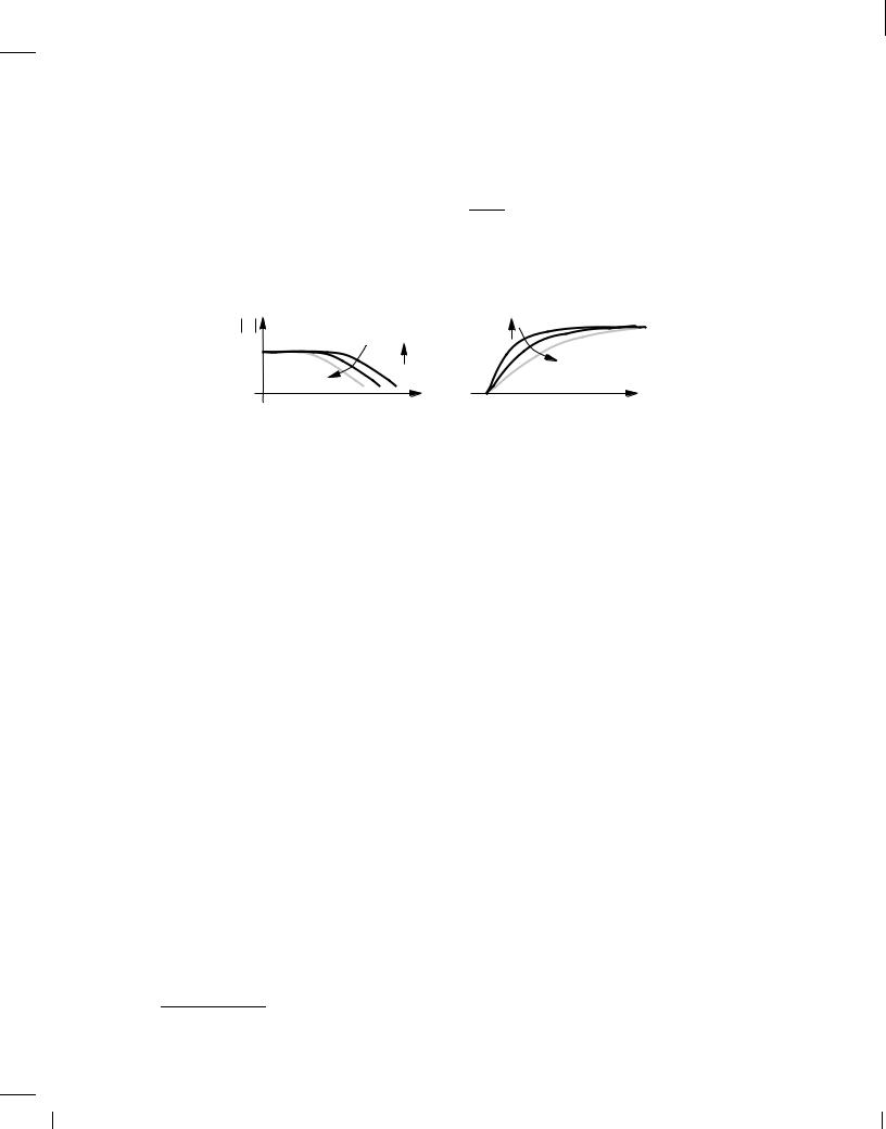
The general expression in Eq. (11.22) can be interpreted as follows: an impedance tied between the input and output of an inverting amplifier with a gain of Av is lowered by a factor of 1 + Av if seen at the input (with respect to ground). This reduction of impedance (hence increase in capacitance) is called “Miller effect.” For example, we say Miller effect raises the input capacitance of the circuit in Fig. 11.15(a) to (1 + gmRD)CF .
11.1.6 General Frequency Response
Our foregoing study indicates that capacitances in a circuit tend to lower the voltage gain at high frequencies. It is possible that capacitors reduce the gain at low frequencies as well. As a simple example, consider the high-pass filter shown in Fig. 11.16(a), where the voltage division between C1 and R1 yields
|
Vout |
C1 |
Vin |
|
1.0 |
v in |
R1 Vout |
1 |
ω |
R 1C1
(a) |
(b) |
Figure 11.16 (a) Simple high-pass filter, and (b) its frequency response.
Vout (s) = |
R |
|
|
|
|
|
||||||
|
|
|
|
|
|
1 |
|
|
|
|
|
|
Vin |
|
|
|
|
|
|
|
1 |
|
|
|
|
|
|
|
|
|
R1 + C1s |
|
|
|||||
|
|
= |
|
R1C1s |
; |
|
||||||
|
|
R1C1s + 1 |
||||||||||
|
|
|
|
|
|
|
||||||
and hence |
|
|
|
|
|
|
|
|
|
|
|
|
Vout |
= |
|
|
|
R |
C |
! |
|
|
: |
||
|
|
|
|
|
1 |
1 |
|
|
|
|
|
|
|
|
|
|
|
|
|
|
|
|
|
|
|
|
|
|
|
|
2 |
2 |
|
2 |
|
|
|
|
Vin |
|
|
pR1C1 !1 + 1 |
|||||||||
(11.36)
(11.37)
(11.38)
BR |
Wiley/Razavi/Fundamentals of Microelectronics [Razavi.cls v. 2006] |
June 30, 2007 at 13:42 |
550 (1) |
|
|
|
|
550 |
Chap. 11 |
Frequency Response |
Plotted in Fig. 11.16(b), the response exhibits a roll-off as the frequency of operation falls below 1=(R1C1). As seen from Eq. (11.37), this roll-off arises because the zero of the transfer function occurs at the origin.
The low-frequency roll-off may prove undesirable. The following example illustrates this point.
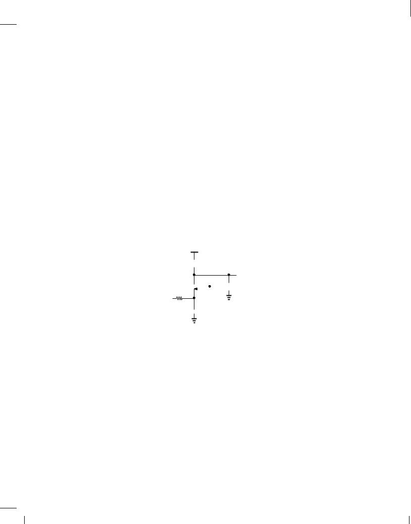
Example 11.11
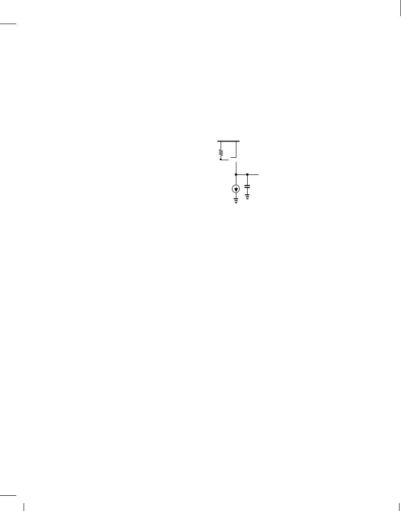
Figure 11.17 depicts a source follower used in a high-quality audio amplifier. Here, Ri estab-
R i
Vin


Ci
VDD


 M 1
M 1
 Vout
Vout
I 1 |
CL |
Figure 11.17
lishes a gate bias voltage equal to VDD for M1, and I1 defines the drain bias current. Assume= 0; gm = 1=(200 ), and R1 = 100 k . Determine the minimum required value of C1 and the maximum tolerable value of CL.
Solution
Similar to the high-pass filter of Fig. 11.16, the input network consisting of Ri and Ci attenuates the signal at low frequencies. To ensure that audio components as low as 20 Hz experience a small attenuation, we set the corner frequency 1=(RiCi) to 2 (20 Hz), thus obtaining
Ci = 79:6 nF: |
(11.39) |
This value is, of course, much to large to be integrated on a chip. Since Eq. (11.38) reveals a 3-dB attenuation at ! = 1=(RiCi), in practice we must choose even a larger capacitor if a lower attenuation is desired.
The load capacitance creates a pole at the output node, lowering the gain at high frequencies. Setting the pole frequency to the upper end of the audio range, 20 kHz, and recognizing that the resistance seen from the output node to ground is equal to 1=gm, we have
!p;out = gm |
(11.40) |
CL |
|
= 2 (20 kHz); |
(11.41) |
and hence |
|
CL = 39:8 nF: |
(11.42) |
An efficient driver, the source follower can tolerate a very large load capacitance (for the audio band).
Exercise
Repeat the above example if I1 and the width of M1 are halved.