

Fundamentals of Microelectronics
.pdfBR |
Wiley/Razavi/Fundamentals of Microelectronics [Razavi.cls v. 2006] |
June 30, 2007 at 13:42 |
531 (1) |
|
|
|
|
Sec. 10.7 |
Chapter Summary |
531 |
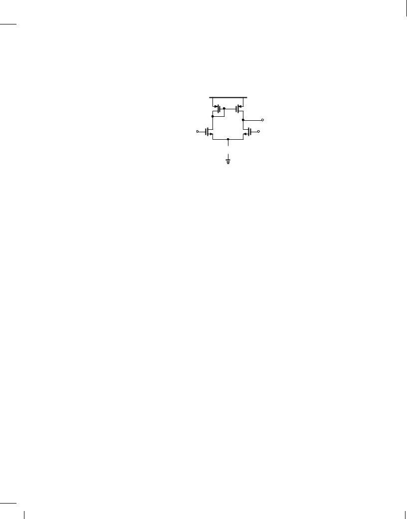
VDD
M 3 


 M 4
M 4
I 1 |
Vout |
RL |
Figure 10.90
VDD
M 3 


 M 4
M 4
 Vout
Vout
I 1 |
I 2 |
RL |
Figure 10.91 |
|
VDD |
|
M 3 |
M 4 |
|
N |
Y |
|
M 1 |
M 2 |
v CM |
|
P |
|
|
|
|
I SS |
|
Figure 10.92
(c) What happens to the results obtained in (a) and (b) if VDD changes by a small amount
V ?
74.Neglecting channel-length modulation, compute the small-signal gains vout=i1 and vout=i2 in Fig. 10.93.
VDD
M 3 


 M 4
M 4
 Vout
Vout
I 1 |
I 2 |
RL |
Figure 10.93
75.We wish to design the stage shown in Fig. 10.94 for a voltage gain of 100. If VA;n = 5 V, what is the required Early voltage for the pnp transistors?
76.Repeat the analysis in Fig. 10.56 but by constructing a Norton equivalent for the input differential pair.
77.Determine the output impedance of the circuit shown in Fig. 10.54. Assume gmrO 1.
BR |
Wiley/Razavi/Fundamentals of Microelectronics [Razavi.cls v. 2006] |
June 30, 2007 at 13:42 |
532 (1) |
|
|
|
|
532 |
|
|
Chap. 10 |
Differential Amplifiers |
|
|
|
VCC |
|
|
Q 3 |
|
Q 4 |
|
|
|
|
Vout |
|
Vin1 |
Q 1 |
Q 2 |
Vin2 |
|
 I EE
I EE
Figure 10.94
78.Using the result obtained in Problem 77 and the relationship Av = ,GmRout, compute the voltage gain of the stage.
Design Problems
79.Design the bipolar differential pair of Fig. 10.6(a) for a voltage gain of 10 and a power budget of 2 mW. Assume VCC = 2:5 V and VA = 1.
80.The bipolar differential pair of Fig. 10.6(a) must operate with an input common-mode level of 1.2 V without driving the transistors into saturation. Design the circuit for maximum voltage gain and a power budget of 3 mW. Assume VCC = 2:5 V.
81.The differential pair depicted in Fig. 10.95 must provide a gain of 5 and a power budget of 4
|
|
|
VCC |
|
R C |
|
RC |
|
|
Vout |
|
Vin1 |
Q 1 |
Q 2 |
Vin2 |
|
I EE |
R E |
I EE |
|
|
Figure 10.95
mW. Moreover, the gain of the circuit must change by less than 2% if the collector current of either transistor changes by 10%. Assuming VCC = 2:5 V and VA = 1, design the circuit. (Hint: a 10% change in IC leads to a 10% change in gm.)
82. Design the circuit of Fig. 10.96 for a gain of 50 and a power budget of 1 mW. Assume
|
|
|
VCC |
Vb |
Q 3 |
|
Q 4 |
|
Vout |
|
|
|
|
|
|
Vin1 |
Q 1 |
Q 2 |
Vin2 |
 I EE
I EE
Figure 10.96
VA;n = 6 V and VCC = 2:5 V.
83. Design the circuit of Fig. 10.97 for a gain of 100 and a power budget of 1 mW. Assume
BR |
Wiley/Razavi/Fundamentals of Microelectronics [Razavi.cls v. 2006] |
June 30, 2007 at 13:42 |
533 (1) |
|
|
|
|
Sec. 10.7 Chapter Summary |
|
|
533 |
|
|
|
VCC |
|
Q 3 |
|
Q 4 |
|
R1 |
R 2 |
|
|
Vout |
|
|
Vin1 |
Q 1 |
Q 2 |
Vin2 |
|
P |
I EE |
|
|
|
|
Figure 10.97
VA;n = 10 V, VA;p = 5 V, and VCC = 2:5 V. Also, R1 = R2.
84.Design the MOS differential pair of Fig. 10.29 for Vin;max = 0:3 V and a power budget of 3 mW. Assume RD = 500 , = 0, nCox = 100 A=V2, and VDD = 1:8 V.
85.Design the MOS differential pair of Fig. 10.29 for an equilibrium overdrive voltage of 100
mV and a power budget of 2 mW. Select the value of RD to place the transistor at the edge of triode region for an input common-mode level of 1 V. Assume = 0, nCox = 100 A=V2, VT H;n = 0:5 V, and VDD = 1:8 V. What is the voltage gain of the resulting design?
86.Design the MOS differential pair of Fig. 10.29 for a voltage gain of 5 and a power dissipation
of 1 mW if the equilibrium overdrive must be at least 150 mV. Assume = 0, nCox = 100 A=V2, and VDD = 1:8 V.
87.The differential pair depicted in Fig. 10.98 must provide a gain of 40. Assuming the same
VDD
Vb1 


 M 4
M 4
M 3
Vout
Vin1 |
M 1 M 2 |
Vin2 |
Vb2 

 M 5
M 5
Figure 10.98
(equilibrium) overdrive for all of the transistors and a power dissipation of 2 mW, design the circuit. Assume n = 0:1 V,1, p = 0:2 V,1, nCox = 100 A=V2, pCox =
100 A=V2, and VDD = 1:8 V.
88.Design the circuit of Fig. 10.37(a) for a voltage gain of 4000. Assume Q1-Q4 are identical and determine the required Early voltage. Also, = 100, VCC = 2:5 V, and the power budget is 1 mW.
89.Design the telescopic cascode of Fig. 10.38(a) for a voltage gain of 2000. Assume Q1-Q4 are identical and so are Q5-Q8. Also, n = 100, p = 50, VA;n = 5 V, VCC = 2:5 V, and the power budget is 2 mW.
90.Design the telescopic cascode of Fig. 10.41(a) for a voltage gain of 600 and a power budget
of 4 mW. Assume an (equilibrium) overdrive of 100 mV for the NMOS devices and 150 mV for the PMOS devices. If VDD = 1.8 V, nCox = 100 A=V2, pCox = 50 A=V2, and
BR |
Wiley/Razavi/Fundamentals of Microelectronics [Razavi.cls v. 2006] |
June 30, 2007 at 13:42 |
534 (1) |
|
|
|
|
534 Chap. 10 Differential Amplifiers
n = 0:1 V,1, determine the required value of p. Assume M1-M4 are identical and so are
M5-M8.
91. The differential pair of Fig. 10.99 must achieve a CMRR of 60 dB (= 100). Assume a power
|
VDD |
|
R D |
RD + |
RD |
v out1 |
v out2 |
|
Vin1 |
M 1 M 2 |
Vin2 |
|
P |
|
Vb1 |
M 3 |
|
Figure 10.99
budget of 2 mW, a nominal differential voltage gain of 5, and neglecting channel-length
modulation in M1 and M2, compute the minimum required for M3. Assume (W=L)1;2 = 10=0:18, nCox = 100 A=V2, VDD = 1:8 V, and R=R = 2%.
92.Design the differential pair of Fig. 10.48 for a voltage gain of 200 and a power budget of 3 mW with a 2.5-V supply. Assume VA;n = 2VA;p.
93.Design the circuit of Fig. 10.54 for a voltage gain of 20 and a power budget of 1 mW with
VDD = 1:8 V. Assume M1 operates at the edge of saturation if the input common-mode level is 1 V. Also, nCox = 2 pCox = 100 A=V2, VT H;n = 0:5 V, VT H;p = ,0:4 V,
n = 0:5 p = 0:1 V,1.
SPICE Problems
In the following problems, use the MOS device models given in the Appendix I. For bipolar transistors, assume IS;npn = 5 10,16 A, npn = 100, VA;npn = 5 V, IS;pnp = 8 10,16
A, pnp = 50, VA;pnp = 3:5 V.
94.Consider the differential amplifier shown in Fig. 10.100, where the input CM level is equal to 1.2 V.
|
|
|
VCC = 2.5 V |
Vb |
|
|
Q 4 |
|
|
Vout |
|
Vin1 |
Q 1 |
Q 2 |
Vin2 |
1 mA I EE
I EE
Figure 10.100
(a)Adjust the value of Vb so as to set the output CM level to 1.5 V.
(b)Determine the small-signal differential gain of the circuit. (Hint: to provide differential inputs, use an independent voltage source for one side and a voltage-dependent voltage source for the other.)
(c)What happens to the output CM level and the gain if Vb varies by 10 mV?
95.The differential amplifier depicted in Fig. 10.101 employs two current mirrors to establish the bias for the input and load devices. Assume W=L = 10 m=0:18 m for M1-M6. The input CM level is equal to 1.2 V.
BR |
Wiley/Razavi/Fundamentals of Microelectronics [Razavi.cls v. 2006] |
June 30, 2007 at 13:42 |
535 (1) |
|
|
|
|
Sec. 10.7 Chapter Summary |
|
|
|
535 |
|
|
|
|
VDD = 1.8 V |
M 7 |
|
M 3 |
|
M 4 |
|
|
Vout |
|
|
|
|
|
|
|
1 kΩ |
Vin1 |
|
M 1 M 2 |
Vin2 |
M 6 |
|
|
M 5 |
|
Figure 10.101 |
|
|
|
|
(a)Select (W=L)7 so as to set the output CM level to 1.5 V. (Assume L7 = 0:18 m.)
(b)Determine the small-signal differential gain of the circuit.
(c)Plot the differential input/output characteristic.
96.Consider the circuit illustrated in Fig. 10.102. Assume a small dc drop across R1 and R2.
|
|
|
VCC = 2.5 V |
|
Q 3 |
|
Q 4 |
|
R1 |
R 2 |
|
|
Vout |
|
|
Vin1 |
Q 1 |
Q 2 |
Vin2 |
1 mA I EE
I EE
Figure 10.102
(a)Select the input CM level to place Q1 and Q2 at the edge of saturation.
(b)Select the value of R1 (= R2) such that these resistors reduce the differential gain by no more than 20%.
97.In the differential amplifier of Fig. 10.103, Assume an input CM level of 1 V and Vb
W=L = 10 m=0:18 m for all of the transistors.
= 1:5 V.
|
M 7 |
M 8 |
VDD = 1.8 V |
|
|
||
M 9 |
|
|
|
I 1 |
M 3 |
|
|
|
Vout |
|
|
Vb |
|
|
M 4 |
Vin1 |
M 1 |
M 2 |
Vin2 |
1 mA  I SS
I SS
Figure 10.103
(a) Select the value of I1 so that the output CM level places M3 and M4 at the edge of saturation.
BR |
Wiley/Razavi/Fundamentals of Microelectronics [Razavi.cls v. 2006] |
June 30, 2007 at 13:42 |
536 (1) |
|
|
|
|
536 |
Chap. 10 |
Differential Amplifiers |
(b) Determine the small-signal differential gain.
98.In the circuit of Fig. 10.104, W=L = 10 m=0:18 m for M1-M4. Assume an input CM level of 1.2 V.
|
|
VDD = 1.8 V |
M 3 |
|
M 4 |
X |
|
Vout |
Vin1 |
M 1 M 2 |
Vin2 |
0.5 mA  I SS
I SS
Figure 10.104
(a)Determine the output dc level and explain why it is equal to VX /
(b)Determine the small-signal gains vout=(vin1 , vin2) and vX =(vin1 , vin2).
(c)Determine the change in the output dc level if W4 changes by 5%.
References
1. B. Razavi, Design of Analog CMOS Integrated Circuits McGraw-Hill, 2001.
BR |
Wiley/Razavi/Fundamentals of Microelectronics [Razavi.cls v. 2006] |
June 30, 2007 at 13:42 |
537 (1) |
|
|
|
|
Frequency Response
The need for operating circuits at increasingly higher speeds has always challenged designers. From radar and television systems in the 1940s to gigahertz microprocessors today, the demand for pushing circuits to higher frequencies has required a solid understanding of their speed limitations.
In this chapter, we study the effects that limit the speed of transistors and circuits, identifying topologies that better lend themselves to high-frequency operation. We also develop skills for deriving transfer functions of circuits, a critical task in the study of stability and frequency compensation (12). We assume bipolar transistors remain in the active mode and MOSFETs in the saturation region. The outline is shown below.
Fundamental |
High−Frequency |
Frequency |
Concepts |
Models of Transistors |
Response of Circuits |
Bode's Rules |
Bipolar Model |
CE/CS Stages |
Association of Poles |
MOS Model |
CB/CG Stages |
with Nodes |
Transit Frequency |
Followers |
Miller's Theorem |
|
Cascode Stage |
|
|
Differential Pair |
11.1 Fundamental Concepts
11.1.1 General Considerations
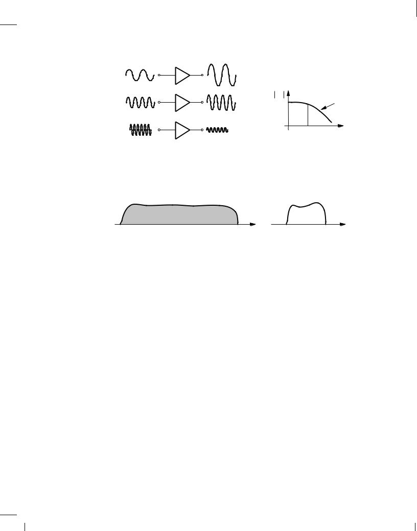
What do we mean by “frequency response?” Illustrated in Fig. 11.1(a), the idea is to apply a sinusoid at the input of the circuit and observe the output while the input frequency is varied. As exemplified by Fig. 11.1(a), the circuit may exhibit a high gain at low frequencies but a “roll-off” as the frequency increases. We plot the magnitude of the gain as in Fig. 11.1(b) to represent the circuit's behavior at all frequencies of interest. We may loosely call f1 the useful bandwidth of the circuit. Before investigating the cause of this roll-off, we must ask: why is frequency response important? The following examples illustrate the issue.
Example 11.1
Explain why people's voice over the phone sounds different from their voice in face-to-face conversation.
537
BR |
Wiley/Razavi/Fundamentals of Microelectronics [Razavi.cls v. 2006] |
June 30, 2007 at 13:42 |
538 (1) |
|
|
|
|
538 |
Chap. 11 |
Frequency Response |
A v |
Roll−Off |
f1 f
(a) |
(b) |
Figure 11.1 (a) Conceptual test of frequency response, (b) gain roll-off with frequency.
Solution
Human voice contains frequency components from 20 Hz to 20 kHz [Fig. 11.2(a)]. Thus, circuits
20 Hz |
20 kHz f |
400 Hz |
3.5 kHz f |
(a) |
|
|
(b) |
Figure 11.2
processing the voice must accommodate this frequency range. Unfortunately, the phone system suffers from a limited bandwidth, exhibiting the frequency response shown in Fig. 11.2(b). Since the phone suppresses frequencies above 3.5 kHz, each person's voice is altered. In high-quality audio systems, on the other hand, the circuits are designed to cover the entire frequency range.
Exercise
Whose voice does the phone system alter more, men's or women's?
Example 11.2
When you record your voice and listen to it, it sounds somewhat different from the way you hear it directly when you speak. Explain why?
Solution
During recording, your voice propagates through the air and reaches the audio recorder. On the other hand, when you speak and listen to your own voice simultaneously, your voice propagates not only through the air but also from your mouth through your skull to your ear. Since the frequency response of the path through your skull is different from that through the air (i.e., your skull passes some frequencies more easily than others), the way you hear your own voice is different from the way other people hear your voice.
Exercise
Explain what happens to your voice when you have a cold?
BR |
Wiley/Razavi/Fundamentals of Microelectronics [Razavi.cls v. 2006] |
June 30, 2007 at 13:42 |
539 (1) |
|
|
|
|
Sec. 11.1 |
Fundamental Concepts |
539 |
Example 11.3
Video signals typically occupy a bandwidth of about 5 MHz. For example, the graphics card delivering the video signal to the display of a computer must provide at least 5 MHz of bandwidth. Explain what happens if the bandwidth of a video system is insufficient.
Solution
With insufficient bandwidth, the “sharp” edges on a display become “soft,” yielding a fuzzy picture. This is because the circuit driving the display is not fast enough to abruptly change the contrast from, e.g., complete white to complete black from one pixel to the next. Figures 11.3(a) and (b) illustrate this effect for a high-bandwidth and low-bandwidth driver, respectively. (The display is scanned from left to right.)
|
|
|
|
|
|
|
|
|
|
|
|
|
|
|
|
|
|
|
|
|
|
|
|
|
|
|
|
|
|
|
(a) |
|
(b) |
|
Figure 11.3
Exercise
What happens if the display is scanned from top to bottom?
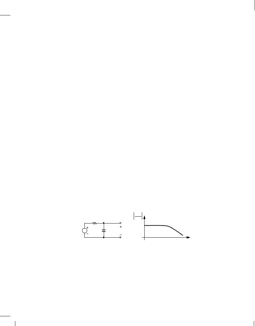
What causes the gain roll-off in Fig. 11.1? As a simple example, let us consider the low-pass filter depicted in Fig. 11.4(a). At low frequencies, C1 is nearly open and the current through R1
|
Vout |
R1 |
Vin |
Vin |
1.0 |
C1 Vout |
f
Figure 11.4 (a) Simple low-pass filter, and (b) its frequency response.
nearly zero; thus, Vout = Vin. As the frequency increases, the impedance of C1 falls and the voltage divider consisting of R1 and C1 attenuates Vin to a greater extent. The circuit therefore exhibits the behavior shown in Fig. 11.4(b).
As a more interesting example, consider the common-source stage illustrated in Fig. 11.5(a), where a load capacitance, CL, appears at the output. At low frequencies, the signal current produced by M1 prefers to flow through RD because the impedance of CL, 1=(CLs), remains high. At high frequencies, on the other hand, CL “steals” some of the signal current and shunts it to ground, leading to a lower voltage swing at the output. In fact, from the small-signal equivalent
BR |
Wiley/Razavi/Fundamentals of Microelectronics [Razavi.cls v. 2006] |
June 30, 2007 at 13:42 |
540 (1) |
|
|
|
|
540 |
|
|
Chap. 11 |
Frequency Response |
|
|
|
VDD |
|
|
|
|
R D |
Vin |
|
|
Vout |
|
|
Vout |
gmVin |
RD |
CL |
Vin |
|
M 1 CL |
|||
|
|
|
|
||
|
|
(a) |
(b) |
|
|
Figure 11.5 (a) CS stage with load capacitance, (b) small-signal model of the circuit.
circuit of Fig. 11.5(b),1 we note that RD and CL are in parallel and hence:
V |
= ,g |
V |
|
(R jj |
1 |
): |
(11.1) |
|
|
||||||
out |
m |
|
in |
D |
CLs |
|
|
That is, as the frequency increases, the parallel impedance falls and so does the amplitude of Vout.2 The voltage gain therefore drops at high frequencies.
The reader may wonder why we use sinusoidal inputs in our study of frequency response. After all, an amplifier may sense a voice or video signal that bears no resemblance to sinusoids. Fortunately, such signals can be viewed as a summation of many sinusoids with different frequencies (and phases). Thus, responses such as that in Fig. 11.5(b) prove useful so long as the circuit remains linear and hence superposition can be applied.
11.1.2 Relationship Between Transfer Function and Frequency Response
We know from basic circuit theory that the transfer function of a circuit can be written as
|
1 + |
s |
1 + |
s |
|
|
|
H(s) = A0 |
|
|
; |
|
|||
!z1 |
!z2 |
(11.2) |
|||||
|
|
||||||
|
1 + |
s |
1 + |
s |
|
|
|
|
!p1 |
!p2 |
|
||||
where A0 denotes the low frequency gain because H(s) ! A0 as s ! 0. The frequencies !zj and !pj represent the zeros and poles of the transfer function, respectively. If the input to the circuit is a sinusoid of the form x(t) = A cos(2 ft) = A cos !t, then the output can be expressed as
y(t) = AjH(j!)j cos [!t + 6 |
H(j!)] ; |
(11.3) |
|
|
|
|
|
where H(j!) is obtained by making the substitution s = j!. Called the “magnitude” and the “phase,” jH(j!)j and 6 H(j!) respectively reveal the frequency response of the circuit. In this chapter, we are primarily concerned with the former. Note that f (in Hz) and ! (in radians per second) are related by a factor of 2 . For example, we may write ! = 5 1010 rad/s
= 2 (7:96 GHz):
Example 11.4
Determine the transfer function and frequency response of the CS stage shown in Fig. 11.5(a).
1Channel-length modulation is neglected here.
2We use upper case letters for frequency-domain quantities (Laplace transforms) even though they denote smallsignal values.