


CY7C68013
10.0Ordering Information
Table 10-1. Ordering Information
Ordering Code |
Package Type |
RAM Size |
# Prog I/Os |
8051 Address/Data Buses |
|
|
|
|
|
CY7C68013-128AC |
128 TQFP |
8K |
40 |
16/8 bit |
|
|
|
|
|
CY7C68013-100AC |
100 TQFP |
8K |
40 |
– |
|
|
|
|
|
CY7C68013-56PVC |
56 SSOP |
8K |
24 |
– |
|
|
|
|
|
CY7C68013-56LFC |
56 QFN |
8K |
24 |
– |
|
|
|
|
|
CY7C68013-128AXC |
128 TQFP Lead-Free Package |
8K |
40 |
16/8 bit |
|
|
|
|
|
CY7C68013-100AXC |
100 TQFP Lead-Free Package |
8K |
40 |
– |
|
|
|
|
|
CY7C68013-56PVXC |
56 SSOP Lead-Free Package |
8K |
24 |
– |
|
|
|
|
|
CY7C68013-56LFXC |
56 QFN Lead-Free Package |
8K |
24 |
– |
|
|
|
|
|
CY3681 |
EZ-USB FX2 Xcelerator Development Kit |
|
|
|
|
|
|
|
|
Document #: 38-08012 Rev. *F |
Page 44 of 48 |

CY7C68013
11.0Package Diagrams
The FX2 is available in four packages:
•56-pin SSOP
•56-pin QFN
•100-pin TQFP
•128-pin TQFP.
51-85062-*C
Figure 11-1. 56-lead Shrunk Small Outline Package O56
|
TOP VIEW |
SIDE VIEW |
|
|
|
0.08[0.003] |
C |
|
7.90[0.311] |
1.00[0.039] MAX. |
|
A |
|
|
|
8.10[0.319] |
0.05[0.002] MAX. |
|
|
|
|
||
|
7.70[0.303] |
0.80[0.031] MAX. |
|
|
|
|
|
|
7.80[0.307] |
0.20[0.008] REF. |
|
|
N |
|
|
1
0.80[0.031] 2
DIA.
7.70[0.303] |
7.80[0.307] |
7.90[0.311] |
8.10[0.319] |
0.30[0.012]
0.50[0.020]
0°-12°
C
SEATING
PLANE
BOTTOM VIEW
0.18[0.007]
0.28[0.011]
NPIN1 ID 0.20[0.008] R.
1 |
|
2 |
0.45[0.018] |
|
E-PAD
(PAD SIZE VARY |
|
6.45[0.254] |
6.55[0.258] |
BY DEVICE TYPE) |
|
|
|
|
0.24[0.009] |
(4X) |
|
|
0.60[0.024] |
|
|
|
0.50[0.020] |
|
|
6.45[0.254] |
|
|
|
6.55[0.258] |
|
|
|
51-85144-*D
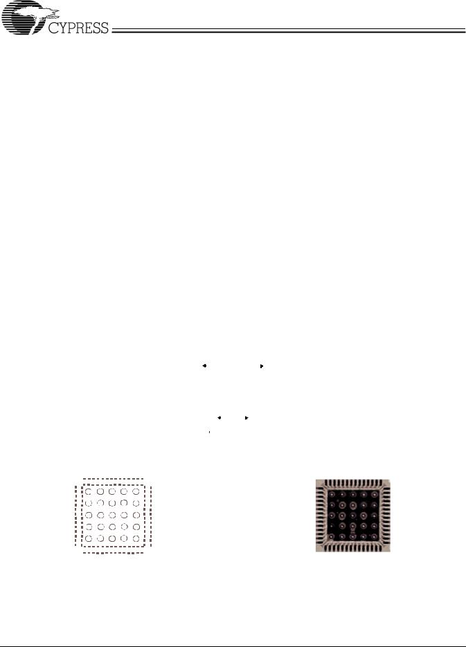
Figure 11-2. 56-Lead QFN 8 x 8 MM LF56A
Document #: 38-08012 Rev. *F |
Page 45 of 48 |

CY7C68013
 51-85050
 -*A
-*A
Figure 11-3. 100-Pin Thin Plastic Quad Flatpack (14 x 20 x 1.4 mm) A101
51-85101-*B
Figure 11-4. 128-Lead Thin Plastic Quad Flatpack (14 x 20 x 1.4 mm) A128
Document #: 38-08012 Rev. *F |
Page 46 of 48 |
CY7C68013
12.0PCB Layout Recommendations[17]
The following recommendations should be followed to ensure reliable high-performance operation.
•At least a four-layer impedance controlled boards are required to maintain signal quality.
•Specify impedance targets (ask your board vendor what they can achieve).
•To control impedance, maintain trace widths and trace spacing.
•Minimize stubs to minimize reflected signals.
•Connections between the USB connector shell and signal ground must be done near the USB connector.
•Bypass/flyback caps on VBus, near connector, are recommended.
•DPLUS and DMINUS trace lengths should be kept to within two mm of each other in length, with preferred length of 2030 mm.
•Maintain a solid ground plane under the DPLUS and DMINUS traces. Do not allow the plane to be split under these traces.
•It is preferred is to have no vias placed on the DPLUS or DMINUS trace routing.
•Isolate the DPLUS and DMINUS traces from all other signal traces by no less than 10 mm.
13.0 Quad Flat Package No Leads (QFN)
Package Design Notes
Electrical contact of the part to the Printed Circuit Board (PCB) is made by soldering the leads on the bottom surface of the package to the PCB. Hence, special attention is required to the heat transfer area below the package to provide a good
thermal bond to the circuit board. A Copper (Cu) fill is to be designed into the PCB as a thermal pad under the package. Heat is transferred from the FX2 through the device’s metal paddle on the bottom side of the package. Heat from here, is conducted to the PCB at the thermal pad. It is then conducted from the thermal pad to the PCB inner ground plane by a 5 x 5 array of via. A via is a plated through hole in the PCB with a finished diameter of 13 mil. The QFN’s metal die paddle must be soldered to the PCB’s thermal pad. Solder mask is placed on the board top side over each via to resist solder flow into the via. The mask on the top side also minimizes outgassing during the solder reflow process.
For further information on this package design please refer to the application note “Surface Mount Assembly of AMKOR’s MicroLeadFrame (MLF) Technology.” This application note can be downloaded from AMKOR’s website from the following URL:
“www.amkor.com/products/notes_papers/MLF_AppNote_090 2.pdf”. The application note provides detailed information on board mounting guidelines, soldering flow, rework process, etc.
Figure 13-1 below display a cross-sectional area underneath the package. The cross section is of only one via. The solder paste template needs to be designed to allow at least 50% solder coverage. The thickness of the solder paste template should be 5 mil. It is recommended that “No Clean”, type 3 solder paste is used for mounting the part. Nitrogen purge is recommended during reflow.
Figure 13-2 is a plot of the solder mask pattern and Figure 13- 3 displays an X-Ray image of the assembly (darker areas indicate solder.).
|
|
|
|
|
|
0.017” dia |
|
|
|
|
|
|
||
|
|
|
|
|
|
|
|
|
|
|
|
|||
|
|
|
|
|
|
|
|
|
|
|
|
|
|
|
|
|
|
|
|
|
|
|
|
|
|
|
|
|
|
|
|
|
|
Solder Mask |
|
|
|
|
|
|||||
|
Cu Fill |
|
|
|
|
|
|
|
|
|
|
Cu Fill |
|
|
|
|
|
|
0.013” dia |
|
|
|
|
|
|||||
PCB Material |
|
|
|
PCB Material |
|
|||||||||
|
|
|
|
|
|
|
|
|
|
|||||
|
|
|
|
|
|
|
|
|
|
|
|
|
|
|
|
|
|
|
|
|
|
|
|
|
|
|
|
|
|
Via hole for thermally connecting the |
|
|
|
|
|
|
|
This figure only shows the top three layers of the circuit board: |
||||||
QFN to the circuit board ground plane. |
|
|
|
|
|
|
|
Top Solder, PCB Dielectric, and the Ground Plane |
||||||
Figure 13-1. Cross-section of the Area Underneath the QFN Package
|
|
|
|
|
|
|
|
|
|
|
|
|
|
|
|
|
|
|
Figure 13-3. X-ray Image of the Assembly |
|
|
|
|
|
|
|
|
|
|
|
|
|
|
|
|
|
|
|
|
|
|
|
|
|
|
|
|
|
|
|
|
|
|
|
|
|
|
|
|
Figure 13-2. Plot of the Solder Mask (White Area) |
|||||||||||||||||||
Note:
17.Source for recommendations: EZ-USB FX2™PCB Design Recommendations, http:///www.cypress.com/cfuploads/support/app_notes/FX2_PCB.pdf and High Speed USB Platform Design Guidelines, http://www.usb.org/developers/data/hs_usb_pdg_r1_0.pdf.
Purchase of I2C components from Cypress, or one of its sublicensed Associated Companies, conveys a license under the Philips I2C Patent Rights to use these components in an I2C system, provided that the system conforms to the I2C Standard Specification as defined by Philips. EZ-USB FX2 and ReNumeration are trademarks, and EZ-USB is a registered trademark, of Cypress Semiconductor. All product and company names mentioned in this document are the trademarks of their respective holders.
Document #: 38-08012 Rev. *F |
Page 47 of 48 |
© Cypress Semiconductor Corporation, 2005. The information contained herein is subject to change without notice. Cypress Semiconductor Corporation assumes no responsibility for the use of any circuitry other than circuitry embodied in a Cypress product. Nor does it convey or imply any license under patent or other rights. Cypress products are not warranted nor intended to be used for medical, life support, life saving, critical control or safety applications, unless pursuant to an express written agreement with Cypress. Furthermore, Cypress does not authorize its products for use as critical components in life-support systems where a malfunction or failure may reasonably be expected to result in significant injury to the user. The inclusion of Cypress

CY7C68013
Document History Page
Document Title: CY7C68013 EZ-USB FX2™ USB Microcontroller High-speed USB Peripheral Controller Document Number: 38-08012
|
|
|
Orig. of |
|
REV. |
ECN NO. |
Issue Date |
Change |
Description of Change |
|
|
|
|
|
** |
111753 |
11/15/01 |
DSG |
Changed from Spec number: 38-00929 to 38-08012 |
|
|
|
|
|
*A |
111802 |
02/20/02 |
KKU |
Updated functional changes between revision D part and revision E part |
|
|
|
|
Changed timing data from simulation data to revision E characterization data |
|
|
|
|
|
*B |
115480 |
06/26/02 |
KKU |
Added new 56-pin Quad Flatpack No Lead package and pinout |
|
|
|
|
Revised pin description table to reflect new package |
|
|
|
|
Corrected Figure 9-8 by moving tsfd parameter location |
|
|
|
|
Corrected labels on Dplus and Dminus in Table 4-1 |
|
|
|
|
Removed Preliminary from spec title |
|
|
|
|
|
*C |
120776 |
01/06/03 |
KKU |
Added bus powered references and PCB layout recommendations and QFN |
|
|
|
|
package design notes |
|
|
|
|
Updated QFN package drawing 51-85144 to current revision |
|
|
|
|
|
*D |
288810 |
See ECN |
MON |
Added lead-free packages |
|
|
|
|
Added timing sequence diagrams for slave FIFO read and write |
|
|
|
|
Changed PKTEND to FLAGS output propagation delay (asynchronous |
|
|
|
|
interface) in Table 9-13from a max value of 70 ns to 115 ns |
|
|
|
|
Changed FIFOADR[2:0] Hold Time (tFAH) for Asynchronous FIFO Interface as |
|
|
|
|
follows: |
|
|
|
|
SLRD/PKTEND to FIFOADR[2:0] Hold Time: 20 ns |
|
|
|
|
SLWR to FIFOADR[2:0] Hold Time: 70 ns |
|
|
|
|
|
*E |
317674 |
See ECN |
MON |
Provided additional timing restrictions and requirement regarding the use of |
|
|
|
|
PKTEND pin to commit a short one byte/word packet subsequent to committing |
|
|
|
|
a packet automatically (when in auto mode). |
|
|
|
|
|
*F |
352234 |
See ECN |
MON |
Added information on the AUTOPTR1/AUTOPTR2 address timing with |
|
|
|
|
regards to data memory read/write timing diagram. |
|
|
|
|
Added information “This part is not recommended for new designs. Use EZ- |
|
|
|
|
USB FX2LP instead of EZ-USB FX2 for new designs” |
|
|
|
|
|
Document #: 38-08012 Rev. *F |
Page 48 of 48 |