

CY7C68013
9.16Sequence Diagram
9.16.1Single and Burst Synchronous Read Example
tIFCLK
IFCLK |
|
|
|
|
|
|
|
|
|
|
|
|
|
|
|
|
|
|
|
|
|
|
|
|
|
|
|
|
|
|
|
|
|
|
|
|
|
||
|
|
|
|
|
|
|
|
|
|
|
|
|
|
|
|
|
|
|
|
|
|
|
|
|
|
|
|
|
|
|
|
|
|
|
|
|
|
|
|
|
|
|
|
|
|
|
t |
|
|
tFAH |
|
|
|
|
|
|
|
|
tSFA |
|
|
|
|
|
|
|
|
|
|
|
|
|
|
|
|||||
|
|
|
|
|
|
|
|
|
|
|
|
|
|
|
|
|
|
|
|
|
|
|
|
|
|
|
|
|
|
|
|
||||||||
|
|
|
|
|
|
|
SFA |
|
|
|
|
|
|
|
|
|
|
|
|
|
|
|
|
|
|
|
|
|
tFAH |
|
|
|
|||||||
|
|
|
|
|
|
|
|
|
|
|
|
|
|
|
|
|
|
|
|
|
|
|
|
|
|
|
|
|
|
|
|
|
|
|
|
||||
FIFOADR |
|
|
|
|
|
|
|
|
|
|
|
|
|
|
|
|
|
|
|
|
|
|
|
|
|
|
|
|
|
|
|
|
|
||||||
|
|
|
|
|
|
|
|
|
|
|
|
|
|
|
|
|
|
|
|
|
|
|
|
|
|
|
|
|
|
|
|
|
|
|
|
|
|
|
|
|
t=0 |
|
|
tSRD |
|
tRDH |
|
|
|
|
|
|
T=0 |
|
>= tSRD |
|
|
|
|
|
|
>= tRDH |
|
|
|
||||||||||||||
|
|
|
|
|
|
|
|
|
|
|
|
|
|
|
|
|
|
|
|
|
|
|
|
|
|
||||||||||||||
|
|
|
|
|
|
|
|
|
|
|
|
|
|
|
|
|
|
|
|
|
|
|
|
|
|
|
|
|
|
|
|
|
|
|
|
|
|
|
|
SLRD
t=2 |
t=3 |
T=2 |
T=3 |
|
SLCS
FLAGS |
|
|
|
|
|
|
|
tXFLG |
|
|
|
|
|
|
|
|
|
|
|
|
|
|
|
|
|
|
|
|
|||||||
|
|
|
|
|
|
|
|
|
|
|
|
|
|
|
|
|
|
|
|
|
|
|
|
|
|
|
|
|
|
|
|
|
|
||
|
|
|
|
|
|
|
|
|
|
|
|
|
|
|
|
|
|
|
|
|
|
|
|
|
|
|
|
|
|
|
|
|
|
|
|
|
|
|
|
|
|
|
|
|
|
|
|
|
|
|
|
tXFD |
|
|
|
|
|
|
tXFD |
|
|
|
|
||||||||
|
|
|
|
|
|
tXFD |
|
|
|
|
|
|
|
|
t |
XFD |
|
|
|
|
|
||||||||||||||
|
|
|
|
|
|
|
|
|
|
|
|
|
|
|
|
||||||||||||||||||||
|
|
|
|
|
|
|
|
|
|
|
|
|
|
|
|
|
|
|
|
|
|
|
|
|
|
|
|
|
|
|
|
|
|
|
|
DATA |
|
|
|
|
Data Driven: N |
|
|
|
|
|
N+1 |
|
|
N+1 |
|
N+2 |
|
|
|
N+3 |
|
|
|
|
N+4 |
||||||||||
|
|
|
|
|
|
|
|
|
tOEon |
||||||||||||||||||||||||||
|
|
|
|
|
|
|
|
|
|
|
|
|
|
|
|
|
|
|
|
|
|
|
|
|
|
|
|
|
|
|
|
|
|
||
|
|
|
|
t |
|
|
|
|
|
|
|
t |
|
|
|
|
|
|
|
|
|
|
|
|
|
|
|
|
|
|
t |
||||
|
|
|
|
|
OEon |
|
|
|
|
|
OEoff |
|
|
|
|
|
|
|
|
|
|
|
|
|
|
|
|
|
OEoff |
|
|
||||
|
|
|
|
|
|
|
|
|
|
|
|
|
|
|
|
|
|
|
|
|
|
|
|
|
|
|
|
|
|
|
|
|
|
|
|
SLOE
t=1 |
t=4 |
T=1 |
T=4 |
|
|
|
Figure 9-16. Slave FIFO Synchronous Read Sequence and Timing Diagram
|
|
|
IFCLK |
|
IFCLK |
|
|
|
|
IFCLK |
|
|
|
|
IFCLK |
IFCLK |
IFCLK |
IFCLK |
IFCLK |
|
|
IFCLK |
|
|
IFCLK |
|
||||||||||||||||||||
|
|
|
|
|
|
|
|
|
|
|
|
|
|
|
|
|
|
|
|
|
|
|
|
|
|
|
|
|
|
|
|
|
|
|
|
|
|
|
|
|
|
|
|
|
|
|
FIFO POINTER |
|
N |
|
|
|
|
|
N |
|
|
|
|
N+1 |
|
|
|
|
N+1 |
|
|
|
|
N+1 |
|
|
|
N+2 |
|
|
|
N+3 |
|
|
N+4 |
|
|
|
N+4 |
|
|
|
N+4 |
|
|||
|
|
|
|
|
|
|
SLOE |
|
|
|
|
|
|
|
|
|
|
|
|
|
|
|
|
|||||||||||||||||||||||
FIFO DATA BUS |
|
|
|
SLOE |
|
|
|
|
|
SLRD |
|
|
|
|
SLRD |
|
|
|
|
SLOE |
|
SLRD |
|
|
|
|
|
|
|
|
SLRD |
|
|
SLOE |
|
|
|
|
||||||||
|
|
|
|
|
|
|
|
|
|
|
|
|
|
|
|
|
|
|
|
|
|
|
|
|
|
|
|
|
|
|
|
|
|
|
|
|
|
|
|
|
|
|
|
|
||
Not Driven |
|
|
|
|
Driven: N |
|
|
|
|
N+1 |
|
|
|
|
Not Driven |
|
|
|
|
N+1 |
|
|
|
|
N+2 |
|
|
N+3 |
|
|
N+4 |
|
|
|
N+4 |
|
|
Not Driven |
|
|||||||
|
|
|
|
|
|
|
|
|
|
|
|
|
|
|
|
|
|
|
|
|
|
|
||||||||||||||||||||||||
|
|
|
|
|
|
|
|
|
|
|
|
|
|
|
|
|
|
|
|
|
|
|
|
|
|
|
|
|
|
|
|
|
|
|
|
|
|
|
|
|
|
|
|
|
|
|
Figure 9-17. Slave FIFO Synchronous Sequence of Events Diagram
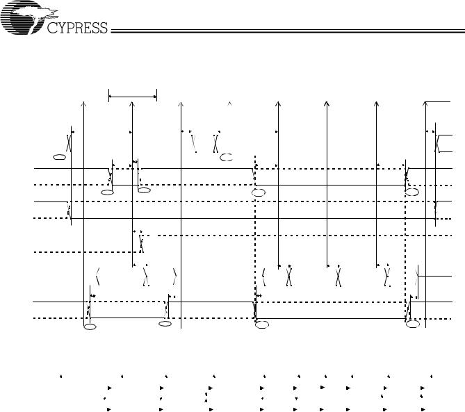
Figure 9-16 shows the timing relationship of the SLAVE FIFO signals during a synchronous FIFO read using IFCLK as the synchronizing clock. The diagram illustrates a single read followed by a burst read.
•At t = 0 the FIFO address is stable and the signal SLCS is asserted (SLCS may be tied low in some applications).
Note: tSFA has a minimum of 25 ns. This means when IFCLK is running at 48 MHz, the FIFO address set-up time is more than one IFCLK cycle.
•At = 1, SLOE is asserted. SLOE is an output enable only, whose sole function is to drive the data bus. The data that is driven on the bus is the data that the internal FIFO pointer is currently pointing to. In this example it is the first data value in the FIFO. Note: the data is pre-fetched and is driven on the bus when SLOE is asserted.
•At t = 2, SLRD is asserted. SLRD must meet the setup time
of tSRD (time from asserting the SLRD signal to the rising edge of the IFCLK) and maintain a minimum hold time of
tRDH (time from the IFCLK edge to the de-assertion of the SLRD signal). If the SLCS signal is used, it must be asserted
with SLRD, or before SLRD is asserted (i.e. the SLCS and SLRD signals must both be asserted to start a valid read condition).
•The FIFO pointer is updated on the rising edge of the IFCLK, while SLRD is asserted. This starts the propagation of data from the newly addressed location to the data bus. After a
propagation delay of tXFD (measured from the rising edge of IFCLK) the new data value is present. N is the first data value read from the FIFO. In order to have data on the FIFO data bus, SLOE MUST also be asserted.
The same sequence of events are shown for a burst read and are marked with the time indicators of T = 0 through 5. Note: For the burst mode, the SLRD and SLOE are left asserted during the entire duration of the read. In the burst read mode, when SLOE is asserted, data indexed by the FIFO pointer is on the data bus. During the first read cycle, on the rising edge of the clock the FIFO pointer is updated and increments to point to address N+1. For each subsequent rising edge of IFCLK, while the SLRD is asserted, the FIFO pointer is incremented and the next data value is placed on the data bus.
Document #: 38-08012 Rev. *F |
Page 40 of 48 |
CY7C68013
9.16.2Single and Burst Synchronous Write
tIFCLK
IFCLK |
|
|
|
|
|
|
|
|
|
|
|
|
|
|
tSFA |
t |
|
tSFA |
|
|
|
|
|
t |
FAH |
|
|
|
FAH |
|
|
|
|
|
|
|
|
|
FIFOADR |
|
|
|
|
|
|
|
|
|
|
|
|
|
t=0 |
tSWR |
t |
T=0 |
>= t |
|
|
|
|
|
>= tWRH |
|
|
|
|
WRH |
|
SWR |
|
|
|
|
|
|
|
SLWR |
|
|
|
|
|
|
|
|
|
|
|
|
|
|
t=2 |
t=3 |
|
T=2 |
|
|
|
|
|
T=5 |
|
|
|
|
|
|
|
|
|
|
|
|
||
SLCS |
|
|
|
|
|
|
|
|
|
|
|
|
|
|
|
tXFLG |
|
|
|
|
|
|
|
tXFLG |
|
|
|
|
|
|
|
|
|
|
|
|
|
|
FLAGS |
|
|
|
|
|
|
|
|
|
|
|
|
|
|
tSFD |
tFDH |
|
tSFD |
tFDH |
tSFD |
tFDH |
|
tSFD |
tFDH |
|
DATA |
|
N |
|
|
N+1 |
|
N+2 |
|
|
N+3 |
|
|
|
|
t=1 |
|
|
T=1 |
T=3 |
|
|
T=4 |
tSPE |
tPEH |
|
|
|
|
|
|
|
|
|
|
||||
|
|
|
|
|
|
|
|
|
|
|
|
|
PKTEND |
|
|
|
|
|
|
|
|
|
|
|
|
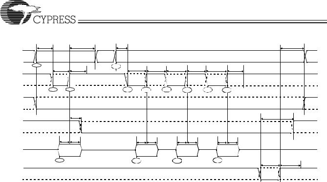
Figure 9-18. Slave FIFO Synchronous Write Sequence and Timing Diagram[13]
The Figure 9-18 shows the timing relationship of the SLAVE FIFO signals during a synchronous write using IFCLK as the synchronizing clock. The diagram illustrates a single write followed by burst write of three bytes and committing all four bytes as a short packet using the PKTEND pin.
•At t = 0 the FIFO address is stable and the signal SLCS is asserted. (SLCS may be tied low in some applications)
Note: tSFA has a minimum of 25 ns. This means when IFCLK is running at 48 MHz, the FIFO address setup time is more than one IFCLK cycle.
•At t = 1, the external master/peripheral must outputs the data value onto the data bus with a minimum set up time of tSFD before the rising edge of IFCLK.
•At t = 2, SLWR is asserted. The SLWR must meet the setup
time of tSWR (time from asserting the SLWR signal to the rising edge of IFCLK) and maintain a minimum hold time of
tWRH (time from the IFCLK edge to the deassertion of the SLWR signal). If SLCS signal is used, it must be asserted with SLWR or before SLWR is asserted. (i.e., the SLCS and SLWR signals must both be asserted to start a valid write condition).
•While the SLWR is asserted, data is written to the FIFO and on the rising edge of the IFCLK, the FIFO pointer is incremented. The FIFO flag will also be updated after a delay of
tXFLG from the rising edge of the clock.
The same sequence of events are also shown for a burst write and are marked with the time indicators of T = 0 through 5. Note: For the burst mode, SLWR and SLCS are left asserted for the entire duration of writing all the required data values. In this burst write mode, once the SLWR is asserted, the data on the FIFO data bus is written to the FIFO on every rising edge
of IFCLK. The FIFO pointer is updated on each rising edge of IFCLK. In Figure 9-18, once the four bytes are written to the FIFO, SLWR is de-asserted. The short 4-byte packet can be committed to the host by asserting the PKTEND signal.
There is no specific timing requirement that needs to be met for asserting PKTEND signal with regards to asserting the SLWR signal. PKTEND can be asserted with the last data value or thereafter. The only requirement is that the set-up time
tSPE and the hold time tPEH must be met. In the scenario of Figure 9-18, the number of data values committed includes the
last value written to the FIFO. In this example, both the data value and the PKTEND signal are clocked on the same rising edge of IFCLK. PKTEND can also be asserted in subsequent clock cycles. The FIFOADDR lines should be held constant during the PKTEND assertion.
Although there is no specific timing requirement for the PKTEND assertion, there is a specific corner case condition that needs attention while using the PKTEND to commit a one byte/word packet. Additional timing requirements exists when the FIFO is configured to operate in auto mode and it is desired to send two packets: a full packet (full defined as the number of bytes in the FIFO meeting the level set in AUTOINLEN register) committed automatically followed by a short one byte/word packet committed manually using the PKTEND pin. In this case, the external master must make sure to assert the PKTEND pin at least one clock cycle after the rising edge that caused the last byte/word to be clocked into the previous auto committed packet (the packet with the number of bytes equal to what is set in the AUTOINLEN register). Refer to Figure 9- 10 for further details on this timing.
Document #: 38-08012 Rev. *F |
Page 41 of 48 |

CY7C68013
9.16.3Sequence Diagram of a Single and Burst Asynchronous Read
|
|
|
|
|
t |
|
t |
|
|
|
|
t |
SFA |
|
|
|
|
|
|
|
|
|
tFAH |
|
|||||||
|
|
|
|
|
|
|
|
|
|
|
|
|
|
|
|
|
|
|
|
||||||||||||
|
|
|
|
|
SFA |
|
FAH |
|
|
|
|
|
|
|
|
|
|
|
|
|
|
|
|
|
|||||||
|
|
|
|
|
|
|
|
|
|
|
|
|
|
|
|
|
|
|
|
|
|
|
|
|
|
|
|
|
|
|
|
|
|
|
|
|
|
|
|
|
|
|
|
|
|
|
|
|
|
|
|
|
|
|
|
|
|
|
|
|
|
|
|
FIFOADR |
|
|
|
|
|
|
|
|
|
|
|
|
|
|
|
|
|
|
|
|
|
|
|
|
|
|
|
||||
|
|
|
|
|
|
|
|
|
|
|
|
|
|
|
|
|
|
|
|
|
|
|
|
|
|
|
|
|
|
|
|
|
|
t=0 |
|
|
tRDpwl |
|
|
|
|
|
|
|
|
|
|
|
tRDpwl |
|
tRDpwh |
|
tRDpwl |
|
tRDpwh |
|
tRDpwl tRDpwh |
|
|||||
|
|
|
|
|
|
|
|
tRDpwh |
|
|
T=0 |
|
|
|
|
|
|||||||||||||||
|
|
|
|
|
|
|
|
|
|
|
|
|
|
|
|
|
|
|
|
|
|
|
|
|
|
|
|
|
|
|
|
SLRD
t=2 |
t=3 |
T=2 |
T=3 |
T=4 |
T=5 |
T=6 |
|
|
SLCS
|
|
|
|
tXFLG |
|
|
tXFLG |
|
|
|
|
|
|
|
|
FLAGS |
|
|
|
|
|
|
|
|
|
tXFD |
|
|
t |
tXFD |
t |
|
|
|
|
|
XFD |
|
|
|
|
|
|
|
|
|
XFD |
DATA |
Data (X) |
N |
|
N |
N+1 |
N+2 |
N+3 |
Driven |
|
||||||
|
t |
|
t |
tOEon |
|
|
tOEoff |
|
OEon |
|
|
OEoff |
|
|
|
SLOE |
|
|
|
|
|
|
|
|
t=1 |
t=4 |
|
T=1 |
|
|
T=7 |
|
|
|
|
|
|
|
Figure 9-19. Slave FIFO Asynchronous Read Sequence and Timing Diagram
FIFO POINTER |
SLOE |
|
SLRD |
SLRD |
|
SLOE |
|
SLOE |
SLRD |
SLRD |
|
SLRD |
|
SLRD |
|
|
|
|
SLOE |
|
|
|
||||||||||||||||||||||||||||
|
|
|
|
|
|
|
|
|
|
|
|
|
|
|
|
|
|
|
|
|
|
|
|
|
|
|
|
|
|
|
|
|
|
|
|
|
|
|
|
|
|
|
|
|
|
|
|
|
||
N |
|
|
|
|
N |
|
|
N |
|
|
|
N+1 |
|
|
|
N+1 |
|
|
|
N+1 |
|
|
|
N+1 |
|
|
|
|
N+2 |
|
|
|
|
N+2 |
|
|
|
N+3 |
|
|
|
|
|
|
|
N+3 |
|
|||
|
|
|
|
|
|
|
|
|
|
|
|
|
|
|
|
|
|
|
|
|
|
|
|
|
|
|
||||||||||||||||||||||||
|
|
|
|
|
|
|
|
|
|
|
|
|
|
|
|
|
|
|
|
|
|
|
|
|
|
|
|
|
|
|
|
|
|
|
|
|
|
|
|
|
|
|
|
|
|
|
|
|
|
|
|
|
|
|
|
|
|
|
|
|
|
|
|
|
|
|
|
|
|
|
|
|
|
|
|
|
|
|
|
|
|
|
|
|
|
|
|
|
|
|
|
|
|
|
|
|
|||||
FIFO DATA BUS |
Not Driven |
|
|
|
Driven: X |
|
|
N |
|
|
|
N |
|
|
Not Driven |
|
|
N |
|
|
N+1 |
|
|
|
|
N+1 |
|
|
|
|
N+2 |
|
|
|
N+2 |
|
|
|
|
|
Not Driven |
|
||||||||
|
|
|
|
|
|
|
|
|
|
|
|
|
|
|
|
|
|
|
|
|
|
|
|
|
|
|
|
|
|
|
|
|
|
|||||||||||||||||
|
|
|
|
|
|
|
|
|
|
|
|
|
|
|
|
|
|
|
|
|
|
|
|
|
|
|
|
|
|
|
|
|
|
|
|
|
|
|
|
|
|
|
|
|
|
|
|
|
|
|
Figure 9-20. Slave FIFO Asynchronous Read Sequence of Events Diagram
Figure 9-19 diagrams the timing relationship of the SLAVE FIFO signals during an asynchronous FIFO read. It shows a single read followed by a burst read.
•At t = 0 the FIFO address is stable and the SLCS signal is asserted.
•At t = 1, SLOE is asserted. This results in the data bus being driven. The data that is driven on to the bus is previous data, it data that was in the FIFO from a prior read cycle.
•At t = 2, SLRD is asserted. The SLRD must meet the
minimum active pulse of tRDpwl and minimum de-active pulse width of tRDpwh. If SLCS is used then, SLCS must be in asserted with SLRD or before SLRD is asserted (i.e., the SLCS and SLRD signals must both be asserted to start a valid read condition).
•The data that will be driven, after asserting SLRD, is the updated data from the FIFO. This data is valid after a propa-
gation delay of tXFD from the activating edge of SLRD. In Figure 9-19, data N is the first valid data read from the FIFO. For data to appear on the data bus during the read cycle (i.e., SLRD is asserted), SLOE MUST be in an asserted state. SLRD and SLOE can also be tied together.
The same sequence of events is also shown for a burst read marked with T = 0 through 5. Note: In burst read mode, during SLOE is assertion, the data bus is in a driven state and outputs the previous data. Once SLRD is asserted, the data from the FIFO is driven on the data bus (SLOE must also be asserted) and then the FIFO pointer is incremented.
Document #: 38-08012 Rev. *F |
Page 42 of 48 |
CY7C68013
9.16.4Sequence Diagram of a Single and Burst Asynchronous Write
tSFA |
|
tFAH |
tSFA |
|
|
|
|
|
|
|
|
|
|
tFAH |
FIFOADR |
|
|
|
|
|
|
|
|
|
|
|
|
|
|
t=0 |
|
|
T=0 |
|
|
|
|
|
|
|
|
|
|
|
tWRpwl |
tWRpwh |
tWRpwl |
|
tWRpwh |
|
tWRpwl |
tWRpwh |
tWRpwl |
|
tWRpwh |
|
|||
|
|
|
|
|
||||||||||
SLWR |
|
|
|
|
|
|
|
|
|
|
|
|
|
|
t =1 |
t=3 |
T=1 |
T=3 |
T=4 |
T=6 |
T=7 |
T=9 |
|
|
|||||
SLCS |
|
|
|
|
|
|
|
|
|
|
|
|
|
|
|
|
tXFLG |
|
|
|
|
|
|
|
|
|
|
|
tXFLG |
|
|
|
|
|
|
|
|
|
|
|
|
|
|
|
FLAGS |
|
|
|
|
|
|
|
|
|
|
|
|
|
|
|
tSFD |
tFDH |
|
t |
t |
FDH |
|
t |
t |
t |
|
t |
FDH |
|
|
|
|
|
SFD |
|
|
SFD |
FDH |
SFD |
|
|
|||
DATA |
|
N |
|
|
N+1 |
|
|
N+2 |
|
|
N+3 |
|
||
|
t=2 |
|
|
T=2 |
|
|
|
T=5 |
|
T=8 |
|
|
tPEpwl |
tPEpwh |
|
|
|
|
|
|
|
|
|
|
|
|
|
||
PKTEND |
|
|
|
|
|
|
|
|
|
|
|
|
|
|
Figure 9-21. Slave FIFO Asynchronous Write Sequence and Timing Diagram[13]
Figure 9-21 diagrams the timing relationship of the SLAVE FIFO write in an asynchronous mode. The diagram shows a single write followed by a burst write of three bytes and committing the 4-byte-short packet using PKTEND.
•At t = 0 the FIFO address is applied, insuring that it meets
the setup time of tSFA. If SLCS is used, it must also be asserted (SLCS may be tied low in some applications).
•At t = 1 SLWR is asserted. SLWR must meet the minimum
active pulse of tWRpwl and minimum de-active pulse width of tWRpwh. If the SLCS is used, it must be in asserted with SLWR or before SLWR is asserted.
•At t = 2, data must be present on the bus tSFD before the deasserting edge of SLWR.
•At t = 3, deasserting SLWR will cause the data to be written from the data bus to the FIFO and then increments the FIFO
pointer. The FIFO flag is also updated after tXFLG from the deasserting edge of SLWR.
The same sequence of events is shown for a burst write and is indicated by the timing marks of T = 0 through 5. Note: In the burst write mode, once SLWR is deasserted, the data is written to the FIFO and then the FIFO pointer is incremented to the next byte in the FIFO. The FIFO pointer is post incremented.
In Figure 9-21 once the four bytes are written to the FIFO and SLWR is deasserted, the short 4-byte packet can be committed to the host using the PKTEND. The external device should be designed to not assert SLWR and the PKTEND signal at the same time. It should be designed to assert the PKTEND after SLWR is deasserted and met the minimum deasserted pulse width. The FIFOADDR lines are to be held constant during the PKTEND assertion.
Document #: 38-08012 Rev. *F |
Page 43 of 48 |