

Курсовая работа1 / fifo
.pdfCY7C460A/CY7C462A
CY7C464A/CY7C466A
Asynchronous, Cascadable 8K/16K/32K/64K x9 FIFOs
Features |
Functional Description |
•High-speed, low-power, first-in first-out (FIFO) memories
•8K x 9 FIFO (CY7C460A)
•16K x 9 FIFO (CY7C462A)
•32K x 9 FIFO (CY7C464A)
•64K x 9 FIFO (CY7C466A)
•10-ns access times, 20-ns read/write cycle times
•High-speed 50-MHz read/write independent of depth/width
•Low operating power
—ICC= 60 mA
—ISB =8 mA
•Asynchronous read/write
•Empty and Full flags
•Half Full flag (in standalone mode)
•Retransmit (in standalone mode)
•TTL-compatible
•Width and Depth Expansion Capability
•5V ± 10% supply
•PLCC, LCC, 300-mil and 600-mil DIP packaging
•Three-state outputs
•Pin compatible density upgrade to CY7C42X/46X family
•Pin compatible and functionally equivalent to IDT7205, IDT7206, IDT7207, IDT7208
The CY7C460A, CY7C462A, CY7C464A, and CY7C466A are respectively, 8K, 16K, 32K, and 64K words by 9-bit wide first-in first-out (FIFO) memories. Each FIFO memory is organized such that the data is read in the same sequential order that it was written. Full and Empty flags are provided to prevent overrun and underrun. Three additional pins are also provided to facilitate unlimited expansion in width, depth, or both. The depth expansion technique steers the control signals from one device to another by passing tokens.
The read and write operations may be asynchronous; each can occur at a rate of up to 50 MHz. The write operation occurs when the Write (W) signal is LOW. Read occurs when Read
(R) goes LOW. The nine data outputs go to the high-imped- ance state when R is HIGH.
A Half Full (HF) output flag is provided that is valid in the standalone (single device) and width expansion configurations. In the depth expansion configuration, this pin provides the expansion out (XO) information that is used to tell the next FIFO that it will be activated.
In the standalone and width expansion configurations, a LOW on the Retransmit (RT) input causes the FIFOs to retransmit the data. Read Enable (R) and Write Enable (W) must both be HIGH during a retransmit cycle, and then R is used to access the data.
The CY7C460A, CY7C462A, CY7C464A, and CY7C466A are fabricated using Cypress’s advanced 0.5µ RAM3 CMOS technology. Input ESD protection is greater than 2000V and latch-up is prevented by careful layout and the use of guard rings.
Logic Block Diagram |
DATAINPUTS |
|
|
Pin Configurations |
|
|
|
DIP |
|
|
||||||||
|
|
|
|
|
|
PLCC/LCC |
|
|
|
|
|
|
||||||
|
|
(D0− D 8) |
|
|
|
|
|
|
|
|
|
|
||||||
|
|
|
|
|
|
|
|
|
Top View |
|
||||||||
|
|
|
|
|
|
|
Top View |
|
|
|
|
|
||||||
|
|
|
|
|
|
|
|
|
|
|
|
|
|
|
||||
|
|
|
|
|
|
3 |
8 |
W |
NC |
cc |
4 |
5 |
|
W |
1 |
|
28 |
VCC |
|
|
|
|
|
|
D |
D |
V |
D |
D |
|
|
||||||
W |
WRITE |
|
|
|
D2 |
4 |
3 |
2 |
1 |
32 31 30 |
|
D8 |
2 |
|
27 |
D4 |
||
CONTROL |
|
|
|
5 |
|
|
|
|
|
29 |
D6 |
D |
3 |
|
26 |
D |
||
|
|
|
|
|
|
|
|
|
|
|||||||||
|
|
DUAL PORT |
|
|
|
|
|
|
|
|
|
|
D7 |
3 |
|
|
|
5 |
|
|
|
|
D1 |
6 |
|
|
|
|
|
28 |
D2 |
4 |
|
|
D6 |
||
|
|
RAM ARRAY |
|
|
|
|
|
|
|
|
25 |
|||||||
|
WRITE |
8K x 9 |
|
READ |
D0 |
7 |
|
|
|
|
|
27 |
NC |
D1 |
5 |
|
24 |
D7 |
|
POINTER |
16K x 9 |
|
POINTER |
|
7C460A |
|
|
7C460A |
|||||||||
|
|
32K x 9 |
|
|
XI |
8 |
|
|
26 |
FL/RT |
D0 |
6 |
23 |
FL/RT |
||||
|
|
64K x 9 |
|
|
FF |
9 |
|
7C462A |
|
25 |
MR |
XI |
|
7C462A |
22 |
MR |
||
|
|
|
|
|
|
7C464A |
|
7 |
7C464A |
|||||||||
|
|
|
|
|
Q0 |
10 |
|
7C466A |
|
24 |
EF |
FF |
8 |
7C466A |
21 |
EF |
||
|
THREE– |
|
|
|
Q1 |
11 |
|
|
|
|
|
23 |
XO/HF |
Q0 |
9 |
|
20 |
XO/HF |
|
|
|
|
NC |
12 |
|
|
|
|
|
22 |
Q7 |
Q1 |
10 |
|
19 |
Q7 |
|
|
STATE |
|
|
|
|
|
|
|
|
|
||||||||
|
|
|
|
Q2 |
13 |
|
|
|
|
|
21 |
Q6 |
|
|||||
|
BUFFERS |
|
|
|
15 16 17 |
|
|
Q2 |
11 |
|
18 |
Q6 |
||||||
|
|
|
|
|
|
14 |
18 19 20 |
|
|
|
||||||||
|
DATAOUTPUTS |
|
|
3 |
8 |
GND |
NC |
R |
4 |
5 |
|
Q3 |
12 |
|
17 |
Q5 |
||
|
|
|
|
Q8 |
13 |
|
|
Q4 |
||||||||||
|
|
|
Q |
Q |
Q |
Q |
|
|
16 |
|||||||||
|
|
(Q0-Q 8) |
|
|
|
|
|
|||||||||||
|
|
|
|
|
|
GND |
14 |
|
15 |
R |
||||||||
|
|
|
|
RESET |
MR |
|
|
|
|
|
C46XA–2 |
|
|
|||||
|
|
|
|
|
|
|
|
|
|
|
|
|
|
|
|
|||
R |
READ |
|
|
LOGIC |
FL/RT |
|
|
|
|
|
|
|
|
|
|
|
|
C46XA–3 |
CONTROL |
|
|
|
|
|
|
|
|
|
|
|
|
|
|
|
|
||
|
|
|
|
|
|
|
|
|
|
|
|
|
|
|
|
|
||
|
FLAG |
EF |
|
|
|
|
|
|
|
|
|
|
|
|
|
|
|
|
|
LOGIC |
|
|
|
|
|
|
|
|
|
|
|
|
|
|
|
|
|
|
FF |
|
|
|
|
|
|
|
|
|
|
|
|
|
|
|
|
|
|
|
|
|
|
|
|
|
|
|
|
|
|
|
|
|
|
|
|
|
EXPANSION |
|
|
|
|
|
|
|
|
|
|
|
|
|
|
|
|
|
XI |
LOGIC |
XO/HF |
C46XA–1 |
|
|
|
|
|
|
|
|
|
|
|
|
|
|
|
|
|
|
|
|
|
|
|
|
|
|
|
|
|
|
||||
Cypress Semiconductor Corporation |
• |
3901 North First Street |
• |
|
San Jose |
• |
CA |
95134 |
|
• 408-943-2600 |
||||||||
Document #: 38-06011 Rev. *A |
|
|
|
|
|
|
|
|
|
|
|
|
Revised December 26, 2002 |
|||||

CY7C460A/CY7C462A
CY7C464A/CY7C466A
Selection Guide
|
7C460A-10 |
7C460A-15 |
7C460A-25 |
|
7C462A-10 |
7C462A-15 |
7C462A-25 |
|
7C464A-10 |
7C464A-15 |
7C464A-25 |
|
7C466A-10 |
7C466A-15 |
7C466A-25 |
|
|
|
|
Frequency (MHz) |
50 |
40 |
28.5 |
|
|
|
|
Maximum Access Time (ns) |
10 |
15 |
25 |
|
|
|
|
Maximum Ratings [1]
(Above which the useful life may be impaired. For user guidelines, not tested.)
Storage Temperature .................................. |
–65° C to +150° C |
Ambient Temperature with |
–55° C to +125° C |
Power Applied............................................. |
|
Supply Voltage to Ground Potential ............... |
–0.5V to +7.0V |
DC Voltage Applied to Outputs |
|
in High Z State ............................................... |
–0.5V to +7.0V |
DC Input Voltage............................................ |
–0.5V to +7.0V |
Power Dissipation .......................................................... |
1.0W |
Electrical Characteristics Over the Operating Range[3]
Output Current, into Outputs (LOW) |
............................ 20 mA |
Static Discharge Voltage............................................ |
>2001V |
(per MIL-STD-883, Method 3015) |
|
Latch-Up Current..................................................... |
>200 mA |
Operating Range
|
Ambient |
|
|
Range |
Temperature |
VCC |
|
Commercial |
0° C to + 70° C |
5V ± |
10% |
|
|
|
|
Industrial |
–40° C to +85° C |
5V ± |
10% |
|
|
|
|
Military[2] |
–55° C to +125° C |
5V ± |
10% |
|
|
|
|
|
7C460A/462A/464A/466A |
|
||
|
|
|
|
|
|
(-10,-15,-25) |
|
|
|
|
|
|
|
|
|
|
|
Parameter |
Description |
|
|
Test Conditions |
Min. |
|
Max. |
Unit |
|
|
|
|
|
|
|
|
|
VOH |
Output HIGH Voltage |
|
VCC = Min., IOH = − 2.0 mA |
2.4 |
|
|
V |
|
VOL |
Output LOW Voltage |
|
VCC = Min., IOL = 8.0 mA |
|
|
0.4 |
V |
|
VIH |
Input HIGH Voltage |
|
|
|
2.2 |
|
VCC |
V |
VIL |
Input LOW Voltage |
|
|
|
− 0.5 |
|
0.8 |
V |
IIX |
Input Leakage Current |
|
GND < VI < VCC |
–10 |
|
+10 |
µ A |
|
IOZ |
Output Leakage Current |
|
R |
> VIH, GND < VO < VCC |
–10 |
|
+10 |
µ A |
ICC |
Operating Current |
|
VCC = Max., |
|
|
60 |
mA |
|
|
|
|
IOUT = 0 mA, Freq. = 20 MHz |
|
|
|
|
|
ISB |
Standby Current |
|
All Inputs = VIH min. |
|
|
8 |
mA |
|
Capacitance[5]
Parameter |
Description |
Test Conditions |
Max. |
Unit |
|
|
|
|
|
|
|
CIN |
Input Capacitance |
TA = 25° C, f = 1 MHz, |
10 |
pF |
|
|
|
VCC = 4.5V |
|
|
|
COUT |
Output Capacitance |
12 |
pF |
||
|
Notes:
1.The Voltage on any input or I/O pin cannot exceed the power pin during power-up.
2.TA is the “instant on” case temperature.
3.See the last page of this specification for Group A subgroup testing information.
4.For test purposes, not more than one output at a time should be shorted. Short circuit test duration should not exceed 1 second.
5.Tested initially and after any design or process changes that may affect these parameters.
Document #: 38-06011 Rev. *A |
Page 2 of 15 |
|
|
|
|
CY7C460A/CY7C462A |
|
|
|
|
|
CY7C464A/CY7C466A |
|
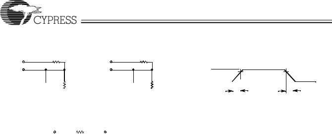
AC Test Loads and Waveforms |
|
|
|
|
|
5V |
R1 500Ω |
R1 500Ω |
|
ALL INPUT PULSES |
|
5V |
|
|
|
||
OUTPUT |
OUTPUT |
|
3.0V |
90% |
90% |
|
|
|
|
||
|
|
|
|
|
|
|
|
|
|
|
|
|
|
|
|
|
|
|
|
|
|
|
|
|
|
|
|
|
|
|
|
|
|
|
|
|
|
|
|
|
|
|
|
|
|
|
|
|
|
|
|
|
10% |
||
30 pF |
|
|
|
|
|
|
|
|
|
|
|
|
|
R2 |
|
5 pF |
|
|
|
|
|
|
|
|
|
|
|
|
|
R2 |
GND |
|
|
|
|
|
10% |
|
|
|
|||||||||
|
|
|
|
|
|
|
|
|
|
|
|
|
|
|
|
|
|
|
|
|
|
|
|
|
|
|
|
|
|
|
|
|
|
|
|
|
|
||||||||||||
INCLUDING |
|
|
|
|
|
|
|
|
|
|
|
|
|
|
333Ω |
INCLUDING |
|
|
|
|
|
|
|
|
|
|
|
|
|
|
333Ω |
|
≤ 5 ns |
|
|
|
|
|
|
|
|
≤ |
5 ns |
||||||
|
|
|
|
|
|
|
|
|
|
|
|
|
|
|
|
|
|
|
|
|
|
||||||||||||||||||||||||||||
|
|
|
|
|
|
|
|
|
|
|
|
|
|
|
|
|
|
|
|
|
|
|
|
|
|
|
|
|
|
|
|
|
|
|
|
|
|
|
|
|
|
||||||||
|
|
|
|
|
|
|
|
|
|
|
|
|
|
C460A–4 |
|
|
|
|
|
|
|
|
|
|
|
|
|
|
|
|
|
|
|
|
|
|
|
|
|
|
|
|
C460A–6 |
||||||
|
|
|
|
|
|
|
|
|
|
|
|
|
|
|
|
|
|
|
|
|
|
|
|
|
|
|
|
|
|
|
|
|
|
|
|
|
|
|
|
|
|
||||||||
JIG AND |
|
|
|
|
|
|
|
|
|
|
|
|
|
|
JIG AND |
|
|
|
|
|
|
|
|
|
|
|
|
|
C460A–5 |
|
|
|
|
|
|
|
|
|
|
|
|
|
|||||||
|
|
|
|
|
|
|
|
|
|
|
|
|
|
|
|
|
|
|
|
|
|
|
|
|
|
|
|
|
|
|
|
|
|
|
|
|
|
|
|||||||||||
|
|
|
|
|
|
|
|
|
|
|
|
|
|
|
|
|
|
|
|
|
|
|
|
|
|
|
|
|
|
|
|
|
|
|
|
|
|
|
|
|
|
||||||||
SCOPE |
|
|
|
(a) |
|
SCOPE |
|
|
|
|
|
(b) |
|
|
|
|
|
|
|
|
|
|
|
|
|
|
|
||||||||||||||||||||||
Equivalent to: |
|
|
THÉ VENIN EQUIVALENT |
|
|
|
|
|
|
|
|
|
|
|
|
|
|
|
|
|
|
|
|
|
|
|
|
|
|
|
|
|
|||||||||||||||||
OUTPUT |
|
|
|
|
|
|
|
200Ω |
|
2V |
|
|
|
|
|
|
|
|
|
|
|
|
|
|
|
|
|
|
|
|
|
|
|
|
|
|
|
|
|
||||||||||
|
|
|
|
|
|
|
|
|
|
|
|
|
|
|
|
|
|
|
|
|
|
|
|
|
|
|
|
|
|
|
|
|
|||||||||||||||||
|
|
|
|
|
|
|
|
|
|
|
|
|
|
|
|
|
|
|
|
|
|
|
|
|
|
|
|
|
|
|
|
||||||||||||||||||
Switching Characteristics Over the Operating Range[3, 6]
|
|
|
|
|
|
|
|
|
|
|
|
|
|
|
7C460A-10 |
7C460A-15 |
7C460A-25 |
|
|||
|
|
|
|
|
|
|
|
|
|
|
|
|
|
|
7C462A-10 |
7C462A-15 |
7C462A-25 |
|
|||
|
|
|
|
|
|
|
|
|
|
|
|
|
|
|
7C464A-10 |
7C464A-15 |
7C464A-25 |
|
|||
|
|
|
|
|
|
|
|
|
|
|
|
|
|
|
7C466A-10 |
7C466A-15 |
7C466A-25 |
|
|||
Parameter |
|
|
|
Description |
Min. |
Max. |
Min. |
Max. |
Min. |
Max. |
Unit |
||||||||||
|
|
|
|
|
|
|
|
|
|
||||||||||||
tRC |
|
Read Cycle Time |
20 |
|
25 |
|
35 |
|
ns |
||||||||||||
tA |
|
Access Time |
|
10 |
|
15 |
|
25 |
ns |
||||||||||||
tRR |
|
Read Recovery Time |
10 |
|
10 |
|
10 |
|
ns |
||||||||||||
tPR |
|
Read Pulse Width |
10 |
|
15 |
|
25 |
|
ns |
||||||||||||
tLZR |
|
Read LOW to Low Z |
3 |
|
3 |
|
3 |
|
ns |
||||||||||||
[7] |
|
Data Valid After Read HIGH |
3 |
|
3 |
|
3 |
|
ns |
||||||||||||
tDVR |
|
|
|
|
|||||||||||||||||
[7] |
|
Read HIGH to High Z |
|
15 |
|
15 |
|
18 |
ns |
||||||||||||
tHZR |
|
|
|
|
|||||||||||||||||
tWC |
|
Write Cycle Time |
20 |
|
25 |
|
35 |
|
ns |
||||||||||||
tPW |
|
Write Pulse Width |
10 |
|
15 |
|
25 |
|
ns |
||||||||||||
tHWZ |
|
Write HIGH to Low Z |
5 |
|
5 |
|
5 |
|
ns |
||||||||||||
tWR |
|
Write Recovery Time |
10 |
|
10 |
|
10 |
|
ns |
||||||||||||
tSD |
|
Data Set-Up Time |
9 |
|
9 |
|
9 |
|
ns |
||||||||||||
tHD |
|
Data Hold Time |
0 |
|
0 |
|
0 |
|
ns |
||||||||||||
tMRSC |
|
|
Cycle Time |
20 |
|
25 |
|
35 |
|
ns |
|||||||||||
|
MR |
|
|
|
|||||||||||||||||
tPMR |
|
|
Pulse Width |
10 |
|
15 |
|
25 |
|
ns |
|||||||||||
|
MR |
|
|
|
|||||||||||||||||
tRMR |
|
|
Recovery Time |
10 |
|
10 |
|
10 |
|
ns |
|||||||||||
|
MR |
|
|
|
|||||||||||||||||
tRPW |
|
Read HIGH to |
|
|
|
|
HIGH |
10 |
|
15 |
|
25 |
|
ns |
|||||||
|
MR |
|
|
|
|||||||||||||||||
tWPW |
|
Write HIGH to |
|
|
|
|
HIGH |
10 |
|
15 |
|
25 |
|
ns |
|||||||
|
MR |
|
|
|
|||||||||||||||||
tRTC |
|
Retransmit Cycle Time |
20 |
|
25 |
|
35 |
|
ns |
||||||||||||
tPRT |
|
Retransmit Pulse Width |
10 |
|
15 |
|
25 |
|
ns |
||||||||||||
tRTR |
|
Retransmit Recovery Time |
10 |
|
10 |
|
10 |
|
ns |
||||||||||||
tEFL |
|
|
to |
|
|
|
LOW |
|
20 |
|
25 |
|
35 |
ns |
|||||||
|
MR |
EF |
|
|
|
|
|||||||||||||||
tHFH |
|
|
to |
|
|
|
HIGH |
|
20 |
|
25 |
|
35 |
ns |
|||||||
|
MR |
HF |
|
|
|
||||||||||||||||
tFFH |
|
|
to |
|
HIGH |
|
20 |
|
25 |
|
35 |
ns |
|||||||||
|
MR |
FF |
|
|
|
||||||||||||||||
tREF |
|
Read LOW to |
|
|
|
|
LOW |
|
10 |
|
15 |
|
25 |
ns |
|||||||
|
EF |
|
|
|
|
||||||||||||||||
tRFF |
|
Read HIGH to |
|
|
HIGH |
|
10 |
|
15 |
|
25 |
ns |
|||||||||
|
FF |
|
|
|
|||||||||||||||||
Notes: |
|
|
|
|
|
|
|
|
|
|
|
|
|
|
|
|
|
|
|
|
|
6.Test conditions assume signal transmission time of 5 ns or less, timing reference levels of 1.5V and output loading of the specified IOL/IOH and 30-pF load capacitance, as in part (a) of AC Test Loads, unless otherwise specified.
7.tHZR and tDVR use capacitance loading as in part (b) of AC Test Loads.
Document #: 38-06011 Rev. *A |
Page 3 of 15 |

|
|
|
|
|
|
|
|
|
|
|
|
|
|
CY7C460A/CY7C462A |
|||
|
|
|
|
|
|
|
|
|
|
|
|
|
|
CY7C464A/CY7C466A |
|||
|
|
|
|
|
|
|
|
|
|
|
|
|
|
|
|
|
|
Switching Characteristics Over the Operating Range[3, 6] (continued) |
|
|
|
|
|||||||||||||
|
|
|
|
|
|
|
|
|
|
|
7C460A-10 |
7C460A-15 |
7C460A-25 |
|
|||
|
|
|
|
|
|
|
|
|
|
|
7C462A-10 |
7C462A-15 |
7C462A-25 |
|
|||
|
|
|
|
|
|
|
|
|
|
|
7C464A-10 |
7C464A-15 |
7C464A-25 |
|
|||
|
|
|
|
|
|
|
|
|
|
|
7C466A-10 |
7C466A-15 |
7C466A-25 |
|
|||
|
|
|
|
|
|
|
|
|
|||||||||
Parameter |
Description |
Min. |
Max. |
Min. |
Max. |
Min. |
Max. |
Unit |
|||||||||
|
|
|
|
|
|
|
|
|
|
|
|
|
|
|
|||
tWEF |
Write HIGH to |
|
|
|
|
|
HIGH |
|
10 |
|
15 |
|
25 |
ns |
|||
EF |
|
|
|
|
|||||||||||||
tWFF |
Write LOW to |
|
|
|
|
LOW |
|
10 |
|
15 |
|
25 |
ns |
||||
FF |
|
|
|
|
|||||||||||||
tWHF |
Write LOW to |
|
|
|
|
|
LOW |
|
10 |
|
15 |
|
35 |
ns |
|||
HF |
|
|
|
||||||||||||||
tRHF |
Read HIGH to |
|
|
|
|
HIGH |
|
10 |
|
15 |
|
35 |
ns |
||||
HF |
|
|
|
||||||||||||||
tRAE |
Effective Read from Write |
|
10 |
|
15 |
|
25 |
ns |
|||||||||
|
HIGH |
|
|
|
|
|
|
|
|||||||||
tRPE |
Effective Read Pulse Width |
10 |
|
15 |
|
25 |
|
ns |
|||||||||
|
After EF HIGH |
|
|
|
|
|
|
|
|||||||||
tWAF |
Effective Write from Read |
|
10 |
|
15 |
|
25 |
ns |
|||||||||
|
HIGH |
|
|
|
|
|
|
|
|||||||||
tWPF |
Effective Write Pulse |
10 |
|
15 |
|
25 |
|
ns |
|||||||||
|
Width After FF HIGH |
|
|
|
|
|
|
|
|||||||||
tXOL |
Expansion Out LOW |
|
10 |
|
15 |
|
25 |
ns |
|||||||||
|
Delay from Clock |
|
|
|
|
|
|
|
|||||||||
tXOH |
Expansion Out HIGH |
|
10 |
|
15 |
|
25 |
ns |
|||||||||
|
Delay from Clock |
|
|
|
|
|
|
|
|||||||||
Document #: 38-06011 Rev. *A |
Page 4 of 15 |

CY7C460A/CY7C462A
CY7C464A/CY7C466A
Switching Waveforms[7]
Asynchronous Read and Write
|
|
|
|
|
|
|
|
|
|
|
|
tRC |
|
|
|
|
|
|
|
|
tPR |
|
|
|
|
|
|
|
|
|
|||||||||||||
|
|
|
|
|
|
|
|
tA |
|
|
|
|
|
|
|
|
|
tRR |
|
|
|
|
tA |
|
|
|
|
|
|
|
|
|
|
|
|
|
|||||||
|
|
|
|
|
|
|
|
|
|
|
|
|
|
|
|
|
|
|
|
|
|
|
|
|
|
|
|
|
|
|
|
|
|
||||||||||
|
R |
|
|
|
|
|
|
|
|
|
|
|
|
|
|
|
|
|
|
|
|
|
|
|
|
|
|
|
|
|
|
|
|
|
|
|
|
|
|
|
|
|
|
|
|
|
|
|
|
|
|
|
|
|
|
|
|
|
|
|
|
|
|
|
|
|
|
|
|
|
|
|
|
|
|
|
|
|
|
|
|
|
|
|
|||
|
|
|
|
|
|
|
|
|
|
|
|
|
|
|
|
|
|
|
|
|
|
|
|
|
|
|
|
|
|
|
|
|
|
||||||||||
|
|
|
|
|
|
|
|
|
|
|
|
|
|
|
|
|
|
|
|
|
|
|
|
|
|
|
|
|
|
|
|
|
|
|
|
|
|
|
|
|
|
|
|
|
|
|
|
|
|
|
|
|
|
|
|
|
|
|
|
|
|
|
|
|
|
|
|
|
|
|
|
|
|
|
|
|
|
|
|
|
|
|
|||||
Q0− Q 8 |
|
|
|
|
tLZR |
|
|
|
|
|
|
|
|
|
|
|
tDVR |
|
|
|
|
|
|
|
|
|
|
|
|
|
tHZR |
|
|
|
|
|
|||||||
|
|
|
|
|
|
|
|
|
|
|
|
|
|
|
|
|
|
|
|
|
|
|
|
|
|
|
|
|
|
|
|
|
|||||||||||
|
|
|
|
|
|
|
|
|
|
|
|
|
|
|
|
|
|
|
|
|
|
|
|
|
|
|
|
|
|
|
|
|
|
|
|
|
|
|
|
|
|||
|
|
|
|
|
|
|
|
|
|
|
|
|
|
DATA VALID |
|
|
|
|
|
|
|
|
DATA VALID |
|
|
|
|
||||||||||||||||
|
|
|
|
|
|
|
|
|
|
|
|
||||||||||||||||||||||||||||||||
|
|
|
|
|
|
|
|
|
|
|
|
|
|
|
|
|
|
|
|
|
|
|
|
|
|
|
|
|
|
|
|
|
|
|
|
|
|
|
|
|
|
|
|
tWC
tPW  tWR
tWR  tPW
tPW
|
W |
|
|
|
|
|
|
|
tSD |
tHD |
|
tSD |
tHD |
|
D0− D 8 |
DATA VALID |
|
DATA VALID |
||
|
|
|
|
|
|
C460A–7 |
Master |
Reset |
|
tMRSC [10] |
|
|
|
|
MR |
|
tPMR |
|
|
|
|
|
|
|
|
|
|
|
R, W [9] |
|
tRPW |
|
|
|
|
|
tEFL |
|
|
|
|
|
EF |
tWPW |
tRMR |
|
|
|
|
|
|
|
|||
|
|
tHFH |
|
|
|
|
|
HF |
|
|
|
|
|
|
|
tFFH |
|
|
|
|
|
FF |
|
|
|
|
C460A–8 |
Half Full Flag |
|
|
|
|
|
|
|
HALF FULL |
|
HALF FULL+1 |
|
HALF FULL |
|
|
W |
|
|
|
|
|
|
|
|
|
|
|
tRHF |
|
R |
|
|
|
|
|
|
|
tWHF |
|
|
|
|
|
HF |
|
|
|
|
|
|
|
|
|
|
|
C460A–9 |
Notes:
8.A HIGH-to-LOW transition of either the write or read strobe causes a HIGH-to-LOW transition of the responding flag. Correspondingly, a LOW-to-HIGH strobe transition causes a LOW-to-HIGH flag transition.
9.W and R = VIH around the rising edge of MR.
10. tMSRC = t PMR + t RMR
Document #: 38-06011 Rev. *A |
Page 5 of 15 |
CY7C460A/CY7C462A
CY7C464A/CY7C466A
Switching Waveforms[7] (continued)
Last Write to First Read Full Flag
LAST WRITE
R
W
 tWFF
tWFF
FF
|
ADDITIONAL |
|
FIRST READ |
READS |
FIRST WRITE |
tRFF |
C460A–10
Last READ to First WRITE Empty Flag
|
|
|
ADDITIONAL |
|
W |
LAST READ |
FIRST WRITE |
WRITES |
FIRST READ |
|
|
|
|
|
R |
|
|
|
|
|
tREF |
tWEF |
|
|
EF |
|
|
|
|
|
tA |
|
|
|
DATA OUT |
VALID |
|
|
VALID |
|
|
|
|
C460A–11 |
Retransmit[11,12] |
|
|
|
|
|
tRTC |
FL/RT |
tPRT |
|
|
R,W |
tRTR |
|
|
tRTC |
tRTR |
C460A–12
Notes:
11.tRTC = tPRT + tRTR.
12.EF, HF, and FF may change state during retransmit as a result of the offset of the read and write pointers, but flags will be valid at tRTC, except for the CY7C46x-20 (Military), whose flags will be valid after tRTC + 10 ns.
Document #: 38-06011 Rev. *A |
Page 6 of 15 |
|
|
CY7C460A/CY7C462A |
|
|
CY7C464A/CY7C466A |
Switching Waveforms[7] (continued) |
|
|
Full Flag and Write Data Flow-Through Mode |
|
|
R |
|
|
|
tWAF |
tWPF |
W |
|
|
|
tRFF |
tWFF |
|
|
|
FF |
|
tHD |
|
|
|
DATA IN |
|
DATA VALID |
|
tA |
tSD |
DATA OUT |
DATA VALID |
|
|
|
C460A–13 |
Empty Flag and Read Data Flow-Through Mode |
|
|
DATA IN |
|
|
W |
|
|
|
tRAE |
|
R |
|
|
|
|
tRPE |
|
|
tREF |
EF |
tWEF |
tA |
|
||
|
tHWZ |
|
DATA OUT |
|
DATA VALID |
|
|
C460A–14 |
Document #: 38-06011 Rev. *A |
Page 7 of 15 |
|
CY7C460A/CY7C462A |
|
CY7C464A/CY7C466A |
Switching Waveforms[7] (continued) |
|
Expansion TimingDiagrams |
|
W |
|
tWR |
|
t XOL |
t XOH |
[13] |
|
XO1(XI2) |
|
tHD |
t |
tSD |
HD |
tSD |
D0− D 8 |
|
|
DATA VALID |
|
|
|
|
DATA VALID |
|
|
|
|
|
C460A–15
|
|
R |
|
|
|
|
|
|
|
tRR |
|
|
|
|
tXOL |
tXOH |
|
|
|
) [13] |
|
|
|
XO (XI |
2 |
|
|
|
|
1 |
|
|
|
|
|
|
|
|
|
|
tHZR |
|
|
tLZR |
tDVR |
|
tDVR |
|
|
|
|
||
Q0 − Q8 |
DATA |
|
DATA |
||
|
|
|
VALID |
|
VALID |
|
|
|
tA |
tA |
C460A–16 |
Note:
13. Expansion out of device 1 (XO1) is connected to expansion in of device 2 (XI2).
Architecture
Resetting the FIFO
Upon power-up, the FIFO must be reset with a master reset (MR) cycle. This causes the FIFO to enter the empty condition signified by the Empty flag (EF) being LOW, and both the Half Full (HF), and Full flags (FF) being HIGH. Read (R) and Write
(W) must be HIGH tRPW/tWPW before and tRMR after the rising edge of MR for a valid reset cycle. If reading from the FIFO
after a reset cycle is attempted, the outputs will all be in the high-impedance state.
Writing Data to the FIFO
The availability of at least one empty location is indicated by a HIGH FF. The falling edge of W initiates a write cycle. Data appearing at the inputs (D0− D8) tSD before and tHD after the rising edge of W will be stored sequentially in the FIFO.
The EF LOW-to-HIGH transition occurs tWEF after the first LOW-to-HIGH transition of W for an empty FIFO. HF goes
LOW tWHF after the falling edge of W following the FIFO actually being half full. Therefore, the HF is active once the FIFO is filled to half its capacity plus one word. HF will remain LOW while less than one half of total memory is available for writing.
The LOW-to-HIGH transition of HF occurs tRHF after the rising edge of R when the FIFO goes from half full +1 to half full. HF
is available in standalone and width expansion modes. FF goes LOW tWFF after the falling edge of W, during the cycle in which the last available location is filled. Internal logic prevents overrunning a full FIFO. Writes to a full FIFO are ignored and the write pointer is not incremented. FF goes HIGH tRFF after a read from a full FIFO.
Reading Data from the FIFO
The falling edge of R initiates a read cycle if the EF is not LOW. Data outputs (Q0− Q8) are in a high-impedance condition between read operations (R HIGH), when the FIFO is empty, or when the FIFO is not the active device in the depth expansion mode.
When one word is in the FIFO, the falling edge of R initiates a HIGH-to-LOW transition of EF. When the FIFO is empty, the outputs are in a high-impedance state. Reads to an empty FIFO are ignored and do not increment the read pointer. From the empty condition, the FIFO can be read tWEF after a valid write.
Retransmit
The retransmit feature is beneficial when transferring packets of data. It enables the receipt of data to be acknowledged by the receiver and retransmitted if necessary. The retransmit (RT) input is active in the standalone and width expansion modes. The retransmit feature is intended for use when a
Document #: 38-06011 Rev. *A |
Page 8 of 15 |

CY7C460A/CY7C462A
CY7C464A/CY7C466A
number of writes equal-to-or-less-than the depth of the FIFO have occurred since the last MR cycle. A LOW pulse on RT resets the internal read pointer to the first physical location of
the FIFO. R and W must both be HIGH while and tRTR after retransmit is LOW. With every read cycle after retransmit, pre-
viously accessed data is read and the read pointer incremented until equal to the write pointer. Full, Half Full, and Empty flags are governed by the relative locations of the read and write pointers and are updated during a retransmit cycle. Data written to the FIFO after activation of RT are transmitted also.
The full depth of the FIFO can be repeatedly retransmitted.
Standalone/Width Expansion Modes
Standalone and width expansion modes are set by grounding expansion in (XI) and tying first load (FL) to VCC prior to a MR cycle. FIFOs can be expanded in width to provide word widths greater than nine in increments of nine. During width expansion mode, all control line inputs are common to all devices, and flag outputs from any device can be monitored.
Depth Expansion Mode (see Figure 1)
Depth expansion mode is entered when, during a MR cycle, expansion out (XO) of one device is connected to expansion in (XI) of the next device, with XO of the last device connected to XI of the first device. In the depth expansion mode, the first load (FL) input, when grounded, indicates that this is the first part to be loaded. All other devices must have this pin HIGH. To enable the correct FIFO, XO is pulsed LOW when the last physical location of the previous FIFO is written to and is pulsed LOW again when the last physical location is read. Only one FIFO is enabled for Read and one is enabled for Write at any given time. All other devices are in standby.
FIFOs can also be expanded simultaneously in depth and width. Consequently, any depth or width FIFO can be created with word widths in increments of nine. When expanding in depth, a composite FF is created by ORing the FFs together. Likewise, a composite EF is created by ORing EFs together. HF and RT functions are not available in depth expansion mode.
|
|
|
XO |
|
|
R |
|
W |
|
|
|
|
|
|
|
FF |
|
EF |
|
|
D0-8 |
9 |
9 |
CY7C460A |
|
9 |
Q0-8 |
|
|
|
CY7C462A |
|
|
|
|
|
|
CY7C464A |
|
|
|
|
|
|
CY7C466A |
|
|
|
|
|
|
|
FL |
|
VCC |
|
|
|
|
|
|
|
|
|
|
XI |
|
|
|
|
|
|
XO |
|
|
|
FULL |
|
FF |
|
EF |
|
EMPTY |
|
|
9 |
CY7C460A |
|
|
|
|
|
|
CY7C462A |
|
|
|
|
|
|
CY7C464A |
|
|
|
|
|
|
CY7C466A |
|
|
|
|
|
|
|
FL |
|
|
|
|
|
XI |
|
|
|
|
|
|
XO |
|
|
|
|
|
FF |
* |
EF |
|
|
|
|
|
|
|
||
|
|
9 |
CY7C460A |
|
|
|
|
|
CY7C462A |
|
|
|
|
|
|
|
|
|
|
|
|
|
|
CY7C464A |
|
|
|
|
|
|
CY7C466A |
|
|
|
|
RS |
|
|
FL |
|
|
|
|
|
XI |
|
|
|
|
|
|
|
* FIRSTDEVICE |
|
|
|
|
|
|
|
|
C460A–17 |
Figure 1. Depth Expansion
Document #: 38-06011 Rev. *A |
Page 9 of 15 |

CY7C460A/CY7C462A
CY7C464A/CY7C466A
Ordering Information
8K x 9 Asynchronous FIFO
Speed |
|
Package |
|
Operating |
(ns) |
Ordering Code |
Name |
Package Type |
Range |
|
|
|
|
|
10 |
CY7C460A-10JC |
J65 |
32-Lead Plastic Leaded Chip Carrier |
Commercial |
|
|
|
|
|
|
CY7C460A-10PC |
P15 |
28-Lead (600-Mil) Molded DIP |
|
|
|
|
|
|
|
CY7C460A-10PTC |
P21 |
28-Lead (300-Mil) Molded DIP |
|
|
|
|
|
|
|
CY7C460A-10JI |
J65 |
32-Lead Plastic Leaded Chip Carrier |
Industrial |
|
|
|
|
|
15 |
CY7C460A-15JC |
J65 |
32-Lead Plastic Leaded Chip Carrier |
Commercial |
|
|
|
|
|
|
CY7C460A-15PC |
P15 |
28-Lead (600-Mil) Molded DIP |
|
|
|
|
|
|
|
CY7C460A-15PTC |
P21 |
28-Lead (300-Mil) Molded DIP |
|
|
|
|
|
|
25 |
CY7C460A-25JC |
J65 |
32-Lead Plastic Leaded Chip Carrier |
Commercial |
|
|
|
|
|
|
CY7C460A-25PC |
P15 |
28-Lead (600-Mil) Molded DIP |
|
|
|
|
|
|
|
CY7C460A-25PTC |
P21 |
28-Lead (300-Mil) Molded DIP |
|
|
|
|
|
|
16K x 9 Asynchronous FIFO |
|
|
|
|
|
|
|
|
|
Speed |
|
Package |
|
Operating |
(ns) |
Ordering Code |
Name |
Package Type |
Range |
|
|
|
|
|
10 |
CY7C462A-10JC |
J65 |
32-Lead Plastic Leaded Chip Carrier |
Commercial |
|
|
|
|
|
|
CY7C462A-10PC |
P15 |
28-Lead (600-Mil) Molded DIP |
|
|
|
|
|
|
|
CY7C462A-10PTC |
P21 |
28-Lead (300-Mil) Molded DIP |
|
|
|
|
|
|
|
CY7C462A-10JI |
J65 |
32-Lead Plastic Leaded Chip Carrier |
Industrial |
|
|
|
|
|
15 |
CY7C462A-15JC |
J65 |
32-Lead Plastic Leaded Chip Carrier |
Commercial |
|
|
|
|
|
|
CY7C462A-15PC |
P15 |
28-Lead (600-Mil) Molded DIP |
|
|
|
|
|
|
|
CY7C462A-15PTC |
P21 |
28-Lead (300-Mil) Molded DIP |
|
|
|
|
|
|
25 |
CY7C462A-25JC |
J65 |
32-Lead Plastic Leaded Chip Carrier |
Commercial |
|
|
|
|
|
|
CY7C462A-25PC |
P15 |
28-Lead (600-Mil) Molded DIP |
|
|
|
|
|
|
|
CY7C462A-25PTC |
P21 |
28-Lead (300-Mil) Molded DIP |
|
|
|
|
|
|
32K x 9 Asynchronous FIFO |
|
|
|
|
|
|
|
|
|
Speed |
|
Package |
|
Operating |
(ns) |
Ordering Code |
Name |
Package Type |
Range |
|
|
|
|
|
10 |
CY7C464A-10JC |
J65 |
32-Lead Plastic Leaded Chip Carrier |
Commercial |
|
|
|
|
|
|
CY7C464A-10PC |
P15 |
28-Lead (600-Mil) Molded DIP |
|
|
|
|
|
|
|
CY7C464A-10PTC |
P21 |
28-Lead (300-Mil) Molded DIP |
|
|
|
|
|
|
|
CY7C464A-10JI |
J65 |
32-Lead Plastic Leaded Chip Carrier |
Industrial |
|
|
|
|
|
15 |
CY7C464A-15JC |
J65 |
32-Lead Plastic Leaded Chip Carrier |
Commercial |
|
|
|
|
|
|
CY7C464A-15PC |
P15 |
28-Lead (600-Mil) Molded DIP |
|
|
|
|
|
|
|
CY7C464A-15PTC |
P21 |
28-Lead (300-Mil) Molded DIP |
|
|
|
|
|
|
|
CY7C464A-15LMB |
L55 |
32-Pin Rectangular Leadless Chip Carrier |
Military |
|
|
|
|
|
25 |
CY7C464A-25JC |
J65 |
32-Lead Plastic Leaded Chip Carrier |
Commercial |
|
|
|
|
|
|
CY7C464A-25PC |
P15 |
28-Lead (600-Mil) Molded DIP |
|
|
|
|
|
|
|
CY7C464A-25PTC |
P21 |
28-Lead (300-Mil) Molded DIP |
|
|
|
|
|
|
Document #: 38-06011 Rev. *A |
|
|
Page 10 of 15 |
|