

Курсовая работа1 / ampl
.pdfa |
Low Distortion |
|
1.0 GHz Differential Amplifier |
||
|
|
|
|
|
AD8350 |
|
|
|
FEATURES
High Dynamic Range
Output IP3: +28 dBm: Re 50 @ 250 MHz
Low Noise Figure: 5.9 dB @ 250 MHz Two Gain Versions:
AD8350-15: 15 dB AD8350-20: 20 dB
–3 dB Bandwidth: 1.0 GHz
Single Supply Operation: 5 V to 10 V Supply Current: 28 mA Input/Output Impedance: 200
Single-Ended or Differential Input Drive
8-Lead SOIC Package and 8-Lead microSOIC Package
APPLICATIONS
Cellular Base Stations
Communications Receivers
RF/IF Gain Block
Differential A-to-D Driver
SAW Filter Interface
Single-Ended-to-Differential Conversion
High Performance Video
High Speed Data Transmission
PRODUCT DESCRIPTION
The AD8350 series are high performance fully-differential amplifiers useful in RF and IF circuits up to 1000 MHz. The amplifier has excellent noise figure of 5.9 dB at 250 MHz. It offers a high output third order intercept (OIP3) of +28 dBm at 250 MHz. Gain versions of 15 dB and 20 dB are offered.
The AD8350 is designed to meet the demanding performance requirements of communications transceiver applications. It enables a high dynamic range differential signal chain, with exceptional linearity and increased common-mode rejection. The device can be used as a general purpose gain block, an A-to-D driver, and high speed data interface driver, among other functions. The AD8350 input can also be used as a single- ended-to-differential converter.
FUNCTIONAL BLOCK DIAGRAM
8-Lead SOIC and SOIC Packages (with Enable)
IN+ |
1 |
|
|
8 |
IN– |
ENBL |
2 |
+ |
– |
7 |
GND |
VCC |
3 |
|
|
6 |
GND |
OUT+ |
4 |
|
|
5 |
OUT– |
|
|
AD8350 |
|
|
|
The amplifier can be operated down to 5 V with an OIP3 of +28 dBm at 250 MHz and slightly reduced distortion performance. The wide bandwidth, high dynamic range and temperature stability make this product ideal for the various RF and IF frequencies required in cellular, CATV, broadband, instrumentation and other applications.
The AD8350 is offered in an 8-lead single SOIC package andSOIC package. It operates from 5 V and 10 V power supplies, drawing 28 mA typical. The AD8350 offers a power enable function for power-sensitive applications. The AD8350 is fabricated using Analog Devices’ proprietary high speed complementary bipolar process. The device is available in the industrial (–40°C to +85°C) temperature range.
REV. A
Information furnished by Analog Devices is believed to be accurate and reliable. However, no responsibility is assumed by Analog Devices for its use, nor for any infringements of patents or other rights of third parties that may result from its use. No license is granted by implication or otherwise under any patent or patent rights of Analog Devices.
One Technology Way, P.O. Box 9106, Norwood, MA 02062-9106, U.S.A.
Tel: 781/329-4700 |
www.analog.com |
Fax: 781/326-8703 |
© Analog Devices, Inc., 2001 |
|
(@ 25 C, VS = 5 V, G = 15 dB, unless otherwise noted. All specifications refer to |
|
||||
AD8350–SPECIFICATIONS differential inputs and differential outputs unless noted.) |
|
|
|
|
||
Parameter |
Conditions |
Min |
Typ |
Max |
|
Unit |
|
|
|
|
|
|
|
DYNAMIC PERFORMANCE |
|
|
|
|
|
|
–3 dB Bandwidth |
VS = 5 V, VOUT = 1 V p-p |
|
0.9 |
|
|
GHz |
|
VS = 10 V, VOUT = 1 V p-p |
|
1.1 |
|
|
GHz |
Bandwidth for 0.1 dB Flatness |
VS = 5 V, VOUT = 1 V p-p |
|
90 |
|
|
MHz |
|
VS = 10 V, VOUT = 1 V p-p |
|
90 |
|
|
MHz |
Slew Rate |
VOUT = 1 V p-p |
|
2000 |
|
|
V/µs |
Settling Time |
0.1%, VOUT = 1 V p-p |
|
10 |
|
|
ns |
Gain (S21)1 |
VS = 5 V, f = 50 MHz |
14 |
15 |
16 |
|
dB |
Gain Supply Sensitivity |
VS = 5 V to 10 V, f = 50 MHz |
|
0.003 |
|
|
dB/V |
Gain Temperature Sensitivity |
TMIN to TMAX |
|
–0.002 |
|
|
dB/°C |
Isolation (S12)1 |
f = 50 MHz |
|
–18 |
|
|
dB |
NOISE/HARMONIC PERFORMANCE |
|
|
|
|
|
|
50 MHz Signal |
|
|
|
|
|
|
Second Harmonic |
VS = 5 V, VOUT = 1 V p-p |
|
–66 |
|
|
dBc |
|
VS = 10 V, VOUT = 1 V p-p |
|
–67 |
|
|
dBc |
Third Harmonic |
VS = 5 V, VOUT = 1 V p-p |
|
–65 |
|
|
dBc |
Output Second Order Intercept2 |
VS = 10 V, VOUT = 1 V p-p |
|
–70 |
|
|
dBc |
VS = 5 V |
|
58 |
|
|
dBm |
|
Output Third Order Intercept2 |
VS = 10 V |
|
58 |
|
|
dBm |
VS = 5 V |
|
28 |
|
|
dBm |
|
250 MHz Signal |
VS = 10 V |
|
29 |
|
|
dBm |
|
|
|
|
|
|
|
Second Harmonic |
VS = 5 V, VOUT = 1 V p-p |
|
–48 |
|
|
dBc |
|
VS = 10 V, VOUT = 1 V p-p |
|
–49 |
|
|
dBc |
Third Harmonic |
VS = 5 V, VOUT = 1 V p-p |
|
–52 |
|
|
dBc |
Output Second Order Intercept2 |
VS = 10 V, VOUT = 1 V p-p |
|
–61 |
|
|
dBc |
VS = 5 V |
|
39 |
|
|
dBm |
|
Output Third Order Intercept2 |
VS = 10 V |
|
40 |
|
|
dBm |
VS = 5 V |
|
24 |
|
|
dBm |
|
1 dB Compression Point (RTI)2 |
VS = 10 V |
|
28 |
|
|
dBm |
VS = 5 V |
|
2 |
|
|
dBm |
|
|
VS = 10 V |
|
5 |
|
|
dBm |
Voltage Noise (RTI) |
f = 150 MHz |
|
1.7 |
|
|
nV/√Hz |
Noise Figure |
f = 150 MHz |
|
6.8 |
|
|
dB |
|
|
|
|
|
|
|
INPUT/OUTPUT CHARACTERISTICS |
|
|
± 1 |
|
|
|
Differential Offset Voltage (RTI) |
VOUT+ – VOUT– |
|
|
|
mV |
|
Differential Offset Drift |
TMIN to TMAX |
|
0.02 |
|
|
mV/°C |
Input Bias Current |
|
|
15 |
|
|
µA |
Input Resistance |
Real |
|
200 |
|
|
Ω |
CMRR |
f = 50 MHz |
|
–67 |
|
|
dB |
Output Resistance |
Real |
|
200 |
|
|
Ω |
|
|
|
|
|
|
|
POWER SUPPLY |
|
|
|
|
|
|
Operating Range |
|
4 |
|
11.0 |
|
V |
Quiescent Current |
Powered Up, VS = 5 V |
25 |
28 |
32 |
|
mA |
|
Powered Down, VS = 5 V |
3 |
3.8 |
5.5 |
|
mA |
|
Powered Up, VS = 10 V |
27 |
30 |
34 |
|
mA |
|
Powered Down, VS = 10 V |
3 |
4 |
6.5 |
|
mA |
Power-Up/Down Switching |
f = 50 MHz, VS ∆ = 1 V p-p |
|
15 |
|
|
ns |
Power Supply Rejection Ratio |
|
–58 |
|
|
dB |
|
|
|
|
|
|
|
|
OPERATING TEMPERATURE RANGE |
|
–40 |
|
+85 |
|
°C |
|
|
|
|
|
|
|
NOTES
1See Tables II–III for complete list of S-Parameters. 2Re: 50 Ω.
Specifications subject to change without notice.
–2– |
REV. A |
AD8350
AD8350-20–SPECIFICATIONS (@ 25 C, VS = 5 V, G = 20 dB, unless otherwise noted. All specifications refer to differential inputs and differential outputs unless noted.)
Parameter |
Conditions |
Min |
Typ |
Max |
Unit |
|
|
|
|
|
|
DYNAMIC PERFORMANCE |
|
|
|
|
|
–3 dB Bandwidth |
VS = 5 V, VOUT = 1 V p-p |
|
0.7 |
|
GHz |
|
VS = 10 V, VOUT = 1 V p-p |
|
0.9 |
|
GHz |
Bandwidth for 0.1 dB Flatness |
VS = 5 V, VOUT = 1 V p-p |
|
90 |
|
MHz |
|
VS = 10 V, VOUT = 1 V p-p |
|
90 |
|
MHz |
Slew Rate |
VOUT = 1 V p-p |
|
2000 |
|
V/µs |
Settling Time |
0.1%, VOUT = 1 V p-p |
|
15 |
|
ns |
Gain (S21)1 |
VS = 5 V, f = 50 MHz |
19 |
20 |
21 |
dB |
Gain Supply Sensitivity |
VS = 5 V to 10 V, f = 50 MHz |
|
0.003 |
|
dB/V |
Gain Temperature Sensitivity |
TMIN to TMAX |
|
–0.002 |
|
dB/°C |
Isolation (S12)1 |
f = 50 MHz |
|
–22 |
|
dB |
NOISE/HARMONIC PERFORMANCE |
|
|
|
|
|
50 MHz Signal |
|
|
|
|
|
Second Harmonic |
VS = 5 V, VOUT = 1 V p-p |
|
–65 |
|
dBc |
|
VS = 10 V, VOUT = 1 V p-p |
|
–66 |
|
dBc |
Third Harmonic |
VS = 5 V, VOUT = 1 V p-p |
|
–66 |
|
dBc |
Output Second Order Intercept2 |
VS = 10 V, VOUT = 1 V p-p |
|
–70 |
|
dBc |
VS = 5 V |
|
56 |
|
dBm |
|
Output Third Order Intercept2 |
VS = 10 V |
|
56 |
|
dBm |
VS = 5 V |
|
28 |
|
dBm |
|
250 MHz Signal |
VS = 10 V |
|
29 |
|
dBm |
|
|
|
|
|
|
Second Harmonic |
VS = 5 V, VOUT = 1 V p-p |
|
–45 |
|
dBc |
|
VS = 10 V, VOUT = 1 V p-p |
|
–46 |
|
dBc |
Third Harmonic |
VS = 5 V, VOUT = 1 V p-p |
|
–55 |
|
dBc |
Output Second Order Intercept2 |
VS = 10 V, VOUT = 1 V p-p |
|
–60 |
|
dBc |
VS = 5 V |
|
37 |
|
dBm |
|
Output Third Order Intercept2 |
VS = 10 V |
|
38 |
|
dBm |
VS = 5 V |
|
24 |
|
dBm |
|
1 dB Compression Point (RTI)2 |
VS = 10 V |
|
28 |
|
dBm |
VS = 5 V |
|
–2.6 |
|
dBm |
|
|
VS = 10 V |
|
1.8 |
|
dBm |
Voltage Noise (RTI) |
f = 150 MHz |
|
1.7 |
|
nV/√Hz |
Noise Figure |
f = 150 MHz |
|
5.6 |
|
dB |
|
|
|
|
|
|
INPUT/OUTPUT CHARACTERISTICS |
|
|
± 1 |
|
|
Differential Offset Voltage (RTI) |
VOUT+ – VOUT– |
|
|
mV |
|
Differential Offset Drift |
TMIN to TMAX |
|
0.02 |
|
mV/°C |
Input Bias Current |
|
|
15 |
|
µA |
Input Resistance |
Real |
|
200 |
|
Ω |
CMRR |
f = 50 MHz |
|
–52 |
|
dB |
Output Resistance |
Real |
|
200 |
|
Ω |
|
|
|
|
|
|
POWER SUPPLY |
|
|
|
|
|
Operating Range |
|
4 |
|
11.0 |
V |
Quiescent Current |
Powered Up, VS = 5 V |
25 |
28 |
32 |
mA |
|
Powered Down, VS = 5 V |
3 |
3.8 |
5.5 |
mA |
|
Powered Up, VS = 10 V |
27 |
30 |
34 |
mA |
|
Powered Down, VS = 10 V |
3 |
4 |
6.5 |
mA |
Power-Up/Down Switching |
f = 50 MHz, VS ∆ = 1 V p-p |
|
15 |
|
ns |
Power Supply Rejection Ratio |
|
–45 |
|
dB |
|
OPERATING TEMPERATURE RANGE |
|
–40 |
|
+85 |
°C |
|
|
|
|
|
|
NOTES
1See Tables II–III for complete list of S-Parameters. 2Re: 50 Ω.
REV. A |
–3– |

AD8350
ABSOLUTE MAXIMUM RATINGS* |
|
Supply Voltage, VS . . . . . . . . . . . . . . . . . . . . |
. . . . . . . . . 11 V |
Input Power Differential . . . . . . . . . . . . . . . . |
. . . . . . +8 dBm |
Internal Power Dissipation . . . . . . . . . . . . . . |
. . . . . . 400 mW |
θJA SOIC (R) . . . . . . . . . . . . . . . . . . . . . . . . . |
. . . . . . 100°C/W |
θJA µSOIC (RM) . . . . . . . . . . . . . . . . . . . . . . |
. . . . . . 133°C/W |
Maximum Junction Temperature . . . . . . . . . |
. . . . . . . . 125°C |
Operating Temperature Range . . . . . . . . . . . |
–40°C to +85°C |
Storage Temperature Range . . . . . . . . . . . . |
–65°C to +150°C |
Lead Temperature Range (Soldering 60 sec) . |
. . . . . . . . 300°C |
*Stresses above those listed under Absolute Maximum Ratings may cause permanent damage to the device. This is a stress rating only; functional operation of the device at these or any other conditions above those indicated in the operational section of this specification is not implied. Exposure to absolute maximum rating conditions for extended periods may affect device reliability.
PIN CONFIGURATION
IN+ |
|
|
|
IN– |
1 |
|
8 |
||
ENBL |
2 |
AD8350 |
|
GND |
7 |
||||
VCC |
3 |
TOP VIEW |
|
GND |
(Not to Scale) |
6 |
|||
OUT+ |
4 |
|
|
OUT– |
|
5 |
|||
|
|
|
|
|
PIN FUNCTION DESCRIPTIONS
Pin |
Function |
Description |
|
|
|
1, 8 |
IN+, IN– |
Differential Inputs. IN+ and IN– |
|
|
should be ac-coupled (pins have a dc |
|
|
bias of midsupply). Differential input |
|
|
impedance is 200 Ω. |
2 |
ENBL |
Power-up Pin. A high level (5 V) enables |
|
|
the device; a low level (0 V) puts device |
|
|
in sleep mode. |
3 |
VCC |
Positive Supply Voltage. 5 V to 10 V. |
4, 5 |
OUT+, OUT– |
Differential Outputs. OUT+ and |
|
|
OUT– should be ac-coupled (pins have |
|
|
a dc bias of midsupply). Differential |
|
|
input impedance is 200 Ω. |
6, 7 |
GND |
Common External Ground Reference. |
|
|
|
ORDERING GUIDE
Model |
Temperature Range |
Package Description |
Package Option |
Brand Code |
|
|
|
|
|
AD8350AR15 |
–40°C to +85°C |
8-Lead SOIC |
SO-8 |
Standard |
AD8350AR15-REEL |
–40°C to +85°C |
8-Lead SOIC 13" Reel |
SO-8 |
Standard |
AD8350AR15-REEL7 |
–40°C to +85°C |
8-Lead SOIC 7" Reel |
SO-8 |
Standard |
AD8350ARM15 |
–40°C to +85°C |
8-Lead microSOIC |
RM-8 |
J2N |
AD8350ARM15-REEL |
–40°C to +85°C |
8-Lead microSOIC 13" Reel |
RM-8 |
J2N |
AD8350ARM15-REEL7 |
–40°C to +85°C |
8-Lead microSOIC 7" Reel |
RM-8 |
J2N |
AD8350AR20 |
–40°C to +85°C |
8-Lead SOIC |
SO-8 |
Standard |
AD8350AR20-REEL |
–40°C to +85°C |
8-Lead SOIC 13" Reel |
SO-8 |
Standard |
AD8350AR20-REEL7 |
–40°C to +85°C |
8-Lead SOIC 7" Reel |
SO-8 |
Standard |
AD8350ARM20 |
–40°C to +85°C |
8-Lead microSOIC |
RM-8 |
J2P |
AD8350ARM20-REEL |
–40°C to +85°C |
8-Lead microSOIC 13" Reel |
RM-8 |
J2P |
AD8350ARM20-REEL7 |
–40°C to +85°C |
8-Lead microSOIC 7" Reel |
RM-8 |
J2P |
AD8350-EVAL |
|
SOIC Evaluation Board |
|
|
|
|
|
|
|
CAUTION
ESD (electrostatic discharge) sensitive device. Electrostatic charges as high as 4000 V readily accumulate on the human body and test equipment and can discharge without detection. Although the AD8350 features proprietary ESD protection circuitry, permanent damage may occur on devices subjected to high-energy electrostatic discharges. Therefore, proper ESD precautions are recommended to avoid performance degradation or loss of functionality.
WARNING!
ESD SENSITIVE DEVICE
–4– |
REV. A |
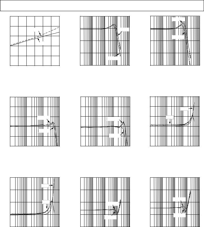
Typical Performance Characteristics–AD8350
|
50 |
|
|
|
|
|
|
mA |
40 |
|
|
|
|
|
|
|
|
|
VCC = 10V |
|
|
||
– |
|
|
|
|
|
|
|
CURRENT |
30 |
|
|
|
|
|
|
20 |
|
|
VCC = 5V |
|
|
||
SUPPLY |
|
|
|
|
|
|
|
10 |
|
|
|
|
|
|
|
|
|
|
|
|
|
|
|
|
0 |
–20 |
0 |
20 |
40 |
60 |
80 |
|
–40 |
||||||
|
|
|
TEMPERATURE – C |
|
|
||
TPC 1. Supply Current vs.
|
Temperature |
|
|
|
|
350 |
|
|
|
|
300 |
|
|
|
– |
250 |
|
VCC = 10V |
|
IMPEDANCE |
|
|
||
200 |
|
|
|
|
|
|
VCC = 5V |
|
|
|
|
|
|
|
|
150 |
|
|
|
|
100 |
|
|
|
|
1 |
10 |
100 |
1k |
FREQUENCY – MHz
TPC 4. AD8350-15 Input Impedance vs. Frequency
|
20 |
|
|
|
|
|
25 |
|
VCC = 10V |
|
|
|
|
|
|
|
|
|
|
|
|
||
|
15 |
|
|
VCC = 10V |
|
20 |
|
|
|
|
|
dB |
|
|
|
|
|
dB |
|
|
VCC = 5V |
|
|
– |
10 |
|
|
|
|
– |
15 |
|
|
|
|
GAIN |
|
|
|
|
GAIN |
|
|
|
|
||
|
|
|
|
|
|
|
|
|
|
||
|
5 |
|
|
|
|
|
10 |
|
|
|
|
|
|
|
|
VCC = 5V |
|
|
|
|
|
|
|
|
0 |
10 |
100 |
1k |
10k |
|
5 |
10 |
100 |
1k |
10k |
|
1 |
|
1 |
||||||||
|
|
|
FREQUENCY – MHz |
|
|
|
|
FREQUENCY – MHz |
|
||
TPC 2. AD8350-15 Gain (S21) vs. |
TPC 3. AD8350-20 Gain (S21) vs. |
||||||||||
Frequency |
|
|
|
Frequency |
|
|
|
||||
|
350 |
|
|
|
|
|
500 |
|
|
|
|
|
300 |
|
|
|
|
|
400 |
|
|
SOIC |
|
|
|
|
|
|
|
|
|
|
|
|
|
– |
250 |
|
|
|
|
– |
300 |
|
SOIC |
|
|
IMPEDANCE |
|
|
VCC = 10V |
|
IMPEDANCE |
|
|
|
|||
|
|
|
|
|
|
|
|
|
|||
|
|
|
|
|
|
|
|
|
|
|
|
|
200 |
|
|
|
|
|
200 |
|
|
|
|
|
150 |
|
|
VCC = 5V |
|
|
100 |
|
|
|
|
|
100 |
|
|
|
|
|
0 |
|
|
|
|
|
1 |
|
10 |
100 |
1k |
|
0 |
|
10 |
100 |
1000 |
FREQUENCY – MHz |
FREQUENCY – MHz |
TPC 5. AD8350-20 Input Impedance |
TPC 6. AD8350-15 Output Impedance |
vs. Frequency |
vs. Frequency |
|
800 |
|
|
|
|
|
|
SOIC |
|
|
600 |
|
|
|
– |
|
|
|
|
IMPEDANCE |
400 |
|
SOIC |
|
|
|
|
|
|
|
200 |
|
|
|
|
0 |
10 |
100 |
1000 |
|
0 |
|||
|
|
FREQUENCY – MHz |
|
|
TPC 7. AD8350-20 Output Impedance vs. Frequency
|
–5 |
|
|
|
|
|
–10 |
|
|
|
|
– dB |
|
|
|
|
|
ISOLATION |
–15 |
|
VCC = 10V |
|
|
|
|
|
|||
|
|
|
|
|
|
|
–20 |
|
VCC = 5V |
|
|
|
|
|
|
|
|
|
–25 |
10 |
100 |
1k |
10k |
|
1 |
||||
|
|
|
FREQUENCY – MHz |
|
|
TPC 8. AD8350-15 Isolation (S12) vs. Frequency
|
–10 |
|
|
|
|
|
–15 |
|
|
|
|
– dB |
|
|
VCC = 10V |
|
|
ISOLATION |
|
|
|
|
|
–20 |
|
|
|
|
|
|
|
|
|
|
|
|
–25 |
|
VCC = 5V |
|
|
|
–30 |
10 |
100 |
1k |
10k |
|
1 |
||||
|
|
|
FREQUENCY – MHz |
|
|
TPC 9. AD8350-20 Isolation (S12) vs. Frequency
REV. A |
–5– |
AD8350 |
|
|
|
|
|
||
|
–40 |
VOUT = 1V p-p |
|
|
|
|
|
|
|
|
|
|
|
||
|
–45 |
|
|
HD2 (VCC = 10V) |
|
||
– dBc |
–50 |
|
HD2 (VCC = 5V) |
|
|
||
–55 |
|
|
|
|
|
|
|
DISTORTION |
–60 |
|
|
|
HD3 (VCC = 5V) |
||
|
|
|
|
|
|
||
–65 |
|
|
|
HD3 (VCC = 10V) |
|
||
–70 |
|
|
|
|
|||
|
|
|
|
|
|
|
|
|
–75 |
|
|
|
|
|
|
|
–80 |
50 |
100 |
150 |
200 |
250 |
300 |
|
0 |
||||||
|
|
FUNDAMENTAL FREQUENCY – MHz |
|
||||
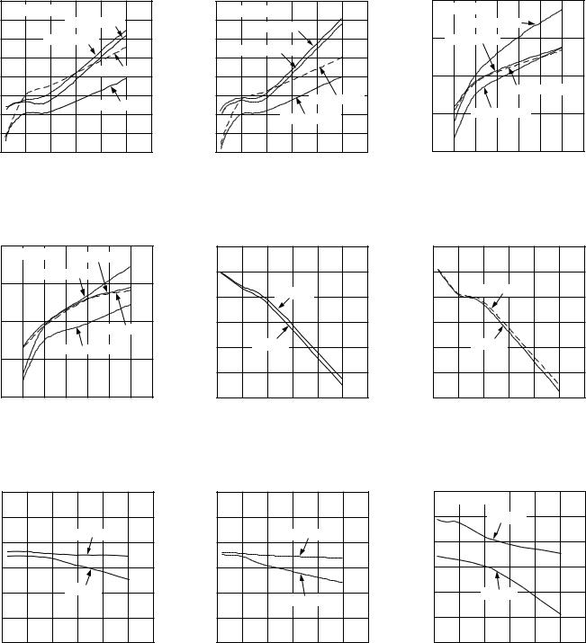
TPC 10. AD8350-15 Harmonic Distortion vs. Frequency
|
–45 |
FO = 50MHz |
|
|
|
|
|
|
|
|
|
HD2 (VCC = 5V) |
|
|
|||
|
|
|
|
|
|
|
||
|
|
|
HD3 (VCC = 5V) |
|
|
|
||
– dBc |
–55 |
|
|
|
|
|
|
|
|
|
|
|
|
|
|
|
|
DISTORTION |
–65 |
|
|
|
|
HD2 (VCC = 10V) |
||
|
|
|
|
|
||||
|
|
|
HD3 (VCC = 10V) |
|
|
|||
|
–75 |
|
|
|
|
|
|
|
|
–85 |
0.5 |
1 |
1.5 |
2 |
2.5 |
3 |
3.5 |
|
0 |
|||||||
|
|
|
OUTPUT VOLTAGE – V p-p |
|
|
|||
TPC 13. AD8350-20 Harmonic Distortion vs. Differential Output Voltage
|
41 |
|
|
|
|
|
|
|
36 |
|
|
|
|
|
|
) |
|
|
|
VCC = 10V |
|
|
|
50 |
31 |
|
|
|
|
|
|
(Re: |
26 |
|
|
|
|
|
|
– dBm |
|
|
|
|
|
|
|
|
|
|
VCC = 5V |
|
|
||
OIP3 |
21 |
|
|
|
|
||
|
|
|
|
|
|
|
|
|
16 |
|
|
|
|
|
|
|
11 |
50 |
100 |
150 |
200 |
250 |
300 |
|
0 |
||||||
|
|
|
FREQUENCY – MHz |
|
|
||
TPC 16. AD8350-15 Output Referred IP3 vs. Frequency
|
–40 |
VOUT = 1V p-p |
|
|
|
|
|
|
|
|
|
|
|
||
|
–45 |
|
HD2 (VCC = 5V) |
|
|
||
|
|
|
|
|
|||
– dBc |
–50 |
|
|
|
|
|
|
–55 |
HD2 (VCC = 10V) |
|
|
|
|||
|
|
|
|
|
|
||
DISTORTION |
–60 |
|
|
|
|
|
|
–65 |
|
|
|
HD3 (VCC = 5V) |
|||
–70 |
|
|
|
|
|
|
|
|
|
|
HD3 (VCC = 10V) |
|
|||
|
|
|
|
|
|||
|
–75 |
|
|
|
|
|
|
|
–80 |
50 |
100 |
150 |
200 |
250 |
300 |
|
0 |
||||||
|
|
FUNDAMENTAL FREQUENCY – MHz |
|
||||
TPC 11. AD8350-20 Harmonic Distortion vs. Frequency
|
66 |
|
|
|
|
|
|
|
61 |
|
|
|
|
|
|
50 ) |
56 |
|
|
VCC = 10V |
|
|
|
(Re: |
51 |
|
|
|
|
|
|
– dBm |
|
|
|
|
|
|
|
|
|
VCC = 5V |
|
|
|
||
OIP2 |
46 |
|
|
|
|
||
|
|
|
|
|
|
|
|
|
41 |
|
|
|
|
|
|
|
36 |
50 |
100 |
150 |
200 |
250 |
300 |
|
0 |
||||||
|
|
|
FREQUENCY – MHz |
|
|
||
TPC 14. AD8350-15 Output Referred IP2 vs. Frequency
|
41 |
|
|
|
|
|
|
|
36 |
|
|
|
|
|
|
) |
|
|
|
VCC = 10V |
|
|
|
50 |
31 |
|
|
|
|
|
|
(Re: |
26 |
|
|
|
|
|
|
– dBm |
|
|
|
|
|
|
|
|
|
|
|
|
|
|
|
OIP3 |
21 |
|
|
VCC = 5V |
|
|
|
|
|
|
|
|
|||
|
16 |
|
|
|
|
|
|
|
11 |
50 |
100 |
150 |
200 |
250 |
300 |
|
0 |
||||||
|
|
|
FREQUENCY – MHz |
|
|
||
TPC 17. AD8350-20 Output Referred IP3 vs. Frequency
|
–45 |
FO = 50MHz |
|
|
|
|
|
|
|
|
|
|
|
|
|
||
|
|
|
HD3 (VCC = 5V) |
|
|
|
||
– dBc |
–55 |
HD2 (VCC = 5V) |
|
|
|
|
||
|
|
|
|
|
|
|
|
|
DISTORTION |
–65 |
|
|
|
|
|
|
|
|
|
|
|
HD2 (VCC = 10V) |
|
|||
–75 |
|
HD3 (VCC = 10V) |
|
|
|
|||
|
|
|
|
|
||||
|
–85 |
0.5 |
1 |
1.5 |
2 |
2.5 |
3 |
3.5 |
|
0 |
|||||||
|
|
|
OUTPUT VOLTAGE – V p-p |
|
|
|||
TPC 12. AD8350-15 Harmonic Distortion vs. Differential Output Voltage
|
66 |
|
|
|
|
|
|
|
61 |
|
|
|
|
|
|
) |
|
|
VCC = 10V |
|
|
|
|
50 |
56 |
|
|
|
|
|
|
(Re: |
51 |
|
|
|
|
|
|
– dBm |
|
|
|
|
|
|
|
|
|
VCC = 5V |
|
|
|
||
OIP2 |
46 |
|
|
|
|
||
|
|
|
|
|
|
|
|
|
41 |
|
|
|
|
|
|
|
36 |
50 |
100 |
150 |
200 |
250 |
300 |
|
0 |
||||||
|
|
|
FREQUENCY – MHz |
|
|
||
TPC 15. AD8350-20 Output Referred IP2 vs. Frequency
10.0 
 INPUT REFERRED
50 ) |
7.5 |
|
VCC = 10V |
|
|
|
|
(Re: |
|
|
|
|
|
|
|
– dBm |
5.0 |
|
|
|
|
|
|
|
|
|
|
|
|
|
|
COMPRESSION |
2.5 |
|
|
|
|
|
|
0 |
|
VCC = 5V |
|
|
|
||
–2.5 |
|
|
|
|
|
|
|
1dB |
|
|
|
|
|
|
|
|
|
|
|
|
|
|
|
|
–5.0 0 |
100 |
200 |
300 |
400 |
500 |
600 |
|
|
|
FREQUENCY – MHz |
|
|
||
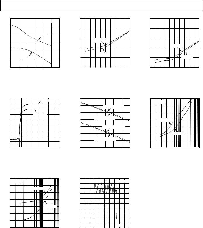
TPC 18. AD8350-15 1 dB Compression vs. Frequency
–6– |
REV. A |
|
|
|
|
|
|
|
|
|
|
|
|
|
AD8350 |
|
7.5 |
|
|
|
INPUT REFERRED |
10 |
|
|
10 |
|
|
||
50 ) |
|
|
|
|
|
|
|
|
|
|
|||
5.0 |
|
|
|
|
|
|
9 |
|
|
9 |
|
|
|
COMPRESSION– dBm (Re: |
|
|
|
|
|
|
|
|
|
|
|||
|
|
|
|
|
|
|
|
|
|
|
|||
2.5 |
|
|
VCC = 10V |
|
|
|
|
|
|
|
|
||
|
|
|
|
|
|
|
8 |
|
|
8 |
|
VCC = 5V |
|
0 |
|
|
|
|
|
|
dBFIGURENOISE– |
|
VCC = 10V |
dBFIGURENOISE– |
|
||
|
|
|
|
|
|
|
|
|
|
|
|
||
|
|
|
|
|
|
|
|
|
|
|
|
|
|
|
|
|
|
|
|
|
|
7 |
|
|
7 |
|
VCC = 10V |
|
|
|
|
|
|
|
|
|
|
|
|
||
|
–2.5 |
|
|
|
|
|
|
|
|
|
|
|
|
|
|
|
|
|
|
|
|
|
|
VCC = 5V |
|
|
|
1dB |
–5.0 |
|
VCC = 5V |
|
|
|
|
6 |
|
|
6 |
|
|
|
|
|
|
|
|
|
|
|
|
|
|
|
|
|
–7.5 |
|
|
|
|
|
|
5 |
|
|
5 |
|
|
|
0 |
100 |
200 |
300 |
400 |
500 |
600 |
0 |
50 |
100 150 200 250 300 350 400 450 500 |
0 |
50 |
100 150 200 250 300 350 400 450 500 |
|
|
|
FREQUENCY – MHz |
|
|
|
|
FREQUENCY – MHz |
|
|
FREQUENCY – MHz |
||
TPC 19. AD8350-20 1 dB Compres- |
TPC 20. AD8350-15 Noise Figure |
TPC 21. AD8350-20 Noise Figure |
sion vs. Frequency |
vs. Frequency |
vs. Frequency |
|
25 |
|
|
|
|
|
AD8350-20 |
|
||
|
|
|
|
|
|
|
|
|||
|
20 |
|
|
|
|
|
|
|
|
|
|
15 |
|
|
|
|
|
|
|
|
|
|
10 |
|
|
|
|
AD8350-15 |
|
|
|
|
dB |
5 |
|
|
|
|
|
|
|
|
|
– |
|
|
|
|
|
|
|
|
|
|
GAIN |
0 |
|
|
|
|
|
|
|
|
|
|
|
|
|
|
|
|
|
|
|
|
|
–5 |
|
|
|
|
|
|
|
|
|
|
–10 |
|
|
|
|
|
|
|
|
|
|
–15 |
|
|
|
|
|
|
|
|
|
|
–20 |
2 |
3 |
4 |
5 |
6 |
7 |
8 |
9 |
10 |
|
1 |
|||||||||
|
|
|
|
|
VCC – Volts |
|
|
|
|
|
TPC 22. AD8350 Gain (S21) vs. Supply Voltage
|
–20 |
VCC = 5V |
|
|
|
|
|
|
|
|
–30 |
|
AD8350-20 |
|
|
|
|
|
|
|
–40 |
|
|
|
dB |
–50 |
|
|
|
– |
|
|
|
|
|
|
|
|
|
PSRR |
–60 |
|
AD8350-15 |
|
|
|
|
|
|
|
–70 |
|
|
|
|
–80 |
|
|
|
|
–90 |
|
|
|
|
1 |
10 |
100 |
1k |
|
|
FREQUENCY – MHz |
|
|
|
100 |
|
|
|
|
|
|
|
50 |
|
|
VOUT + (VCC = 5V) |
|
||
|
|
|
|
|
|||
mV |
0 |
|
|
|
|
|
|
– |
|
|
|
|
|
|
|
OFFSET |
–50 |
|
VOUT – (VCC = 5V) |
|
|
||
|
|
|
|
|
|
||
–100 |
|
|
|
|
|
|
|
OUTPUT |
|
|
VOUT + (VCC = 10V) |
|
|||
–150 |
|
|
|
|
|
|
|
|
|
|
|
|
|
|
|
|
–200 |
|
VOUT – (VCC = 10V) |
|
|
||
|
|
|
|
|
|
|
|
|
–250 |
–20 |
0 |
20 |
40 |
60 |
80 |
|
–40 |
||||||
|
|
|
TEMPERATURE – C |
|
|
||
TPC 23. AD8350 Output Offset Voltage vs. Temperature
500mV |
VCC = |
5V |
VOUT |
|
|
ENBL |
|
|
5V |
30ns |
|
|
–20 |
|
|
|
|
|
VCC = 5V |
|
|
|
–30 |
|
|
|
|
–40 |
|
|
|
dB |
–50 |
AD8350-20 |
|
|
– |
|
|
||
|
|
|
|
|
PSRR |
–60 |
|
|
|
|
|
|
|
|
|
–70 |
|
AD8350-15 |
|
|
–80 |
|
|
|
|
–90 |
|
|
|
|
1 |
10 |
100 |
1k |
|
|
FREQUENCY – MHz |
|
|
TPC 24. AD8350 PSRR vs. Frequency
TPC 25. AD8350 CMRR vs. Frequency |
TPC 26. AD8350 Power-Up/Down |
|
Response Time |
REV. A |
–7– |
AD8350
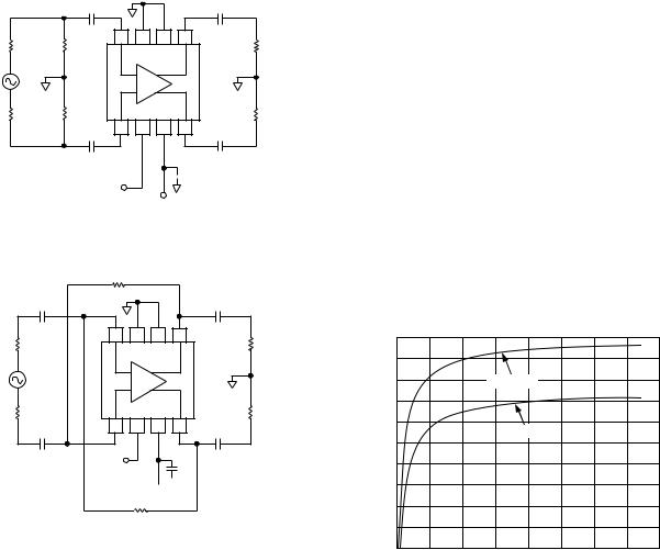
APPLICATIONS
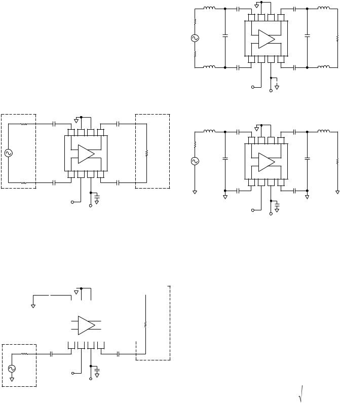
Using the AD8350
Figure 1 shows the basic connections for operating the AD8350. A single supply in the range 5 V to 10 V is required. The power supply pin should be decoupled using a 0.1 µF capacitor. The ENBL pin is tied to the positive supply or to 5 V (when VCC = 10 V) for normal operation and should be pulled to ground to put the device in sleep mode. Both the inputs and the outputs have dc bias levels at midsupply and should be ac-coupled.
Also shown in Figure 1 are the impedance balancing requirements, either resistive or reactive, of the input and output. With an input and output impedance of 200 Ω, the AD8350 should be driven by a 200 Ω source and loaded by a 200 Ω impedance. A reactive match can also be implemented.
|
C2 |
|
|
|
C4 |
|
SOURCE |
0.001 F |
|
|
|
0.001 F |
LOAD |
Z = 100 |
8 |
7 |
6 |
5 |
|
|
|
|
|
||||
|
|
AD8350 |
|
|
|
|
|
|
– |
|
|
|
Z = 200 |
|
|
|
|
|
|
|
|
|
+ |
|
|
|
|
Z = 100 |
1 |
2 |
3 |
4 |
|
|
|
|
|
|
|
|
|
|
C1 |
|
|
|
C3 |
|
|
0.001 F |
|
|
C5 |
0.001 F |
|
|
|
|
|
|
|
|
0.1 F
ENBL (5V)
LS/2 |
CAC |
|
|
CAC |
|
LS/2 |
RS/2 |
8 |
7 |
6 |
5 |
|
|
|
AD8350 |
|
|
|
||
|
|
|
|
|
||
CP |
|
– |
|
|
CP |
RLOAD |
VS |
|
+ |
|
|
|
|
RS/2 |
1 |
2 |
3 |
4 |
|
|
|
|
|
||||
LS/2 |
CAC |
|
|
CAC |
|
LS/2 |
 0.1 F
0.1 F
ENBL (5V)
+VS (5V TO 10V)
Figure 3. Reactively Matching the Input and Output
LS |
CAC |
|
|
CAC |
|
LS |
RS |
8 |
7 |
6 |
5 |
|
|
|
AD8350 |
|
|
|
||
|
|
|
|
|
||
VS |
CP |
– |
|
|
CP |
RLOAD |
|
+ |
|
|
|
||
|
1 |
2 |
3 |
4 |
|
|
|
CAC |
|
|
CAC |
|
|
|
|
|
|
0.1 F |
|
|
+VS (5V TO 10V) |
ENBL (5V) |
Figure 1. Basic Connections for Differential Drive
Figure 2 shows how the AD8350 can be driven by a singleended source. The unused input should be ac-coupled to ground. When driven single-endedly, there will be a slight imbalance in the differential output voltages. This will cause an increase in the second order harmonic distortion (at 50 MHz, with VCC =
10 V and VOUT = 1 V p-p, –59 dBc was measured for the second harmonic on AD8350-15).
|
|
|
|
|
|
|
|
|
|
|
|
|
|
|
|
|
|
|
|
|
|
|
|
|
|
|
|
|
|
|
|
|
|
|
|
|
|
|
|
|
|
|
|
|
|
|
|
|
|
|
|
|
|
|
|
|
|
|
|
|
|
|
|
|
|
LOAD |
|||||||
|
|
|
|
|
|
|
|
|
|
|
|
|
|
|
|
|
|
|
|
|
|
|
|
|
|
|
|
|
||||||||
C2 |
|
|
|
|
|
|
|
|
|
|
|
C4 |
|
|
|
|
|
|
|
|
|
|
|
|
|
|
|
|||||||||
0.001 F |
8 |
|
|
7 |
|
6 |
|
5 |
|
0.001 F |
|
|
|
|
|
|
|
|
|
|
|
|
|
|
|
|||||||||||
|
|
|
|
|
|
|
|
AD8350 |
|
|
|
|
|
|
|
|
|
|
|
|
|
|
|
|
|
|
|
|
|
|
|
|||||
|
|
|
|
|
|
|
|
|
|
|
|
|
|
|
|
|
|
|
|
|
|
|
|
|
|
|
|
|
|
|
||||||
|
|
|
|
|
|
|
|
|
|
|
|
|
|
|
|
|
|
|
|
|
|
|
|
|
|
|
|
|
|
|
||||||
|
|
|
|
|
|
|
|
|
|
– |
|
|
|
|
|
|
|
|
|
|
|
|
|
|
|
|
|
Z = 200 |
||||||||
|
|
|
|
|
|
|
|
|
|
|
|
|
|
|
|
|
|
|
|
|
|
|
|
|
|
|
||||||||||
|
|
|
|
|
|
|
|
|
|
|
|
|
|
|
|
|
|
|
|
|
|
|
|
|
|
|
||||||||||
|
|
|
|
|
|
|
|
+ |
|
|
|
|
|
|
|
|
|
|
|
|
|
|
|
|
|
|||||||||||
|
|
|
|
|
|
|
|
|
|
|
|
|
|
|
|
|
|
|
|
|
|
|
|
|
|
|
|
|
|
|
|
|
|
|||
|
|
|
|
|
|
|
|
|
|
|
|
|
|
|
|
|
|
|
|
|
|
|
|
|
|
|
|
|
|
|
|
|
|
|
|
|
|
|
|
|
|
|
|
|
|
|
|
|
|
|
|
|
|
|
|
|
|
|
|
|
|
|
|
|
|
|
|
|
|
|
|
|
|
|
|
|
|
|
|
|
|
|
|
|
|
|
|
|
|
|
|
|
|
|
|
|
|
|
|
|
|
|
|
|
|
|
|
|
|
|
|
|
|
|
|
|
|
|
|
|
|
|
|
|
|
|
|
|
|
|
|
|
|
|
|
|
|
|
|
|
|
|
|
|
|
|
|
1 2 3 4
SOURCE
Z = 200 |
C1 |
C3 |
|
0.001 F |
0.001 F |
|
|
C5 |
|
ENBL (5V) |
0.1 F |
+VS (5V TO 10V)
Figure 2. Basic Connections for Single-Ended Drive
Reactive Matching
In practical applications, the AD8350 will most likely be matched using reactive matching components as shown in Figure 3. Matching components can be calculated using a Smith Chart or by using a resonant approach to determine the matching network that results in a complex conjugate match. In either situation, the circuit can be analyzed as a single-ended equivalent circuit to ease calculations as shown in Figure 4.
+VS (5V TO 10V)
Figure 4. Single-Ended Equivalent Circuit
When the source impedance is smaller than the load impedance, a step-up matching network is required. A typical step-up network is shown on the input of the AD8350 in Figure 3. For purely resistive source and load impedances the resonant approach may be used. The input and output impedance of the AD8350 can be modeled as a real 200 Ω resistance for operating frequencies less than 100 MHz. For signal frequencies exceeding 100 MHz, classical Smith Chart matching techniques should be invoked in order to deal with the complex impedance relationships. Detailed S parameter data measured differentially in a 200 Ω system can be found in Tables II and III.
For the input matching network the source resistance is less than the input resistance of the AD8350. The AD8350 has a nominal 200 Ω input resistance from Pins 1 to 8. The reactance of the ac-coupling capacitors, CAC, should be negligible if 100 nF capacitors are used and the lowest signal frequency is greater than 1 MHz. If the series reactance of the matching network inductor is defined to be XS = 2 π f LS, and the shunt reactance of the matching capacitor to be XP = (2 π f CP)–1, then:
X |
S |
= |
RS × RLOAD |
where X |
P |
= R |
× |
RS |
(1) |
|
|
||||||||
|
|
XP |
LOAD |
|
RLOAD – RS |
||||
|
|
|
|
|
|
|
|||
For a 70 MHz application with a 50 Ω source resistance, and
assuming the input impedance is 200 Ω, or RLOAD = RIN = 200 Ω, then XP = 115.5 Ω and XS = 86.6 Ω, which results in the follow-
ing component values:
CP = (2 |
π × 70 × 106 × 115.5)–1 = 19.7 pF and |
LS = |
86.6 × (2 π × 70 × 106)–1 = 197 nH |
–8– |
REV. A |

AD8350
For the output matching network, if the output source resistance of the AD8350 is greater than the terminating load resistance, a step-down network should be employed as shown on the output of Figure 3. For a step-down matching network, the series and parallel reactances are calculated as:
XS = |
RS × RLOAD |
where XP = RS × |
RLOAD |
(2) |
|
RS – RLOAD |
|||
|
XP |
|
||
For a 10 MHz application with the 200 Ω output source resistance
of the AD8350, RS = 200 Ω, and a 50 Ω load termination, RLOAD = 50 Ω, then XP = 115.5 Ω and XS = 86.6 Ω, which results in
the following component values:
CP = (2 π × 10 × 106 × 115.5)–1 = 138 pF and
LS = 86.6 × (2 π × 10 × 106)–1 = 1.38 µH
The same results can be obtained using the plots in Figure 5 and Figure 6. Figure 5 shows the normalized shunt reactance versus the normalized source resistance for a step-up matching network, RS < RLOAD. By inspection, the appropriate reactance
can be found for a given value of RS/RLOAD. The series reactance is then calculated using XS = RS RLOAD/XP. The same technique can be used to design the step-down matching network using
Figure 6.
|
2 |
|
|
|
|
|
|
|
|
|
|
|
|
|
|
|
|
|
|
|
LOAD |
1.8 |
|
|
RSOURCE |
|
XS |
|
|
|
|
|
|
|
|
|
|
|
|
||
1.6 |
|
|
|
|
|
|
|
|
|
|
|
|
|
|
|
|
|
|
||
/R |
|
|
|
|
|
|
|
XP |
|
R |
|
|
|
|
|
|
|
|
||
|
|
|
|
|
|
|
|
|
|
|
|
|
|
|
|
|
||||
P |
|
|
|
|
|
|
|
|
|
LOAD |
|
|
|
|
|
|
|
|||
– X |
1.4 |
|
|
|
|
|
|
|
|
|
|
|
|
|
|
|
|
|
|
|
REACTANCE |
1.2 |
|
|
|
|
|
|
|
|
|
|
|
|
|
|
|
|
|
|
|
1 |
|
|
|
|
|
|
|
|
|
|
|
|
|
|
|
|
|
|
|
|
0.8 |
|
|
|
|
|
|
|
|
|
|
|
|
|
|
|
|
|
|
|
|
NORMALIZED |
|
|
|
|
|
|
|
|
|
|
|
|
|
|
|
|
|
|
|
|
0.6 |
|
|
|
|
|
|
|
|
|
|
|
|
|
|
|
|
|
|
|
|
0.4 |
|
|
|
|
|
|
|
|
|
|
|
|
|
|
|
|
|
|
|
|
0.2 |
|
|
|
|
|
|
|
|
|
|
|
|
|
|
|
|
|
|
|
|
|
|
|
|
|
|
|
|
|
|
|
|
|
|
|
|
|
|
|
|
|
|
0 |
|
|
|
|
|
|
|
|
|
|
|
|
|
|
|
|
|
|
|
|
0.01 |
0.05 |
0.09 |
0.13 |
0.17 |
0.21 |
0.25 |
0.29 |
0.33 |
0.37 |
0.41 |
0.45 |
0.49 |
0.53 |
0.57 |
0.61 |
0.65 |
0.69 |
0.73 |
0.77 |
|
|
NORMALIZED SOURCE RESISTANCE – RSOURCE/R LOAD |
|
|||||||||||||||||
Figure 5. Normalized Step-Up Matching Components
|
3.2 |
|
|
|
|
|
|
|
|
|
|
|
|
|
|
|
|
|
LOAD |
|
|
RSOURCE |
|
|
XS |
|
|
|
|
|
|
|
|
|
|
||
3 |
|
|
|
|
|
|
|
|
|
|
|
|
|
|
|
|
||
|
|
|
|
XP |
|
|
RLOAD |
|
|
|
|
|
|
|
||||
|
|
|
|
|
|
|
|
|
|
|
|
|
|
|||||
/R |
|
|
|
|
|
|
|
|
|
|
|
|
|
|
|
|
|
|
P |
|
|
|
|
|
|
|
|
|
|
|
|
|
|
|
|
|
|
– X |
2.8 |
|
|
|
|
|
|
|
|
|
|
|
|
|
|
|
|
|
REACTANCE |
|
|
|
|
|
|
|
|
|
|
|
|
|
|
|
|
|
|
2.6 |
|
|
|
|
|
|
|
|
|
|
|
|
|
|
|
|
|
|
|
|
|
|
|
|
|
|
|
|
|
|
|
|
|
|
|
|
|
NORMALIZED |
2.4 |
|
|
|
|
|
|
|
|
|
|
|
|
|
|
|
|
|
2.2 |
|
|
|
|
|
|
|
|
|
|
|
|
|
|
|
|
|
|
|
|
|
|
|
|
|
|
|
|
|
|
|
|
|
|
|
|
|
|
2 |
|
|
|
|
|
|
|
|
|
|
|
|
|
|
|
|
|
|
2 |
2.4 |
2.8 |
3.2 |
3.6 |
4 |
4.4 |
4.8 |
5.2 |
5.6 |
6 |
6.4 |
6.8 |
7.2 |
7.6 |
8 |
8.4 |
8.8 |
|
|
NORMALIZED SOURCE RESISTANCE – RSOURCE/R LOAD |
|
|||||||||||||||
Figure 6. Normalized Step-Down Matching Components
The same results could be found using a Smith Chart as shown in Figure 7. In this example, a shunt capacitor and a series inductor are used to match the 200 Ω source to a 50 Ω load. For a frequency of 10 MHz, the same capacitor and inductor values previously found using the resonant approach will transform the 200 Ω source to match the 50 Ω load. At frequencies exceeding 100 MHz, the S parameters from Tables II and III should be used to account for the complex impedance relationships.
LOAD |
SOURCE |
SHUNT C
SERIES L
Figure 7. Smith Chart Representation of Step-Down Network
After determining the matching network for the single-ended equivalent circuit, the matching elements need to be applied in a differential manner. The series reactance needs to be split such that the final network is balanced. In the previous examples, this simply translates to splitting the series inductor into two equal halves as shown in Figure 3.
Gain Adjustment
The effective gain of the AD8350 can be reduced using a number of techniques. Obviously a matched attenuator network will reduce the effective gain, but this requires the addition of a separate component which can be prohibitive in size and cost. The attenuator will also increase the effective noise figure resulting in an SNR degradation. A simple voltage divider can be implemented using the combination of the driving impedance of the previous stage and a shunt resistor across the inputs of the AD8350 as shown in Figure 8. This provides a compact solution but suffers from an increased noise spectral density at the input of the AD8350 due to the thermal noise contribution of the shunt resistor. The input impedance can be dynamically altered through the use of feedback resistors as shown in Figure 9. This will result in a similar attenuation of the input signal by virtue of the voltage divider established from the driving source impedance and the reduced input impedance of the AD8350. Yet this technique does not significantly degrade the SNR with the unnecessary increase in thermal noise that arises from a truly resistive attenuator network.
REV. A |
–9– |
AD8350
CAC |
CAC |
RS |
8 |
7 |
6 |
5 |
RL |
R |
|
|
|
||
|
SHUNT |
AD8350 |
|
|
|
|
|
|
|
||
VS |
|
– |
|
|
|
|
|
|
|
|
|
|
|
+ |
|
|
|
RS |
RSHUNT |
|
|
|
RL |
|
1 |
2 |
3 |
4 |
|
|
CAC |
|
|
|
CAC |
 0.1 F
0.1 F
ENBL (5V)
+VS (5V TO 10V)
Figure 8. Gain Reduction Using Shunt Resistor
|
RFEXT |
|
|
|
|
CAC |
|
|
|
|
CAC |
RS |
8 |
7 |
6 |
5 |
RL |
|
AD8350 |
||||
|
|
|
|||
VS |
|
– |
|
|
|
|
|
|
|
|
|
|
|
+ |
|
|
|
RS |
|
|
|
|
RL |
|
1 |
2 |
3 |
4 |
|
CAC |
ENBL |
|
|
0.1 F |
CAC |
|
|
|
|||
|
(5V) |
|
|
|
|
+VS 
 (5V TO 10V)
RFEXT
Figure 9. Dynamic Gain Reduction
Figure 8 shows a typical implementation of the shunt divider concept. The reduced input impedance that results from the parallel combination of the shunt resistor and the input impedance of the AD8350 adds attenuation to the input signal effectively reducing the gain. For frequencies less than 100 MHz, the input impedance of the AD8350 can be modeled as a real 200 Ω resistance (differential). Assuming the frequency is low enough to ignore the shunt reactance of the input, and high enough such that the reactance of moderately sized ac-coupling capacitors can be considered negligible, the insertion loss, IL, due to the shunt divider can be expressed as:
|
|
|
|
RIN |
|
|
|
||
|
|
|
|
|
|
|
|
|
|
|
|
|
(RIN + RS ) |
||||||
IL(dB) = 20 |
Log10 |
|
|
|
|
|
|
||
|
RIN RSHUNT |
|
|
||||||
|
|
|
|
|
|
||||
|
|
|
|
|
|
|
|
|
|
|
|
|
|
|
|
||||
|
|
(RIN RSHUNT + |
RS ) |
||||||
where |
(3) |
||
RIN RSHUNT = |
RIN RSHUNT |
and RIN = 100Ω single−ended |
|
RIN + RSHUNT |
|||
|
|
||
The insertion loss and the resultant power gain for multiple shunt resistor values is summarized in Table I. The source resistance and input impedance need careful attention when using Equation 1. The reactance of the input impedance of the AD8350 and the ac-coupling capacitors need to be considered before assuming they have negligible contribution. Figure 10
shows the effective power gain for multiple values of RSHUNT for the AD8350-15 and AD8350-20.
Table I. Gain Adjustment Using Shunt Resistor, RS = 100 and RIN = 100 Single-Ended
|
|
Power Gain–dB |
||
RSHUNT– |
IL–dB |
AD8350-15 |
|
AD8350-20 |
|
||||
50 |
6.02 |
8.98 |
|
13.98 |
100 |
3.52 |
11.48 |
|
16.48 |
200 |
1.94 |
13.06 |
|
18.06 |
300 |
1.34 |
13.66 |
|
18.66 |
400 |
1.02 |
13.98 |
|
18.98 |
|
|
|
|
|
|
20 |
|
|
|
|
|
|
|
|
|
18 |
|
|
|
|
|
|
|
|
|
16 |
|
|
AD8350-20 |
|
|
|
|
|
|
14 |
|
|
|
|
|
|
|
|
dB |
12 |
|
|
AD8350-15 |
|
|
|
|
|
|
|
|
|
|
|
|
|||
– |
|
|
|
|
|
|
|
||
10 |
|
|
|
|
|
|
|
|
|
GAIN |
|
|
|
|
|
|
|
|
|
8 |
|
|
|
|
|
|
|
|
|
|
|
|
|
|
|
|
|
|
|
|
6 |
|
|
|
|
|
|
|
|
|
4 |
|
|
|
|
|
|
|
|
|
2 |
|
|
|
|
|
|
|
|
|
0 |
100 |
200 |
300 |
400 |
500 |
600 |
700 |
800 |
|
0 |
||||||||
|
|
|
|
|
RSHUNT – |
|
|
|
|
Figure 10. Gain for Multiple Values of Shunt Resistance for Circuit in Figure 8
The gain can be adjusted dynamically by employing external feedback resistors as shown in Figure 9. The effective attenuation is a result of the lowered input impedance as with the shunt resistor method, yet there is no additional noise contribution at the input of the device. It is necessary to use well-matched resistors to minimize common-mode offset errors. Quality 1% tolerance resistors should be used along with a symmetric board layout to help guarantee balanced performance. The effective gain for multiple values of external feedback resistors is shown in Figure 11.
–10– |
REV. A |